

I. INTRODUCTION
When grain size is reduced below 100 nm, grain boundaries begin to account for a significant volume fraction of a material, and grain boundary processes start to control the plasticity of these nanocrystalline materials. Traditional intragranular dislocation mechanisms are suppressed and interfacial mechanisms such as grain boundary dislocation emission,Reference Asaro, Krysl and Kad1–Reference Cheng, Spencer and Milligan3 grain boundary migration,Reference Gianola, Van Petegem, Legros, Brandstetter, Van Swygenhoven and Hemker4–Reference Rupert, Gianola, Gan and Hemker7 grain boundary shear accommodated rotation,Reference Ke, Hackney, Milligan and Aifantis8–Reference Shan, Stach, Wiezorek, Knapp, Follstaedt and Mao10 and grain boundary slidingReference Schiotz, Di Tolla and Jacobsen11, Reference Van Swygenhoven and Derlet12 become the dominant deformation mechanisms. The common feature of these new mechanisms is the emphasis placed on the boundaries, which no longer only act as barriers to slip transmission but also become the primary facilitators for plastic deformation.
Because of the elevated importance of grain boundaries in nanocrystalline materials, increased attention has been focused on studying the atomic structure of boundaries in these materials. A number of studies have reported that, in their as-deposited or as-prepared state, nanocrystalline metals often contain nonequilibrium grain boundaries with excess dislocations, misfit regions, or excess free volume.Reference Jang and Atzmon13–Reference Wu and Zhu15 It has also been shown that these nonequilibrium boundaries evolve during thermal annealing, where kinetic processes can work to annihilate excess defects through a process termed “grain boundary relaxation,” which is a low-temperature process that can occur without any measurable change in grain size or texture. Grain boundary relaxation upon annealing has been observed through high-resolution transmission electron microscopy (TEM) of nanocrystalline Fe prepared by high-energy ball milling,Reference Jang and Atzmon13 where initially disconnected lattice planes commonly seen in the as-prepared material apparently evolved into more equilibrated structures with regularly spaced grain boundary dislocations upon annealing. X-ray atomic distribution function analysis of nanocrystalline PdReference Loffler and Weissmuller16 has suggested that grain boundary regions became more ordered after thermal exposure. Calorimetry experiments have also provided evidence for grain boundary relaxation through the observation of exothermic signals prior to the onset of grain growth.Reference Eckert, Holzer, Krill and Johnson17–Reference Tschope, Birringer and Gleiter19 Detor and SchuhReference Detor and Schuh20 showed that this heat release scales directly with grain boundary area, supporting the interpretation that such an exothermic peak is associated with a grain boundary relaxation process.
Since grain boundaries are central to plasticity in nanocrystalline materials and since excess boundary defects could facilitate plasticity by acting as additional sources and sinks for dislocations or as facilitators of grain boundary sliding, the relaxation of nonequilibrium boundaries should greatly impact mechanical properties in nanocrystalline materials. In fact, recent experiments have connected the relaxation of grain boundary structure to a pronounced strengthening effect in annealed nanocrystalline materials and also suggest that heat-treated nanocrystalline alloys have a different dependence of strength on grain size.Reference Chang, Kao and Chen21–Reference Fougere, Weertman, Siegel and Kim24 Further isolating this effect, careful experiments have shown that low-temperature annealing treatments can significantly increase hardnessReference Detor and Schuh20, Reference Wang, Cheng, Wei, Ma, Nieh and Hamza25 and tensile yield strength,Reference Wang, Cheng, Wei, Ma, Nieh and Hamza25 while grain size remains constant. Molecular dynamics (MD) simulations of relaxation strengthening have shown that annealing lowers the number of atoms that are considered to be part of the boundary (increases atomic registry at the boundaries) and shifts the energy of the grain boundary atoms to lower values.Reference Hasnaoui, Van Swygenhoven and Derlet26–Reference Vo, Averback, Bellon and Caro28 All of these studies point to the fact that grain size is not the only structural parameter of interest for nanocrystalline materials; grain boundary state can also dramatically alter mechanical properties and should be considered when attempting to improve material performance.
In spite of the above progress, to date, very little is known about the time and temperature dependence of grain boundary relaxation strengthening, any physical limits on it, or how it affects the mechanisms of deformation at the finest grain sizes. In addition, most previous studies have focused on annealing from a single isolated grain size, making it difficult to observe trends without comparing across different studies and materials. The purpose of this article is to provide a more methodical study of some of these open questions related to grain boundary relaxation strengthening in one technologically relevant family of nanocrystalline alloys. We begin by reporting on the kinetics of strengthening at two critical nanocrystalline grain sizes using controlled annealing treatments at multiple temperatures. Next, the effect of relaxation on the strength and dominant deformation mechanisms of alloys with grain sizes from 3 to 100 nm is explored. Drawing insight from these experiments, we discuss possible mechanisms for grain boundary relaxation and the resultant hardening effects.
II. EXPERIMENTAL METHODS
Nanocrystalline Ni–W specimens of 50- to 100-μm thickness were produced by pulsed electrodeposition, using the bath chemistry and deposition conditions of Detor and Schuh.Reference Detor and Schuh20, Reference Detor and Schuh29 Commercial purity Ni substrates were used as the cathodes for the deposition process, with a platinum mesh as the anode. Before deposition, the Ni cathodes were mechanically polished and electrocleaned. Following Detor and Schuh, the applied current waveform was systematically adjusted to produce alloys with different average grain sizes (d). The composition and grain size of these alloys are intimately connected, with increased W content promoting finer grain sizes.Reference Detor and Schuh29 Although composition changes with grain size, previous research has shown that the grain boundary excess of W is relatively constant for the entire range of grain sizes to be studied here (boundary excesses of ∼4–8 at.% W).Reference Detor, Miller and Schuh30, Reference Detor, Miller and Schuh31 Perhaps more importantly, microstructural evolution studies of nanocrystalline Ni–WReference Detor and Schuh20 have shown that grain boundary relaxation always precedes other types of structural evolution (grain growth, precipitation of second phases, and short-range chemical ordering), making Ni–W an ideal candidate for isolating the effects of nonequilibrium grain boundary structure. Prior work has isolated solid solution-strengthening effects in these materials,Reference Rupert, Trenkle and Schuh32 showing that W addition increases strength but does not alter the dominant deformation physics. After deposition, specimens were isothermally annealed at temperatures from 150 to 300 °C, followed by a water quench. These annealing temperatures are relatively mild for the Ni–W system and were chosen to avoid grain growth and chemical ordering, following an earlier study of the thermal stability of Ni–W.Reference Detor and Schuh20 Each specimen was mechanically polished to a root-mean-square roughness of <10 nm to give a surface suitable for indentation testing.
Structural characterization of both as-deposited and annealed specimens was performed by x-ray diffraction (XRD) using a Rigaku RU300 diffractometer (Tokyo, Japan) with a rotating Cu Kα radiation source operated at 50 kV and 300 mA. The XRD profiles were used to confirm that the alloys were polycrystalline face-centered cubic solid solutions and to estimate the average grain size to within ±25% by applying the integral breadth methodReference Zhang, Zhou and Lavernia33 to the {111} family of peaks after subtracting instrumental broadening. For the smallest grain sizes, only the (111) peak was available and the single peak Scherrer analysisReference Cullity34 was used. These analysis techniques have been shown to be accurate for Ni–W alloys in Refs. Reference Detor and Schuh20, Reference Detor and Schuh29, and Reference Trelewicz and Schuh35, where the measured XRD grain sizes were confirmed by TEM. TEM observations in this study were performed with a JEOL 2010 (Tokyo, Japan) operated at 200 kV in bright-field imaging mode. TEM specimens were prepared using a Fischione 1010 Ion Mill (Export, PA), with liquid nitrogen cooling to prevent structural evolution during milling. Scanning electron microscopy (SEM) with a FEI/Philips FEG ESEM (Hillsboro, OR) operating at 10 kV in high vacuum mode was used to investigate the surface morphology of selected residual impressions from nanoindentation.
Mechanical properties were measured with either Vickers microhardness or instrumented nanoindentation. Microhardness was measured using a LECO model LM247 indenter (St. Joseph, MI) with an applied load of 50 g and a 15-s hold. Each reported microhardness data point represents the average of 10 indentations. Nanoindentation was performed using a Hysitron Ubi1 (Minneapolis, MN) with a diamond Berkovich tip. The Oliver–Pharr methodReference Oliver and Pharr36 was used to extract hardness from load–displacement curves, using a tip area function calibrated on fused silica. The Berkovich tip used here produces no noticeable pileup around the indents, meaning reliable hardness values can be extracted by using this tip area function. All nanoindentation tests were carried out at constant indentation strain rates, ![]() , which for a noncreeping material is given byReference Lucas and Oliver37:
, which for a noncreeping material is given byReference Lucas and Oliver37:
where h is the indentation depth, t is the time, and P is the applied load. After loading at the strain rate of interest, the sample was unloaded to 20% of the maximum load and a 10-s hold was used to characterize instrumental drift. A maximum load of 10 mN was used for each test, and each nanoindentation data point presented is the average value extracted from a minimum of 30 indentations.
III. KINETICS OF GRAIN BOUNDARY RELAXATION
To study grain boundary relaxation kinetics, specimens were produced with average grain sizes of 3 and 12 nm. The d = 3 nm specimens represent the extreme of grain refinement, where previous studies have shown that plastic deformation is essentially an intergranular proposition and begins to resemble the behavior of an amorphous metal.Reference Trelewicz and Schuh35 The 12-nm grain size represents the grain structure where maxima in the strength, rate dependence, and pressure dependence of strength have been observedReference Trelewicz and Schuh35, Reference Lund and Schuh38, Reference Trelewicz and Schuh39 and is thought to be near the critical point where plasticity is equally partitioned between grain boundary dislocation emission and grain boundary sliding (i.e., the peak defining the cross-over between Hall–Petch scaling and Hall–Petch breakdown). These specimens were annealed at three different temperatures (150, 225, and 300 °C), and Vickers microhardness was measured at regular intervals. To confirm that any measured changes in hardness were truly a consequence of grain boundary relaxation alone, grain size was measured before and after heat treatment using XRD and TEM. TEM images of a specimen with d = 12 nm in both the as-deposited state [Fig. 1(a)] and after a treatment of 300 °C for 60 min [Fig. 1(b)] show that even the harshest thermal treatments applied in this study do not cause obvious changes to the microstructure, i.e., to the grain size or size distribution. For all the treatments presented in this article, grain size was found to remain unchanged by annealing, in agreement with prior work on these materials.Reference Detor and Schuh20
Transmission electron microscopy images showing the grain structure of nanocrystalline Ni–W in the (a) as-deposited state and (b) after annealing for 60 min at 300 °C. The grain size is found to be ∼12 nm in both cases, and no obvious structural changes are observed after annealing.

Hardness is presented as a function of annealing time in Fig. 2 for the three different temperatures. In all three cases, hardness increases apparently linearly with time until a maximum value is reached, after which a plateau in hardness occurs with further annealing. The rate of hardening, as well as the magnitude of the hardness plateau, depends on the annealing temperature, with higher temperatures promoting faster and more pronounced strengthening. Since no single thermally activated process would account for both of these effects, we speculate that at least two different processes might occur during grain boundary relaxation hardening, with one process controlling the kinetics of the linear strengthening regime and the other process limiting the maximum amount of strengthening that can be realized in the plateau regime. Since the strength of a nanocrystalline metal is believed to be a function of the grain boundary relaxation state,Reference Vo, Averback, Bellon and Caro27, Reference Vo, Averback, Bellon and Caro28 the observed strengthening trends can be used to obtain a clearer picture of the physical mechanisms behind grain boundary relaxation kinetics. We examine the linear regime and the plateau regime separately in what follows.
Vickers hardness versus annealing time for grain sizes of 3 and 12 nm at annealing temperatures of (a) 150 °C, (b) 225 °C, and (c) 300 °C. For both grain sizes and all annealing temperatures, hardness is observed to first increase linearly with time, followed by a plateau. The magnitude of the hardness plateau increases with increasing annealing temperature.

A. Linear hardening regime
The impact of temperature on the rate of hardening can be qualitatively appreciated by noticing the difference in the time axis scales between Figs. 2(a) and 2(c). Although relaxation hardening is completed within ∼10 min at 300 °C, a similar saturation requires ∼360 min at 150 °C. To quantify the hardening rates, a simple zero-order kinetic law was fitted to the initial linear portions of the hardness versus time curves shown in Figs. 2(a)–2(c):
where H is the hardness at a given time, Ho is the as-deposited hardness, k is the rate constant for hardening, and t is the time. The calculated hardening rates for all the specimens and annealing temperatures are included in Table I. The temperature dependence of relaxation hardening can be analyzed by fitting the hardening rates, k, with the Arrhenius equation:
Kinetic parameters for grain boundary relaxation hardening in nanocrystalline Ni–W.

where A is a pre-exponential constant, Q a is the apparent activation energy, R is the universal gas constant, and T is the absolute temperature. Figure 3 shows the Arrhenius plot, from which activation energies of 54 ± 8 kJ/mol and 50 ± 9 kJ/mol are extracted for the d = 3 and 12 nm alloys, respectively. The pre-exponential constants and activation energies are also included in Table I.
An Arrhenius plot showing the natural logarithm of the hardening rate [Eq. (2)] as a function of the inverse temperature. From this data, activation energies for relaxation hardening of the d = 3 nm and d = 12 nm specimens are calculated to be 54 ± 8 kJ/mol and 50 ± 9 kJ/mol, respectively.

A limited number of analytical models exist in the literature for the kinetics of grain boundary relaxation. One such theory is that of Nazarov,Reference Nazarov40 which proposes that the relaxation process is dominated by the diffusion of excess vacancies along grain boundary ledges. The excess defects are envisioned to climb to a triple junction where they can be accommodated. Another theory is that of Bachurin and Nazarov,Reference Bachurin and Nazarov41 which describes rigid-body grain displacements resulting from mass transfer along the grain boundaries. In both of these models, diffusion along a grain boundary face is seen as the critical kinetic process. However, our measured activation energies for relaxation strengthening (50–54 kJ/mol) are significantly lower than reported activation energies for grain boundary diffusion in Ni (115 kJ/molReference Frost and Ashby42). This disagreement may be associated with the nonequilibrium grain boundary structure; there are reports of “anomalous” diffusion in nanocrystalline materials due to presumed nonequilibrated grain boundaries exhibiting diffusion properties more like a free surface.Reference Horvath, Birringer and Gleiter43–Reference Schumacher, Birringer, Strauss and Gleiter45 The activation energy for surface self-diffusion on a (111) plane in Ni is 60 kJ/mol,Reference Blakely and Mykura46 which is reasonably close to what we measure in Fig. 3. On the other hand, the mechanisms proposed by Nazarov and Bachurin exhibit other points of disagreement with the present data. They predict that the kinetics of grain boundary relaxation should have a strong dependence on grain size, with the characteristic time for relaxation proportional to the cube of grain size (d 3)Reference Nazarov40 or to the square of grain size (d 2).Reference Bachurin and Nazarov41 We observe a very different behavior in Fig. 2, where the hardening rate is quite similar for the two grain sizes at all three temperatures; our data are not consistent with a large power law grain size dependence.
Another possible rate-limiting kinetic process is offered by recent work suggesting that triple junctions may act as short-circuit diffusion paths for nanocrystalline grain sizes at low homologous temperatures,Reference Chen and Schuh47 dominating interfacial diffusion kinetics under such conditions. Since the grain sizes studied here are very fine (d < 100 nm) and the maximum annealing temperatures used here are relatively low (T ≤ 0.33 T M), the apparent activation energy for interface diffusion in these alloys should be very close to the activation energy for triple junction diffusion. Chen and SchuhReference Chen and Schuh48 examined the available diffusion data for nanocrystalline Ni and were able to extract the activation energy for triple junction diffusion in Ni, arriving at a value of 50 kJ/mol. The agreement between this value and our calculated activation energy for relaxation hardening suggests that rapid diffusion along triple junctions may control the relaxation kinetics of nonequilibrium grain boundary structures. Again in this case, though, it is not clear what the expected grain size dependence of k should be.
B. Plateau regime
The maximum amount of hardening observed in Fig. 2 also exhibits a temperature dependence, with higher temperatures resulting in a greater level of apparently achievable strength. Although annealing at 300 °C can increase the hardness of a d = 3 nm alloy from an as-deposited value of 7.7 to 9.3 GPa, a 150 °C treatment can apparently only harden the same material to 8.7 GPa. With an eye toward better appreciating the physical origins of this effect, we perform a similar Arrhenius analysis of the apparent saturation hardness change, ΔH max, following:
where H max is the maximum hardness (i.e., the magnitude of the hardness plateau), B is a pre-exponential constant, and E a is an apparent characteristic energy term. Figure 4 shows an Arrhenius plot, from which characteristic energies of 6 ± 3 kJ/mol and 5 ± 1 kJ/mol are extracted for the d = 3 and 12 nm alloys, respectively. The maximum hardness changes, pre-exponential constants, and characteristic energies are included in Table II.
An Arrhenius plot showing the natural logarithm of the maximum change in hardness [Eq. (4)] as a function of the inverse temperature. From this data, characteristic energies for the plateau in relaxation hardening of the d = 3 nm and d = 12 nm specimens are calculated to be 6 ± 3 kJ/mol and 5 ± 1 kJ/mol, respectively.

Fitting parameters for magnitude of hardening plateau in nanocrystalline Ni–W.

These very low characteristic energy values demonstrate that the maximum achievable hardness is a much weaker function of temperature than the rate of hardening. Nonetheless, the existence of temperature dependence here at all is intriguing; it appears there must be a temperature-dependent limitation to, for example, the number of grain boundary defects that can be relaxed, with higher temperatures leading to more relaxed grain boundary structures. It is not clear from the present, indirect data, physically how this situation exactly arises. However, prior calorimetry experiments on nanocrystalline PtReference Tschope, Birringer and Gleiter19, Reference Tschope and Birringer49 also provide evidence of such a temperature-dependent relaxation plateau, with isothermal experiments showing that more heat is released at higher annealing temperatures when the recovery process is allowed to proceed to completion. One possible interpretation for such data is that there is a spectrum of different relaxation processes, and at lower temperatures, some of these processes are not energetically accessible. For example, it seems possible that some types of grain boundary defects are either thermodynamically stable or locked in place by extremely slow recovery kinetics at lower temperatures, especially given the complexity of defect energies in alloyed systems.
As a final caveat, it is important to note that our kinetic observations of grain boundary relaxation are in fact inferred indirectly from a second-order property, not direct measurements on or observations of the grain boundary state itself. Annealing treatments cause the local grain boundary structure to relax, which in turn leads to the measured hardening effect. Although the hardness and grain boundary structure of extremely fine nanocrystalline metals are intimately related, our conclusions about the kinetics and energetics of grain boundary structure relaxation may in fact be the convolution of multiple processes and complex relations between structure and properties.
IV. STRENGTH AND DEFORMATION AFTER FULL RELAXATION
With an improved understanding of the time dependence of grain boundary relaxation, we move on to investigate the fully relaxed state, including its grain size dependence and its effect on deformation mechanisms. Specimens with average grain sizes of 3–100 nm were produced, providing a wide range of grain sizes which spans the breakdown in Hall–Petch scaling. Heat treatments of 150 and 300 °C for 24 h were applied, with the long annealing time chosen to ensure that the relaxation hardening had saturated. As in the previous section, XRD was used to confirm that no grain growth occurred as the result of these thermal treatments. Nanoindentation was then performed to measure the mechanical properties of the as-deposited and annealed alloys.
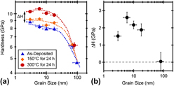
We begin by looking at the effect of grain size on the magnitude of relaxation strengthening in the saturated condition. Figure 5(a) shows hardness as a function of grain size for the as-deposited and annealed Ni–W specimens. Nanoindentation was performed at a constant indentation strain rate of 1.5 × 10⁻¹ s−1 for the results presented in this figure. The hardness data from the as-deposited specimens show the expected breakdown in Hall–Petch scaling for grain sizes below ∼20 nm. After annealing, the hardness grain size trends shift toward higher hardness values, with higher temperature annealing treatments resulting in more strengthening. Of particular interest is the fact that the magnitude of the strengthening effect exhibits a clear dependence on grain size. At the larger grain sizes, no appreciable strengthening is found. The observed strengthening effect increases in magnitude with decreasing grain size down to d = 6 nm. However, when grain size is further reduced to ∼3 nm, the hardening effect becomes less pronounced. These trends can be more clearly seen by plotting the hardness change between the as-deposited and 300 °C heat-treated states (ΔH) as a function of grain size, as shown in Fig. 5(b). Relaxation of grain boundary structure appears to be most influential on hardness at a grain size of ∼6 nm. The existence of a maximum hardening effect at an intermediate grain size is consistent with the previous MD studies of Vo et al.Reference Vo, Averback, Bellon and Caro27 Although the MD simulations of these authors focused on pure nanocrystalline Ni and were carried out at extremely high strain rates, grain boundary relaxation was observed to be most effective for improving the strength at grain sizes of ∼5–7 nm.
(a) Nanoindentation hardness of nanocrystalline Ni–W plotted as a function of grain size for as-deposited specimens, specimens annealed for 24 h at 150 °C, and specimens annealed for 24 h at 300 °C. (b) The difference between the hardness of the as-deposited state and the hardness after annealing for 24 h at 300 °C (ΔH), showing that relaxation hardening is most pronounced at a grain size of ∼6 nm.

To further understand how grain boundary relaxation affects deformation, hardness was measured at seven indentation strain rates between 1.5 × 10⁻² and 15 s−1 to calculate an apparent activation volume, V, for deformationReference Kocks, Argon and Ashby50, Reference Taylor51:
where k B is the Boltzmann constant. This activation volume represents the characteristic volume over which work is done during a thermally activated plastic event and is a signature of the dominant deformation mechanism. Hardness is presented as a function of strain rate in Fig. 6 for the as-deposited and annealed states. Activation volume values, calculated following Eq. (5) and normalized by the cubed Burgers vector (b 3), for both as-deposited and heat-treated specimens are presented in Fig. 7 as a function of grain size.
Hardness as a function of strain rate for as-deposited and annealed specimens with grain sizes from 3 to 75 nm. This data is used to calculate the activation volumes presented in Fig. 7.

Activation volumes for both as-deposited and annealed Ni–W specimens, plotted as a function of grain size. For grain sizes down to ∼10 nm, annealing does not change the measured activation volumes. However, for the finest grain sizes, annealing results in an increase in the activation volume, suggesting a change in the dominant deformation mechanisms for these structures.

For grain sizes in the range ∼10–100 nm, annealing has no observable effect on the measured activation volume values. This suggests that the dominant deformation mechanisms are unchanged by grain boundary relaxation over this range of grain sizes. A widely accepted strength-limiting mechanism that controls deformation in nanocrystalline metals with these grain sizes is the emission of dislocations from grain boundaries, which subsequently traverse the grain. Grain boundary relaxation removes excess grain boundary dislocations, reducing the density of sources available for dislocation emission. Fewer available sources mean that a higher applied stress is necessary to initiate slip, which agrees with our observations of hardening after annealing. However, a change in the source density need not affect the rate-limiting process (mechanism) of plastic flow, which is consistent with the unchanging activation volumes we have measured here.
Our results are very different for grain sizes below ∼10 nm, however, where annealing increases the activation volume over that of the as-deposited state, first through a subtle increase at d = 6 nm (from 20 to 32 b 3 at 300 °C, with no appreciable change observed at 150 °C) then a more pronounced change at d = 3 nm (from 28 to 51 b 3 at 150 °C and to 43 b 3 at 300 °C). This suggests that the strength-controlling deformation event in samples at these finest grain sizes grows upon annealing to involve larger numbers of atoms. In other words, the mechanism of deformation appears to be considerably different after these samples are annealed.
Additional support for a fundamental shift in the deformation physics is provided by another set of indentation tests using a cube corner indenter tip; the sharper cube corner geometry involves less constraint than a Berkovich tip and allows a clearer inspection of the plastic zone on the indented surface. Although changing to a cube corner tip leads to significant pileup that would make accurate hardness measurements more difficult, these experiments were used here to make qualitative observations only. The plastic zones of the residual impressions from these indentations were inspected in the SEM, as shown in Figs. 8(a)–8(c) for the d = 3 nm specimen. In the as-deposited state [Fig. 8(a)], small shear offsets are observed in the plastic pileup surrounding the indentation site. However, the annealed specimens [Figs. 8(b) and 8(c)] exhibit more pronounced, larger shear steps in the pileup.
Scanning electron microscopic images of the residual impressions left after nanoindentation with a cube corner tip into d = 3 nm Ni–W in the (a) as-deposited state, (b) after annealing for 24 h at 150 °C, and (c) after annealing for 24 h at 300 °C. (d) Typical load–displacement curves for as-deposited specimens and after annealing for 24 h at 300 °C. (e) Average strain rate as a function of depth, showing strain bursts for the annealed specimen, which correspond to the discontinuities seen in the indentation response in (d). The shear steps in the pileup become larger and strain bursts are observed after annealing treatments, showing that grain boundary relaxation promotes localized flow in the finest nanocrystalline grain sizes.

Evidence for increased shear localization after annealing can also be found through the inspection of the load–displacement curves presented in Fig. 8(d). While a relatively smooth curve is seen for the as-deposited specimen, a number of small discontinuities are observed in the load–displacement curve for the sample annealed at 300 °C. Figure 8(e) shows the average indentation strain rate as a function of depth for the two curves presented in Fig. 8(d). While the average strain rate fluctuates around the target value (1.5 × 10⁻² s−1), peaks in the strain rate, or periods of rapid indenter travel, are found which correspond to the discontinuities in the load–displacement curve of the annealed sample (the black arrows in Figs. 8(d) and 8(e) denote the same events). These rapid displacement bursts, or periods of high strain rate flow, likely correspond to the shear offsets observed in the plastic pileup. It is important to note that strain bursts were not observed when a Berkovich indenter tip was used, so our measurements of apparent activation volume in Fig. 7 were not affected by the localization described here.
Taken together, our observations of more pronounced shear offsets in the plastic zones and more conspicuous displacement bursts in the indentation curves of annealed samples suggest a shift toward increased flow localization in the relaxed specimens. We interpret this change in terms of the mechanism of atomic shear shuffling that is believed to control plasticity in this grain size range. Nanocrystalline metals with grain sizes below 10 nm deform by collective mechanisms, such as grain boundary slidingReference Schiotz, Di Tolla and Jacobsen11, Reference Van Swygenhoven and Derlet12 and grain rotation,Reference Ke, Hackney, Milligan and Aifantis8–Reference Shan, Stach, Wiezorek, Knapp, Follstaedt and Mao10 which are triggered by local “shear transformation zone”-like activity in the grain boundaries.Reference Lund, Nieh and Schuh52 In an as-deposited material, the excess grain boundary defects act as local stress concentrations and sites for the preferential initiation of these collective movements, resulting in a relatively small activation volume. In a relaxed specimen, the grain boundaries are more homogeneous and ordered, meaning higher stresses are required for plastic deformation, and when plasticity commences, slip initiates over a much larger volume of grain boundary material rather than at specific high-energy sites.
Trelewicz and SchuhReference Trelewicz and Schuh35, Reference Trelewicz and Schuh39 noted the emergence of shear bands in as-deposited nanocrystalline alloys as being reminiscent of the plastic flow of metallic glasses and provided a detailed comparison with glass mechanics to establish the similarities. An interesting aspect of the present results is that the increased propensity for flow localization after structural relaxation is also strikingly similar to the behavior of amorphous metals. For example, Jiang and AtzmonReference Jiang and Atzmon53 found that annealing to increase local order also led to larger flow serrations and an increase in pileup volume during nanoindentation of an amorphous Al alloy. Shi and FalkReference Shi and Falk54 reported a similar effect in MD simulations of nanoindentation of metallic glasses; highly disordered glasses had a tendency to deform via a series of smaller shear bands, where more locally ordered glasses developed larger, more conspicuous shear bands. In both these cases, the relative trend of increased order leading to more pronounced localization is in line with our observations on nanocrystalline samples.
V. CONCLUSIONS
In this article, we have used nanocrystalline Ni–W alloys to explore the kinetics and grain size dependence of grain boundary relaxation strengthening. The results presented here provide insight into what is essentially a new strengthening mechanism that is specifically relevant to nanocrystalline materials. The following conclusions can be drawn:
(i) Grain boundary relaxation occurs at low temperatures and can significantly increase the hardness of nanocrystalline metals. The maximum amount of strengthening which can be realized depends on the annealing temperature, with higher temperature treatments resulting in an enhanced hardening effect. We have recorded strengthening increments of up to 20% to microhardness levels as high as 9.3 GPa.
(ii) The rate of hardening from grain boundary relaxation is a strong function of temperature, with higher temperatures leading to faster hardening. Quantification of this temperature dependence through an Arrhenius law gives an apparent activation energy of about 50 kJ/mol, which may relate to triple junction diffusion. Interestingly, the total amount of hardening achieved once the effect saturates also appears to be temperature dependent for reasons that are not entirely clear.
(iii) The saturation strengthening achievable by grain boundary relaxation demonstrates a significant grain size dependence. No hardening is observed for large nanocrystalline grain sizes, but the magnitude of hardening increases with decreasing grain size until a maximum is observed at d = 6 nm. At the finest grain size below this critical value, grain boundary relaxation strengthening is less pronounced.
(iv) For grain sizes down to ∼10 nm, grain boundary relaxation does not appear to change the dominant physical mechanism for deformation. A reduction in the number of available sources for dislocation emission with annealing can explain the observed strengthening in this regime.
(v) However, for grain sizes below 10 nm, grain boundary relaxation changes the dominant deformation mechanism, which is manifested as an increase in the measured activation volume. Plastic deformation becomes more localized in specimens with the finest grain sizes as grain boundary structure is relaxed.
Taken as a whole, the results presented here show that short, low-temperature annealing treatments can effectively strengthen nanocrystalline metals. Since the thermal treatments discussed here offer a quick, low-energy method by which to significantly improve mechanical properties, we envision that they may become extremely useful in practice as nanocrystalline alloys are integrated into engineering systems. The work presented here delineates the conditions and grain sizes for maximum effectiveness of relaxation strengthening.
ACKNOWLEDGMENTS
This work was supported by the US Army Research Office through Grant W911NF-09-1-0422 and through the Institute for Soldier Nanotechnologies at Massachusetts Institute of Technology.


