


Introduction
The rapid development of the fifth generation (5G) of wireless systems also permeates satellite communications. The integration of satellite and terrestrial networks is probably the key factor in enabling many new services and providing true full coverage. To this end, very high throughput satellites (vHTS) will be deployed, creating new opportunities in the space market [Reference Di, Zhang, Song, Li and Li1]. This family of vHTS can offer high capacity (e.g., 1 Terabit/s per satellite) to a larger number of users, thus allowing for a lower cost per gigabits per second. They also increase the network flexibility and operability, since the satellite service can be allocated when and where it is needed [Reference Giambene, Kota and Pillai2]. Applications like multimedia distribution, machine-to-machine communications, critical telecommunication missions, aero and maritime connectivity, network control signaling, back-hauling, and service continuity are well positioned to be the main contributions of satellites to the 5G ecosystem [Reference Fenech, Amos, Tomatis and Soumpholphakdy3]. Future vHTS will make use of Q/V gateways, where the forward payload link will operate in the K-band (i.e., 17.3–20.2 GHz), usually referred to as the Ka-band satellite downlink [Reference Emrick, Cruz, Carvalho, Gao, Quay and Waltereit4]. The required radio-frequency (RF) power capability in such a bandwidth is about 110 W at saturation, while the number of equipment integrated into the payload is ~150 units. Radio Frequency (RF) power amplifiers (PAs) are one of the key components of a communications satellite's payload, consuming ~80% of the spacecraft available power. Therefore, its efficiency is of the utmost importance. Traditionally, the demand for such a high power level at high frequencies, has resulted in the adoption of traveling wave tube amplifiers (TWTAs) as the preferred choice for transmitter modules. However, technological advances in linearization techniques, miniaturization, and the use of different materials such as gallium nitride (GaN), have leveled the playing field towards the use of solid state PAs (SSPAs). The latter could be an attractive solution to replace K-band TWTAs, although the efficiency of SSPAs is still lower than that of the tube amplifiers. Indeed, aspects such as lower cost, graceful degradation, form factor, etc., can introduce significant benefits at satellite level. In this context, several monolithic microwave integrated circuits (MMICs) PAs have been recently demonstrated up to K/Q band [Reference Fong, Srisathapat, Chin, Telvin, Grebliunas and Wu5–Reference Colantonio and Giofré23].
This paper is an extended version of [Reference Colantonio and Giofré23]. It discusses the design and experimental characterization of an MMIC PA implemented on a 100-nm gate length GaN on silicon (GaN/Si) technology and conceived to be the building block of a space-borne SSPA for vHTS covering the full satellite downlink Ka-band. From 17.3 to 20.2 GHz, the realized MMIC delivers an output power (P out) >40 dBm with a power added efficiency (PAE) peak >40% and 22 dB of power gain.
MMIC design
The MMIC is planned to be integrated in the SSPA RF Tray, by combining 16 of them into a radial combiner [Reference Giofré, Colantonio, Di Paolo, L and Lopez24], with the aim of achieving a total output power of 125 W under continuous wave (CW) operating conditions, while a single MMIC will be used as a driver, as schematically depicted in Fig. 1. The complete RF tray includes a gain control unit, embedding linear amplifiers, analog variable attenuators, and an analog linearizer, to assure an overall RF gain >70 dB with proper thermal/aging compensation features.
Schematic architecture of the SSPA. (a) Simplified scheme of the SSPA RF tray. (b) Radial combiner solution integrating 16 packaged MMICs.

The MMIC is implemented in the commercially available 100-nm gate length GaN-Si process available in OMMIC foundry (D01GH process) [25].
Considering the lower thermal conductivity of Si as compared to that of the standard silicon-carbide (SiC) typically adopted in GaN processes [Reference Boles26], a careful technology assessment and power budget analysis was initially carried out. In addition, an accurate thermal evaluation of the technology was performed by using Raman measurement [Reference Ramella, Pirola, Reale, Ramundo, Colantonio, Maur, Camarchia, Piacibello and Giofrè27].
Technology assessment
A load-pull analysis was carried out on different devices’ periphery, assuming a drain bias voltage V DD = 11.25 V and a preliminary quiescent drain current of 75 mA/mm (class AB bias condition, as tradeoff for power and PAE). The aim was to identify the most suitable MMIC architecture, together with the size of the devices and their loading impedances, taking into account space constraints. Clearly, the device's channel temperature (T j) was carefully monitored assuring that its value did not exceed the upper limit of 160°C, in the worst-case condition. In particular, since the MMIC has to operate in CW conditions over a temperature range from –10 to 65°C at the SSPA level, which implies a temperature T BS up to 85°C at the MMIC backside, the $\varDelta \, T = T_j-T_{BS}$ in the MMIC has to be kept < 75 °C.
The load pulls were performed at the fundamental frequencies f c in the frequency range from 17.3 to 20.2 GHz. An example is reported in Fig. 2 for the 8 × 100 μm device. Notably, together with the standard contours of output power (blue curves), efficiency (red curves), and gain (green curves), it is also reported the curve corresponding to T j = 160 °C (i.e., brown curves, safe area inside). The optimum load of $\Gamma _{opt} = 0.69\cdot e^{j153^\circ }$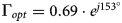 was selected as a tradeoff among output power, efficiency and gain, provided that the limit on T j was respected.
Load pull for the 8 × 100 μm device for the carrier frequencies of 17.3, 19.3, and 20.2 GHz. The input power is 24.7 dBm. The blue contours refer to the output power, green to the gain, red and brown to the drain efficiency and junction temperature, respectively.

The effect of the impedance at the second harmonic (2f c) was also investigated. In particular, the second harmonic load-pull reveals a critical region (close to the short-circuit condition) where is experienced a severe drop in the device performances. Fig. 3 shows the obtained behaviors for the 8 × 100 μm device, but a similar one was registered for all devices. As a countermeasure, this region was carefully prevented for all devices in the design of their matching networks.
Load-pull results performed with the fundamental frequency 18.75 GHz and P in = 24.7 dBm and varying the phase of the second harmonic (37.5 GHz) for the 8 × 100 μm device: (a) reports the simulated output power (blue curve, left axis) and power gain (red curve, right axis); (b) the corresponding estimated channel temperature (red curve, left axis) and power added efficiency (green curve, right axis); (c) the loading condition assumed at 37.5 GHz, are represented by the black points, while the critical region to be avoided is represent by the red circles. (a) Output power and gain, (b) efficiency and junction temperature, and (c) critical area.

The main features of each analyzed device were evaluated at 2 dB of gain compression, together with the corresponding T j in the worst-case conditions (i.e., T BS = +85°C). The results are summarized in Fig. 4. As it can be noted, a power gain of about 9 dB can be obtained from the active devices, with an almost similar PAE of ~60%, with a power capacity that increases with the device active periphery, as expected.
Output power, associated gain, and PAE at 2 dB of gain compression together with the correspondent channel temperature T j, simulated at center frequency 18.75 GHz for different device geometries.

Amplifier architecture
Relying upon the outcomes of the preliminary analysis and accounting for thermal, electrical, and physical constraints of the technology, a three-stage corporate architecture was chosen. Its block diagram is shown in Fig. 5. The final stage is based on the parallel combination of eight 8 × 100 μm devices, each providing ~33 dBm and 8.0 dB of output power and gain, respectively (see Fig. 4). The driver stage includes four 6 × 100 μm devices (thus, one device 6 × 100 μm in the driver stage driving two devices 8 × 100 μm in the final stage), whereas a pre-driver stage realized by two 4 × 100 μm devices (i.e., still 1:2 splitting) was also adopted in order to fulfill the overall gain requirement.
Architecture of the HPA MMIC. For the networks, it has been preliminary estimated a power loss of 1 dB for the output combiner and 1.5 dB for both the interstage matching networks.

To simplify the MMIC interconnections, the same dc biasing voltage, i.e., V DD = 11.25 V, V GG = −1.65 V, was adopted for all the stages. It corresponds to a quiescent current of 35, 27, and 18 mA for each device in the final, driver, and pre-driver stages, respectively. This choice is the result of a tradeoff between electrical performances and maximum allowed temperature at the device level. In particular, the imposed condition was that the quiescent bias point was below the curve of maximum allowed power dissipation.
Design steps
Preliminary, all the devices used in the amplifier were made unconditionally stable from dc up to 90 GHz, by adding a standard resistance–capacitance (R–C) stabilization network on the gate path and a resistor in a series on the dc gate biasing access point, if required. Subsequently, the actual implementation of the MMIC started. As the first step, the output combiner was designed accounting for the optimum loads inferred by load-pull simulations on the 8 × 100 μm device, which are reported in Fig. 2. This network was synthesized using a three-section structure, as shown in Fig. 6(a). The load presented across each device is reported in Fig. 6(b) together with the trajectory plotted for both the fundamental frequency and the second harmonic, in a larger carrier frequency range from 17 to 21 GHz. The structure was tailored to allow the possibility to bias the MMIC on both sides (i.e., top and bottom). Moreover, the size of the transmission lines was properly optimized to reduce losses, while simultaneously assuring the capability to withstand the amount of dc current required by all devices under large signal conditions.
Designed output combiner (a) and synthesized load (b). The power losses result in ~0.8 dB (c). (a) Output combiner. (b) Synthesized loads. (c) Combiner loss.

The designed combiner exhibited ~0.8 dB of losses, as reported in Fig. 6(c). The resulting performance obtainable from the final stage alone, assuming a T BS = 85°C, is reported in Fig. 7 together with the T j behavior of the device. The latter was evaluated relying upon the electrothermal model provided by the foundry, as discussed in [Reference Ramella, Pirola, Reale, Ramundo, Colantonio, Maur, Camarchia, Piacibello and Giofrè27].
Simulated performance of the final stage alone, when each device is driven with 24 dBm of input power at its gate.

Hence, a similar approach was adopted to design the remaining interstage matching networks represented in Fig. 5. The results of the load-pull simulation of the involved devices, i.e., 6 × 100μm and 4 × 100 μm for the driver and pre-driver stages, respectively, are shown in Fig. 8(b).
Simulated load pull for the devices used in the driver (a) and pre-driver (b) stages. The former is 6 × 100 μm, the latter 4 × 100 μm, both biased with V DD=11.25 V and quiescent current I D=27 mA and I D=18 mA, respectively. The contour plots refer to 1 dB of gain compression.

Also in these cases, the matching networks were designed assuring the possibility to bias the devices from both sides. For the interstage between driver and final devices, a load transformation from the input impedance (Z in) shown by the 8 × 100μm in the final stage to the optimum impedance (Z L) required by the 6 × 100μm device in the driver stage was performed, as shown in Fig. 9, for the bias condition V DD = 11.25 V, I D = 27 mA and I D = 18 mA for the 6 × 100 μm and 4 × 100 μm devices, respectively. The load pulls are computed at 1 dB of gain compression (i.e., correspondingly to P in = 24.5 dBm for device 6 × 100 μm and P in = 20.1 dBm for device 4 × 100 μm).
Designed interstage matching network between driver and final stages (a) and synthesized load (b). The insertion loss is within 1 and 1.5 dB (c). (a) Interstage matching network between one driver and two final devices. (b) Synthesized loads. (c) Combiner loss.

Similarly, the impedance transformation as well as the synthesized matching network between the pre-driver and the driver devices are reported in Fig. 10. In this case, the losses were between 1 and 1.5 dB in the bandwidth.
Designed interstage matching network from one pre-driver to two driver devices (a) and synthesized load (b). The power losses result within 0.8-1.3dB (c). (a) Interstage matching network between one pre-driver and two driver devices. (b) Synthesized loads. (c) Combiner loss.

The MMIC was completed by designing the input matching network to transform the input impedance of the two devices used in the pre-driver into the standard termination of 50 Ω. The structure was fine re-tuned by means of electromagnetic simulations of the entire passive structures. Finally, the odd-mode and parametric oscillations were analyzed by referring to Ohtomo test [Reference Ohtomo28] and by using the STAN tool (pole-zero analysis package described in [Reference Dellier, Mori, Collantes, Anakabe and Campbell29]). The former, based on the evaluation of loop gains, requires avoiding the encirclement of the point (1,0), as reported in Fig. 11. The latter, is based on the analysis of pole-zero loci of the transfer function obtained by perturbing each gate/drain of the 14 devices in different power conditions, verifying that there are no real half-plane poles for all power levels.
Loop gain simulated by using the Ohtomo test [Reference Ohtomo28], for the frequency from 100 MHz up to 80 GHz. The condition for stable loop is fulfilled if none of the loop gain encircles the point (1, 0) shown in the figure.

The photo of the realized amplifier is shown in Fig. 12 (size 5 × 4.4 mm2).
Photo of the realized amplifier (size 5 × 4.4 mm2).

Simulation results
The simulated small-signal performances of the designed MMIC are shown in Fig. 13. The gain (S 21) is around 19 dB with an input/output matching better than 15/10 dB.
Simulated small-signal S-parameter.

The large-signal performances as a function of the input power, for the frequency range from 17.3 to 20.2 GHz, are reported in Fig. 14(a). In the same figure are also reported the output power delivered by the devices in the driver (Po_D) and pre-driver (Po_PD) stages, respectively, which operate in almost linear conditions. This is also confirmed by the dynamic load lines of the devices, simulated across the intrinsic current source, reported in Fig. 15. For a fixed input power of 20 dBm, i.e., identified as the nominal operating point of the amplifier, the corresponding simulated frequency behavior is reported in Fig. 14(b). As it can be noted, a PAE higher of 35% is achieved with an output power of 40 dBm (10 W) and a gain of 20 dB in the target bandwidth (highlighted in the same figure).
Simulated performance: (a) as a function of the input power for the carrier frequencies from 17.3 to 20.2 GHz; (b) over frequency for a fixed input power level P in = 20 dBm. (a) Power sweep. (b) Frequency sweep.

Load lines for the devices in the pre-driver (a), driver (b), and final stages (c), respectively, simulated for P in=20 dBm.

Fig. 16 shows the thermal map of the chip obtained by running an electro-thermal simulation (by using HeatWave simulation tool from Keisight) assuming a base plate temperature of 85°C and also taking into account for the R TH of the mounting stack. As expected, the hottest devices are those in the final stage, and the highest temperature is reached at the center of the devices. Nevertheless, the maximum temperature does not exceed the limit of 160°C.
Simulated thermal map of the designed MMIC, assuming T BP = 85°C and for the overall stack (below MMIC) a thermal resistance R th,stack = 0.28°C/W. (a) Two-dimensional view at MMIC level; (b) Three-dimensional view to see the temperature spread in the vertical section.

Measurement results
The chip was initially characterized on-wafer in pulsed condition (pulse repetition time 10 μs with 1% duty cycle) and in both small- and large-signal conditions. The small-signal performances measured from several MMICs at the nominal bias conditions are reported in Fig. 17 together with the simulations. A frequency shift of about 500 MHz towards lower frequencies was registered. Nevertheless, a small-signal gain (S 21) close to 25 dB was registered, with an input/output return loss better than 7 and 5 dB, respectively, and with a negligible variation among all the measured chips. The difference between the measured and simulated gains is essentially related to the pulsed condition and the inaccuracy of the active device model in predicting small-signal behavior as compared to non-linear situations (as highlighted later).
Comparison between simulated (dash) and measured scattering parameters of 10 samples. (a) S 11, (b) S 21, and (c) S 22.

The MMICs were then characterized on-wafer under large-signal conditions, in the same pulsed condition and at the nominal bias point, i.e., V DD=11.25 V with total bias currents of 30, 110, and 300 mA for the three stages, respectively. The measured output power, gain, and PAE (continuous lines) are reported in Fig. 18, compared with the simulated counterparts (dashed lines).
Comparison between simulated (dashed lines) and measured (continuous lines) power performances. The latter refers to the same MMIC version located in different wafer positions, to test the reproducibility of the results on the wafer.

Notably, in this case, the model prediction is closer to the measured results, even if a slightly higher P out was obtained under pulsed condition. Specifically, an output power in excess of 40 dBm (10 W) together with a PAE above 34% (peak of 39% in the middle of the bandwidth) and a gain larger than 22 dB were recorded in the frequency range from 17.3 to 20.2 GHz.
The MMIC was then tested under CW operations. However, at this stage, the chosen assembly was not optimized and is intended to provide only a quick information concerning electrical performance. In particular, the die was mounted using epoxy glue and, as shown in Fig. 19, the test jig was made of copper, while all the MMIC gate pads were collapsed on a single external access point, available on both sides. The same for the drain pads.
(a) MMIC mounted in the package. (b) Zoom on the MMIC area.

The amplifier was characterized under CW conditions by using a Peltier cell to control the base plate temperature.
The small-signal behavior measured at the nominal bias point, with a T BP = 25°C is shown in Fig. 20. In the same figures are also reported the performances obtained with a lower voltage V DD = 9 V, showing almost the same behavior.
Small-signal measured results in CW condition. The reference ports are the test-jig input/output RF ports (i.e., SMA connectors) and TRL calibration was considered.

The large-signal performance measured at the nominal bias point in CW and at 4 dB of gain compression, i.e., with a fixed input power of ~15 dBm, are reported in Fig. 21, without applying any compensation for the bond wires and lines used to connect the MMIC to the package. An output power >39 dBm was obtained between 18 and 20 GHz, with a power added efficiency close to 30%, which is the highest value reported in this frequency range for GaN-Si devices.
Measured CW performance of the packaged MMIC (black lines are the simulation at MMIC level). The bias point is V DD=11.25 V and total current absorption of 1 A, with P in=15 dBm.

The packaged MMIC was also characterized over temperature, by controlling the latter at the bottom of the test-jig with a Peltier cell, and changing the reference temperature from 20 to 40°C and 60°C. Taking into account the thermal resistance of the material stack (i.e., package and epoxy glue), which implies approximately a 25°C of the temperature increase, at the backside of the MMIC the estimated temperature results to be about 45, 65, and 85°C, respectively. The measured results are reported in Fig. 22, where the input power level is kept constant in all cases. As it can be noted, the variation of the performances is limited.
Measured CW performance of the packaged MMIC at the nominal bias point and for different temperatures.

Finally, the performances of the realized MMIC are compared with state-of-the-art results in the same frequency range given in Table 1 and graphically in Fig. 23. Notably, the results achieved with the GaN/Si technology used in this design and, above all, accounting for de-rating and temperature constraints, which pose severe challenges during the design phases, compared pretty well with those obtained using GaN/SiC technologies. Consequently, the reported results demonstrate the ability of GaN/Si technology to be a valid alternative to GaN/SiC technology also for spacecraft applications.
State-of-the-art comparison.

Comparison with other GaN MMICs PAs

$^{\rm {a}}T_{BS} = 35^\circ {\rm C}$ .
.
$^{\rm {b}}{\rm Packaged,\; \ 5\, dBc,\; \textit {T}_{\textit {BP}} = 90}^\circ {\rm C}.$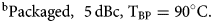
$^{\rm {c}}$ Doherty configuration.
$^{\rm {d}}$ Packaged.
Conclusion
In this paper, the design and experimental results of an MMIC PA developed on the 100-nm gate length GaN-Si commercial process (D01GH from OMMIC) have been discussed. The PA has been designed to operate in the frequency range from 17.3 to 20.2 GHz for space applications, and in particular for the next generation K-band vHTS spacecraft. Accounting for space de-rating rules and severe temperature constraints, an output power larger than 40 dBm with a power added efficiency above 30% (with a peak higher than 40%) and 22 dB of power gain have been demonstrated with pulsed measurement at on-wafer level. The MMIC has been then assembled in a preliminary carrier (not fully optimized) for the CW characterization. The latter demonstrates quite stable performances over a large temperature range, showing an output power and PAE larger than 39 dBm and 28%, respectively, at 85°C of the backside temperature.
Acknowledgments
This project was received funding from the European Union's Horizon 2020 Space Research and Innovation Program under grant agreement no. 821830.
The authors are grateful to OMMIC for performing the on-wafer characterization.
 Paolo Colantonio (SM’18) received the M.S. degree in Electronics Engineering from the University of Roma Tor Vergata in 1994 and the Ph.D. degree in Microelectronics and Telecommunications in 2000. He is a full professor of Microwave Electronics at the University of Roma Tor Vergata. His research activities are mainly focused on the field of microwave and millimiter-wave electronic, and in particular on the design criteria for non-linear microwave subsystems and high efficiency power amplifiers. He has published over 270 scientific papers, is an author of a book on solid-state power amplifiers (High Efficiency RF and Microwave Solid State Power Amplifiers, Wiley, 2009), three book chapters, four contributions on Encyclopedia of RF and Microwave Engineering (Wiley), and two patents. He is an author or a coauthor of more than 250 scientific papers. He authored the book High Efficiency RF and Microwave Solid State Power Amplifiers (Wiley, 2009), three book chapters, four contributions to Wiley Encyclopaedia on Microwave Electronics and one international patent.
 Rocco Giofrè (SM’14) received the M.S. degree in Electronic Engineering (summa cum laude) from the University of Roma Tor Vergata, Rome, Italy, in 2004, and the Ph.D. degree in Space Systems and Technologies from the University of Roma Tor Vergata in 2008. He is currently an Associate Professor with the University of Roma Tor Vergata. He has authored or coauthored more than 150 scientific papers and two contributions to Wiley Encyclopaedia on Microwave Electronics and one international patent. His research interests include RF power amplifier theory, design and test, linearization techniques, and efficiency improving techniques. Dr. Giofrè was the recipient of the 2005 Young Graduated Research Fellowship presented by the GAAS and of the Best Paper Award at the Second EuMIC Conference in 2007.
 Fabio Vitobello received the Power Electronics Engineering degree cum laude from the University of Padova, Padova, Italy, and a double degree from the Illinois Institute of Technology (IIT), Chicago, IL, USA, with a major in Microelectronics Engineering. He performed research activities on GaN HEMT devices at the IIT until 2007. In 2008, he joined the European Space Agency (ESA), Paris, France, where he was involved in the development of European Space compatible GaN RF HEMTs processes and monolithic microwave integrated circuits (MMICs). He was responsible until 2015 for the ESA RF and Microwave Laboratory where he performed many activities, in terms of performance and reliability assessments, related to the Space missions and technology developments. He is currently working in the Space Unit of the Research Executive Agency, part of the European Commission as a Program Officer. His research interests include the design and reliability aspects of RF and Power GaN HEMTs, MMICs with a particular attention to space qualifications.
 Mariano Lòpez is a senior RF engineer, graduated in telecommunications engineering in 1997 by the University of Cantabria (Spain), and working for the TTI since 2000. Before, he was working as a RF engineer in the Communications Department of the University of Cantabria. He has been the manager of several R&D and commercial projects in the RF domain, devoted to develop customized equipment as RF transceivers, SSPAs, low noise amplifiers, etc. based on customer requirements at different frequency bands, from L to Ka.
 Lorena Cabrìa received the Telecommunications Engineering and the Ph.D. degrees (with and Extraordinary Doctoral Prize) from the University of Cantabria, Santander, Spain, in 2001 and 2007, respectively. Between 2001 and 2011, she worked as a Research Associate in the RF and Microwave Group at the University of Cantabria. Currently, she is working as a project manager at the TTI, Santander, Spain. Her main research interests include RF and microwave integrated circuits, intermodulation distortion control on RF and microwave applications, high efficiency power amplifiers, emerging wireless transmitter architectures and the development of SSPAs for particle accelerators and for satellites.


 Open access