













Introduction
The transition from fifth-generation (5G) to sixth-generation (6G) wireless/mobile networks, or more precisely, the enhancement of 5G through the incorporation of advanced 6G technologies, necessitates a significant commitment in terms of effort and investment. Experts have projected that 6G will be allocated within the upper mid-range spectrum. In this context, leveraging the existing below-6-GHz mobile cell infrastructure, the new frequency bands must contend with increased path loss and more challenging propagation conditions. Furthermore, 6G aspires to substantially broaden coverage for non-terrestrial links, which are similarly affected by heightened propagation losses. As a result, the implementation of reconfigurable intelligent surfaces (RISs) emerges as a promising strategy to enhance link performance within 6G mobile networks [Reference Saad, Bennis and Chen1].
An RIS can manipulate the phase of incident electromagnetic waves through its programmable elements, thereby steering reflected signals toward desired directions. This capability enables non-line-of-sight links to be effectively transformed into virtual line-of-sight paths via controlled reflections [Reference Wu and Zhang2]. In full-duplex communication scenarios, RISs are required to support dual polarization, as simultaneous transmission and reception often rely on two orthogonal polarization channels to improve self-interference cancellation (SIC) [Reference Tohidi, Askar, Utkovski and Stańczak3]. Moreover, dual-polarized RIS architectures are particularly attractive for Integrated Sensing and Communication (ISAC) systems [Reference Chepuri, Shlezinger, Liu, Alexandropoulos, Buzzi and Eldar4], which represent a key pillar of 6G networks. For such applications, the most critical design requirements include minimal polarization conversion – equivalently, high cross-polarization isolation (XPI) – and independent control over both polarization channels [Reference Kim, Yang, Kim and Oh5]. High isolation ensures interference-free operation between polarization channels, thereby enhancing both communication reliability and sensing performance.
In recent years, dual-polarized RISs have been extensively investigated using various phase-shifting technologies, including liquid crystal [Reference Neuder, Liu, Dzieia, Wang and Jiménez-Sáez6], positive-intrinsic-negative (PIN) diodes [Reference Sangmahamad, Janpugdee and Zhao7–Reference Yang, Zhong, Wang, Yan, Jia, Liu, Liu and Gong11], and varactor diodes [Reference Rains, Kazim, Tukmanov, Zhang, Abbasi and Imran12–Reference Liu, Shi, Zhang, Chen, Chen, Yi and Zhang14]. Several design strategies have been proposed in the literature to enhance the XPI. In [Reference Zhu, Han, Li, Ma, Xia, Zheng, Liu and Li9], orthogonally arranged dipoles combined with a crossover structure are employed, resulting in an XPI improvement up to  $25\,\mathrm{dB}$. A cross-shaped slot integrated into the main radiator is used in [Reference Yang, Zhong, Wang, Yan, Jia, Liu, Liu and Gong11] to suppress cross-polarized components, achieving an XPI of approximately $30\,\mathrm{dB}$. A $180^{\circ}$ hybrid coupler placed in the middle layer of a guided-wave-inspired structure provides an XPI level of $23\,\mathrm{dB}$. In [Reference Rains, Kazim, Tukmanov, Zhang, Abbasi and Imran12], a modified particle swarm optimization algorithm is adopted to maximize XPI, yielding an isolation level of about $20\,\mathrm{dB}$.
In this study, one of the SIC techniques – antenna passive cancellation based on polarization mutual orthogonality [Reference Yurtoglu and Askar15, Reference Yurtoglu, Askar, Leather and Peter16] – is employed to enhance the XPI by utilizing a diagonal unit-cell topology. The unit cell is designed to operate in the upper mid-band ( $7.125$– $24.25\,\mathrm{GHz}$), as this band is considered a strong candidate for 6G systems due to the limited data rates achievable in Frequency Range 1 (FR1, below $7.125\,\mathrm{GHz}$) and the high propagation losses associated with Frequency Range 2 (FR2, $24.25$– $52.6\,\mathrm{GHz}$). Consequently, the upper mid-band offers a favorable balance between bandwidth availability and propagation characteristics. The simulated and measured results show that the unit cell achieves a phase shift range of $270^{\circ}$ at the center frequency of $15\,\mathrm{GHz}$ and exhibits high cross-polarization suppression performance, while requiring a minimal number of phase-tuning components (i.e., two varactor diodes per cell) compared with existing RIS designs.
An earlier version of this paper was presented at EuMW 2025 and was published in its Proceedings [Reference Yurtoglu, Askar, Wittig, Schmieder, Peter and Keusgen17]. This journal builds upon the preliminary study by providing a comprehensive and systematic analysis of the proposed unit-cell architecture, detailed RIS simulations, and reflection-coefficient measurements of a fabricated prototype. The remainder of this paper is organized as follows. The second section describes the proposed unit-cell topology and explains its operational principles. The third section presents the RIS simulations under both normal and oblique incidence. The fourth section details the experimental validation of the unit cell. Finally, the fifth section provides the concluding remarks.
Unit cell design and simulation
Topology
As previously mentioned, the RIS can employ dual-polarization capability with high XPI, enabling its use in full-duplex or ISAC systems. Therefore, the unit cell of the RIS must also be dual-polarized, and the reflection phase of each polarization state must be controlled independently. To minimize the complexity of the reflection-phase control, the unit-cell behavior should remain as similar as possible for both polarizations. Considering the scalability requirements of the RIS, the number of phase-tuning components per unit cell must be kept to a minimum to reduce overall cost.
Using a single varactor diode might be sufficient to realize a dual-polarized cell [Reference Farashahi, Seet and Li18]; however, the reflection-phase control would then be joint, meaning the reflection phases of the two polarizations could not be tuned independently. Moreover, the cell’s reflection characteristics may vary with polarization. Thus, achieving independent control for both polarization states requires at least two varactor or PIN diodes. A geometric constraint of using two diodes is that they cannot be placed at the center of the unit cell, as they would physically overlap. To address this, a radiator can be positioned at the center, with two parasitic elements placed at the edges and connected to the main radiator via diodes [Reference Sangmahamad, Janpugdee and Zhao7, Reference Rains, Kazim, Tukmanov, Zhang, Abbasi and Imran12]. With this configuration, both polarization states can be controlled independently while maintaining the minimum number of diodes. However, because both polarizations share the same main radiator, the XPI may not be sufficiently high for full-duplex or ISAC applications. To increase XPI while preserving independent controllability and keeping the number of varactors at a minimum, the radiators for each polarization can be separated and placed side by side [Reference Ke, Dai, Chen, Wang, Zhang, Tang, Yang, Liu, Li and Lu19]. A similar approach, which overlaps vertically and horizontally polarized unit cells to realize a dual-polarized configuration, is presented in [Reference Oh, Jeong, Park and Wi20]. To ensure half-wavelength spacing between same-polarization radiators and to minimize inter-element coupling, we propose a diagonal unit-cell topology, as shown in Fig. 1(a). In this topology, the vertically polarized and horizontally polarized radiators are positioned diagonally, each occupying a quarter-wavelength sub-cell, while the overall unit-cell size remains half a wavelength. Additionally, two dummy dual-polarized radiators can be placed on the opposite diagonal to reduce reflection loss, as they also contribute to radiation for both polarization states. Note that the vertical and horizontal radiators are the ones independently controlled via varactors. Since they are spatially separated and mutually orthogonal, the XPI level can be further improved. A diagonal arrangement of vertically and horizontally polarized elements is also presented in [Reference Venneri and Costanzo21], although it is intended for fixed or static (non-reconfigurable) RIS applications.
Unit cell configuration and design: (a) topology, (b) perspective view, and (c) expanded layers of the structure.

Figure 1 Long description
The first diagram (a) shows a unit cell topology with four quadrants: dual polarized radiator, vertical polarized radiator (tunable), horizontal polarized radiator (tunable) and another dual polarized radiator. Each quadrant is labeled with lambda subscript 0 over 4 and lambda subscript 0 over 2 dimensions. The second diagram (b) presents a perspective view of the unit cell, featuring an air box, Floquet port, varactor diodes and biasing lines. It includes Floquet modes labeled as TE and TM, with arrows indicating electric and magnetic fields. The third diagram (c) displays expanded layers of the structure, including a ground plane, Rogers RO4350B, Rogers RO4450F and metal components. It highlights dimensions such as h subscript 1, h subscript 2, h subscript 3 and various labeled distances and angles. Insets show detailed views of specific components with labels like L subscript b, s subscript w and d subscript i.
Design
Figure 1(b) shows the structure of the dual-polarized unit cell based on varactor diodes and the topology described in the previous section. The size of the unit cell is  $10\,\mathrm{mm} \times 10\,\mathrm{mm}\, (p\approx\lambda_0/2$ at $15\,\mathrm{GHz}$). The horizontally and vertically oriented bow-tie elements serve as controllable horizontally and vertically polarized radiators, while the square patches serve as dummy dual-polarized radiators. Slots are introduced into the bow-tie elements to reduce their electrical size without changing their resonant frequency, thereby enabling them to fit within the quarter-wavelength sub-cell. In addition, square-ring structures are placed around the bow-tie elements, as they modify the slope of the phase curve and enhance the phase-shift range, similar to the effect of an annular ring [Reference Tolin and Bahr22]. Vertical interconnect access (via) holes are placed to bias the varactor diodes with DC voltages.
Figure 1(c) illustrates the layer structure of the unit cell, which consists of three dielectric layers and four metallic layers. The top and bottom substrates are Rogers RO4350B (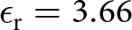 $\epsilon_\mathrm{r}=3.66$, $\tan\delta=0.004$, $h_1=h_3= 0.762\,\mathrm{mm}$). These substrates are bonded using Rogers RO4450F (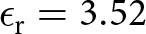 $\epsilon_\mathrm{r}=3.52$, $\tan\delta=0.004$, $h_2= {0.1}\,\mathrm{mm}$), which serves as the middle dielectric layer. The bottom side of the top substrate is a fully metalized ground plane, except for the clearances around the via holes. The vias in the top substrate connect the bow-tie arms, and their associated varactor-diode pads, to the top metallic layer of the bottom substrate, which acts as a filtering layer. A radial stub is implemented on this layer to suppress or minimize RF current leakage before the signal is passed to the bottom layer, which contains all DC routing lines. Without this filtering stage, the RF power could couple into the DC supply network, potentially causing damage. Table 1 lists the dimensions of the proposed unit cell.
Unit cell dimensions

Table 1 Long description
This table presents the dimensions of unit cells for various structures, including substrates, square rings, patches, bow ties, slots, and lines. The substrate has a thickness of 0.762 millimeters, while the bow tie structure features a length of 2.3 millimeters. The square ring and patch have a width of 4.8 millimeters, and the bow tie includes slots with dimensions ranging from 0.1 to 0.9 millimeters. The line and radial stub have a length of 2 millimeters, and the angle of the slots on the bow tie is 70 degrees. These measurements are crucial for understanding the structural differences and potential applications of each design.
Analysis
Electromagnetic simulations of the proposed unit cell were performed in ANSYS® HFSS™ (High-Frequency Structure Simulator) using a Floquet port excitation placed on top of the air box. Two modes (TE, TM) were assigned to the Floquet port (see Fig. 1(b)). In the given coordinate system, the TE mode excites the vertically oriented bow-tie (along the  $y$-axis), while the TM mode excites the horizontally oriented bow-tie (along the $x$-axis). Furthermore, periodic boundary conditions were applied to the side walls of the air box to satisfy the periodicity of the infinite array. A MACOM® MAVR-000120-14110P varactor diode was selected as the phase-tuning component and modeled using a lumped RLC boundary condition. The varactor’s equivalent circuit parameters and physical dimensions were obtained from the manufacturer’s datasheet.
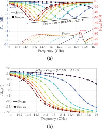
Figure 2(a) shows the magnitude of the unit cell’s reflection coefficient under broadside illumination for various varactor capacitance values ranging from 0.2 to  ${0.9}\,\mathrm{pF}$ in ${0.1}\,\mathrm{pF}$ increments. The left $y$-axis represents the co-polarized reflection (i.e., the incident and reflected modes are the same, $S_\mathrm{TE,TE}$ or $S_\mathrm{TM,TM}$), whereas the right $y$-axis corresponds to the cross-polarized reflection (i.e., the incident and reflected modes are orthogonal, $S_\mathrm{TM,TE}$). It can be observed that the reflection loss is approximately $4.5\,\mathrm{dB}$ within the 14– ${16}\,\mathrm{GHz}$ band, while the XPI exceeds $55\,\mathrm{dB}$. Similarly, Fig. 2(b) illustrates the co-polarized reflection phase for the same capacitance range. A phase shift of $270^{\circ}$ is achieved within the 14.8– ${15.2}\,\mathrm{GHz}$ band, enabling the use of a 2-bit phase resolution to quantize the desired RIS phase distribution. The bandwidth is even larger for a 1-bit phase resolution (i.e., a $180^{\circ}$ phase difference), reaching approximately $1.5\,\mathrm{GHz}$. Owing to the varactor diode’s continuous tuning capability, a 1-bit phase resolution can be achieved at any frequency within this bandwidth by applying appropriate DC bias voltages. In summary, the 2-bit phase-resolution bandwidth is ${400}\,\mathrm{MHz}$ under far-field illumination, whereas the 1-bit phase-resolution bandwidth extends to $1.5\,\mathrm{GHz}$ in near-field RIS deployments, as 1-bit coding suffers from symmetric-beam effects in far-field scenarios [Reference Da Silva, Chu, Xiao and Cerqueira23]. The varactor diode’s capacitance range may limit the achievable phase-shift range. A higher capacitance ratio can increase the phase range. On the other hand, reduced substrate thickness can also extend the phase range, but this may introduce a trade-off by increasing phase slope, reducing bandwidth, and increasing reflection loss. Therefore, the proposed unit cell is designed to balance this trade-off.
Reflection coefficient of the unit cell: (a) magnitude and (b) phase.

Figure 2 Long description
The image A shows a graph of reflection coefficient magnitude versus frequency in gigahertz. The x-axis is labeled 'Frequency (GHz)' and the y-axis is labeled '[S subscript nm] (dB)'. Two curves are plotted: S subscript TE,TE (solid line) and S subscript TM,TM (dashed line). The capacitance values range from 0.2 to 0.9 picofarads. The reflection loss is approximately 4.5 decibels within the 14 to 16 gigahertz band, while the cross-polarized reflection exceeds 55 decibels. The image B shows a graph of reflection coefficient phase versus frequency in gigahertz. The x-axis is labeled 'Frequency (GHz)' and the y-axis is labeled 'L S subscript nm (degrees)'. Two curves are plotted: S subscript TE,TE (solid line) and S subscript TM,TM (dashed line). The capacitance values range from 0.2 to 0.9 picofarads. A phase shift of 270 degrees is achieved within the 14.8 to 15.2 gigahertz band, enabling a 2-bit phase resolution. The bandwidth is larger for a 1-bit phase resolution, reaching approximately 1.5 gigahertz.
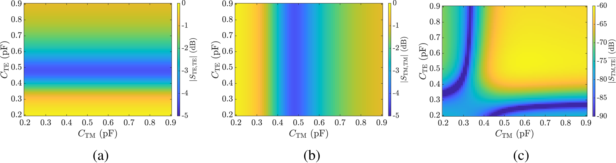
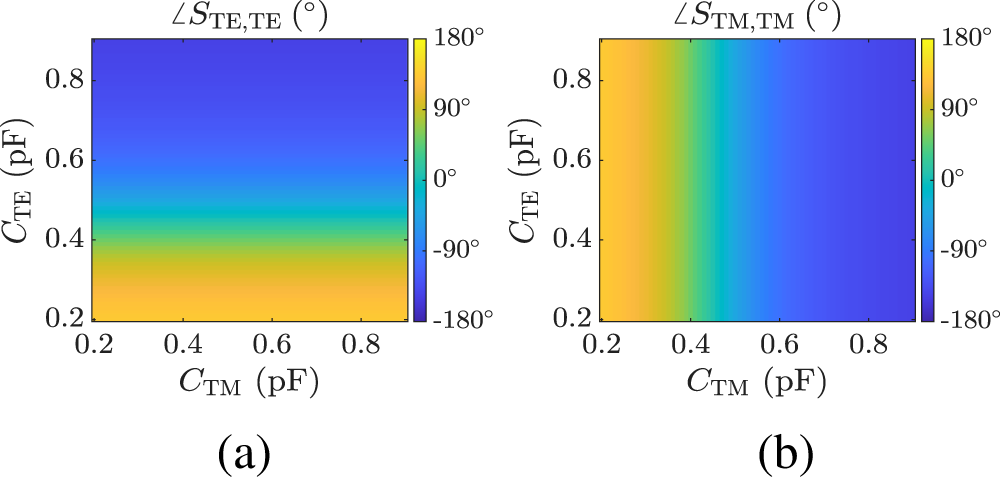
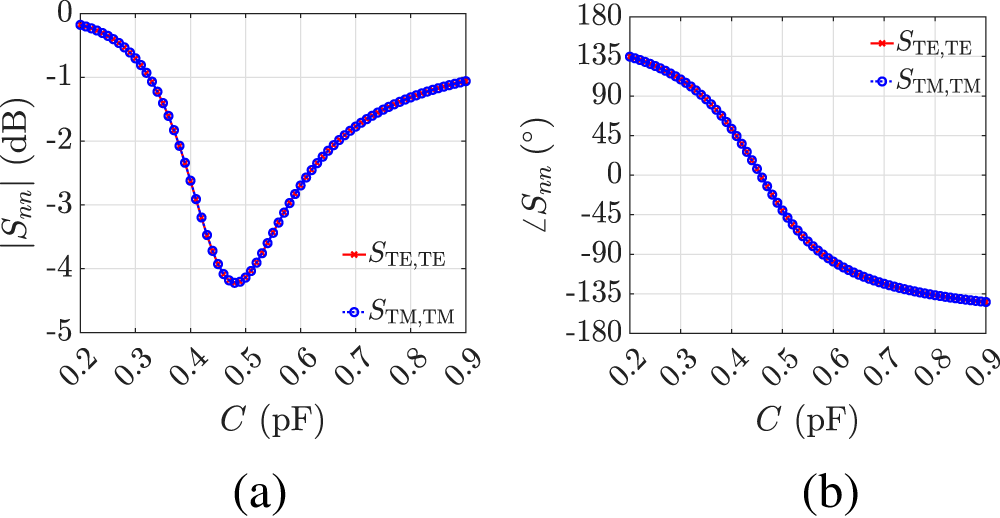
Figure 3(a) and (b) shows the  $|S_\mathrm{TE,TE}|$ and $|S_\mathrm{TM,TM}|$ responses of the unit cell for various capacitance combinations of the vertical and horizontal varactor diodes at the center frequency of $15\,\mathrm{GHz}$, respectively. The maximum reflection loss is approximately $4.2\,\mathrm{dB}$. On the other hand, XPI is more than $61\,\mathrm{dB}$ for all capacitance combinations as illustrated in Fig. 3(c). Similarly, Fig. 4(a) and (b) shows the phase of the co-polarized reflection coefficients. The maximum phase shift range achieved is around $279^{\circ}$. It can be observed that both polarizations can be controlled independently. In other words, when the capacitance of one varactor diode is varied while the other is kept fixed, only the corresponding polarization’s reflection coefficient changes, whereas the other polarization remains unaffected. Figure 5 illustrates the diagonal of the capacitance-combination matrices. It can be seen that the unit cell exhibits the same behavior for both polarizations, which is also consistent with the observations in Fig. 2.
Magnitude of the unit cell’s reflection coefficient for various capacitance combinations of the vertical and horizontal varactor diodes at  $15\,\mathrm{GHz}$: (a) TE/TE, (b) TM/TM, and (c) TM/TE.
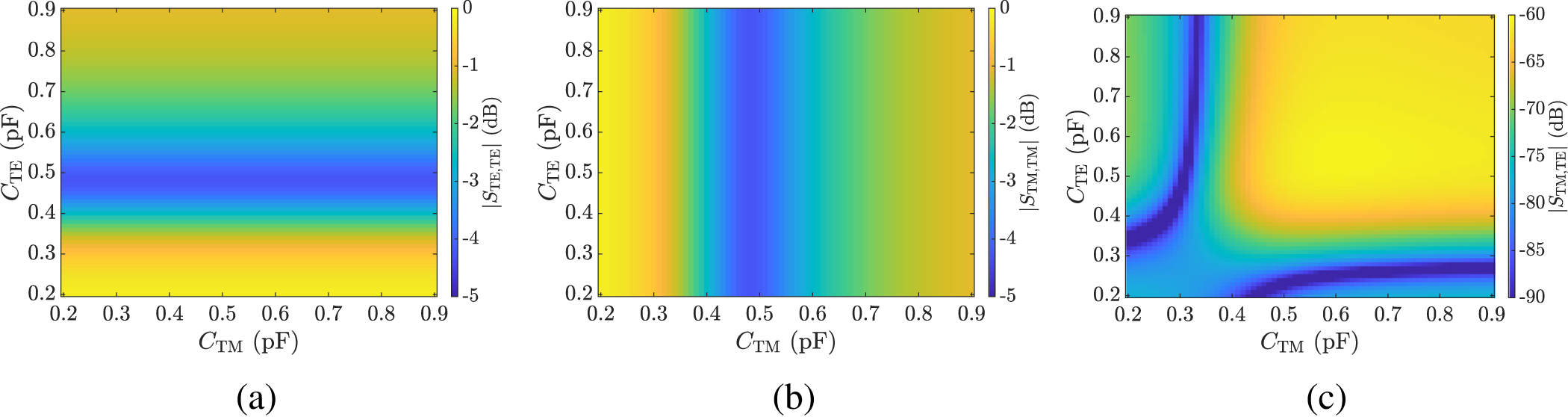
Figure 3 Long description
The image contains three plots illustrating the reflection coefficients for different capacitance combinations of varactor diodes. Plot (a) shows the magnitude of the reflection coefficient for TE/TE polarization with the x-axis labeled C subscript TM in picofarads and the y-axis labeled C subscript TE in picofarads. The reflection coefficient magnitude ranges from negative 1 to negative 5 decibels. Plot (b) displays the reflection coefficient for TM/TM polarization, with the same axis labels and a magnitude range from negative 1 to negative 5 decibels. Plot (c) presents the reflection coefficient for TM/TE polarization, with the x-axis labeled C subscript TM in picofarads and the y-axis labeled C subscript TE in picofarads. The magnitude ranges from negative 65 to negative 85 decibels.
Phase of the unit cell’s reflection coefficient for various capacitance combinations of the vertical and horizontal varactor diodes at  $15\,\mathrm{GHz}$: (a) TE/TE and (b) TM/TM.
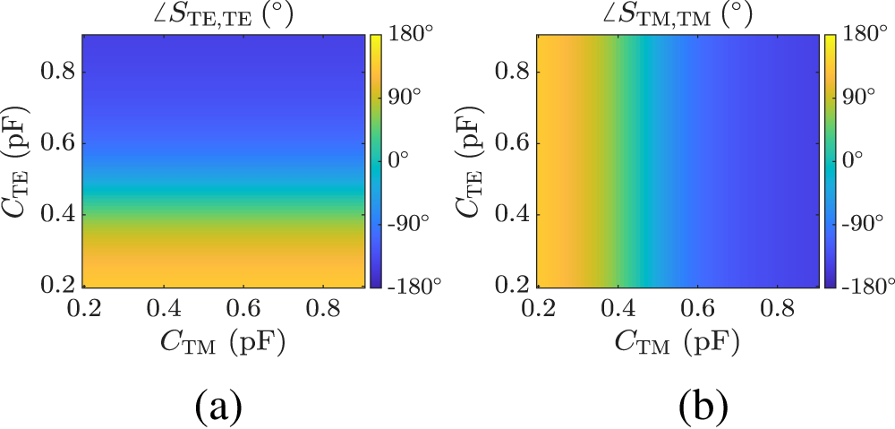
Figure 4 Long description
The image A shows a plot of the phase of the reflection coefficient for TE/TE polarization. The x-axis is labeled C subscript TM in picofarads, ranging from 0.2 to 0.8. The y-axis is labeled C subscript TE in picofarads, also ranging from 0.2 to 0.8. The color gradient represents phase values from negative 180 degrees to 180 degrees. The image B shows a plot of the phase of the reflection coefficient for TM/TM polarization. The axes are similarly labeled, with the same range for C subscript TM and C subscript TE. The color gradient is identical, representing phase values from negative 180 degrees to 180 degrees.
Reflection coefficient of the unit cell at  $15\,\mathrm{GHz}$: (a) magnitude and (b) phase.

Figure 5 Long description
The image contains two graphs labeled (a) and (b). Graph (a) displays the magnitude of the reflection coefficient, vertical axis labeled as absolute value of S subscript m n in decibels and horizontal axis labeled as C in picofarads. The curve shows a dip around 0.5 picofarads, with values ranging from 0 to negative 5 decibels. Graph (b) shows the phase of the reflection coefficient, vertical axis labeled as angle of S subscript m n in degrees and horizontal axis labeled as C in picofarads. The curve descends from 135 degrees to negative 180 degrees as capacitance increases from 0.2 to 0.9 picofarads. Both graphs include two data series, S subscript T E comma T E and S subscript T M comma T M, represented by different markers.
Figure 6(a) illustrates the magnitude of the surface current distribution on the radiating elements under TE-polarized broadside illumination. The bow-tie element, which integrates the varactor-diode function, serves as the main resonator and enables polarization-dependent tuning. It is observed that only the vertically polarized bow-tie element resonates, whereas the horizontally polarized one remains non-resonant. Under TM-polarized illumination, however, the horizontally oriented bow-tie element becomes resonant while the other does not, as shown in Fig. 6(b). This behavior enables independent control for each polarization. The square ring and patch elements, being dual-polarized, resonate under both polarization states. Similarly, Fig. 6(c) and (d) shows the magnitude of the surface current distribution on the radial stub and the transmission lines – which route the DC bias voltages to the varactor diodes through via holes – under TE- and TM-polarized illumination, respectively. It is observed that the RF power does not propagate through the radial stub, thereby protecting the DC bias network.
Surface current density magnitude at  $15\,\mathrm{GHz}$ for $C_\mathrm{TE} = C_\mathrm{TM} = {0.46}\,\mathrm{pF}$: radiation elements under (a) TE and (b) TM polarization, and radial stubs with transmission lines under (c) TE- and (d) TM-polarized broadside illumination.

Figure 6 Long description
The image A shows the surface current distribution on radiating elements under TE-polarized broadside illumination. It includes a bow-tie element resonating vertically, while the horizontally polarized element remains non-resonant. The square ring and patch elements resonate under both polarization states. The image B shows the surface current distribution under TM-polarized illumination, where the horizontally oriented bow-tie element becomes resonant, while the vertically polarized one does not. The square ring and patch elements resonate under both polarization states. The image C shows the surface current distribution on radial stubs and transmission lines under TE-polarized illumination. The radial stub does not propagate RF power, protecting the DC bias network. The image D shows the surface current distribution under TM-polarized illumination, with similar protection for the DC bias network. A color scale below the images indicates the magnitude from minimum to maximum.
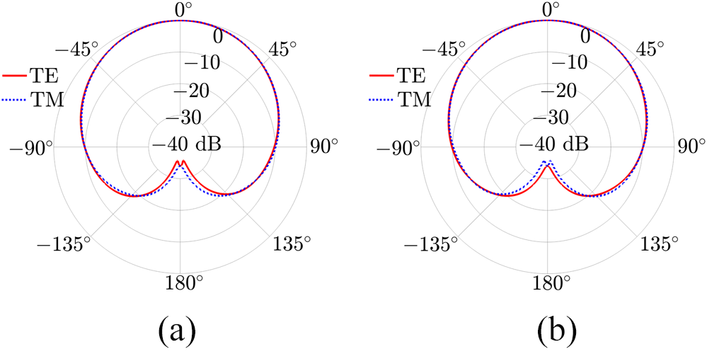
Figure 7 shows the normalized radiation pattern of the unit cell in the E-plane ( $xz$-plane, Fig. 7(a)) and H-plane ( $yz$-plane, Fig. 7(b)) under TE- and TM-polarized normal incidence at $15\,\mathrm{GHz}$. The results indicate that the unit cell exhibits a hemispherical radiation pattern. Because the unit-cell analysis employs periodic boundary conditions together with a Floquet port excitation, the array is assumed to be infinite; therefore, no edge diffraction occurs. Consequently, no back radiation is observed. Additionally, the half-power beamwidth of the unit cell is approximately $86.5^{\circ}$, providing a wide beam-steering capability.
Normalized radiation pattern of the unit cell at  $15\,\mathrm{GHz}$: (a) E-plane and (b) H-plane.

Figure 7 Long description
The image A shows a polar plot of the normalized radiation pattern for TE and TM modes at 15 GHz in the E-plane. The plot is circular with angles marked from 0 degrees to 360 degrees and radial lines indicating decibel levels from 0 dB to minus 40 dB. The TE mode is represented by a red line and the TM mode by a blue line. The image B shows a similar polar plot for the H-plane, with the same angular and radial markings. The TE and TM modes are again represented by red and blue lines, respectively.
RIS design and simulation
Figure 8(a) shows the array (RIS) configuration of the proposed unit cell. Since there are two varactor diodes per cell, we require two capacitances or phase distributions (one for TE, one for TM polarization) to steer the corresponding beam in the desired direction. Let us assume that there are  $M$ rows and $N$ columns in the RIS. The array factor of a planar antenna array is given as [Reference Balanis24]:
 \begin{equation}
\mathrm{AF}_p(\theta,\phi) = \sum_{m=1}^M \sum_{n=1}^N I_{mn,p} e^{j\mathbf{k} \cdot \mathbf{r}_{mn}} \text{,}
\end{equation}
\begin{equation}
\mathrm{AF}_p(\theta,\phi) = \sum_{m=1}^M \sum_{n=1}^N I_{mn,p} e^{j\mathbf{k} \cdot \mathbf{r}_{mn}} \text{,}
\end{equation}where  $I$ is the weight set of the array and $p=\{\mathrm{TE, TM}\}$ indicates the polarization state. In the case of RIS, the elements’ weights can be expressed as:
 \begin{equation}
I_{mn,p} = |I_{mn,p}| e^{j\psi_{mn,p}^\mathrm{ppd}} = |\Gamma_{mn,p}| e^{j\psi_{mn,p}^\mathrm{r}} e^{j\psi_{mn,p}^\mathrm{spd}} \text{,}
\end{equation}
\begin{equation}
I_{mn,p} = |I_{mn,p}| e^{j\psi_{mn,p}^\mathrm{ppd}} = |\Gamma_{mn,p}| e^{j\psi_{mn,p}^\mathrm{r}} e^{j\psi_{mn,p}^\mathrm{spd}} \text{,}
\end{equation}where  $\Gamma_{mn,p}=|\Gamma_{mn,p}| e^{j\psi_{mn,p}^\mathrm{r}}$ is the reflection coefficient of the associated cell, $\psi_{mn,p}^\mathrm{ppd}= -\mathbf{k}_{\mathrm{r},p} \cdot \mathbf{r}_{mn}$ is the required progressive phase delay between the cells to steer the beam in a desired direction (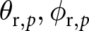 $\theta_{\mathrm{r},p}, \phi_{\mathrm{r},p}$), and $\psi_{mn,p}^\mathrm{spd}= -\mathbf{k}_{\mathrm{i},p} \cdot \mathbf{r}_{mn}$ is the spatial phase delay created by the incident wave (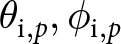 $\theta_{\mathrm{i},p}, \phi_{\mathrm{i},p}$) due to the different positions of the cells. The only unknown is the reflection phase of each element. Thus, it can be found as:
 \begin{equation}
\psi_{mn,p}^\mathrm{r} = \psi_{mn,p}^\mathrm{ppd} - \psi_{mn,p}^\mathrm{spd} \text{.}
\end{equation}
\begin{equation}
\psi_{mn,p}^\mathrm{r} = \psi_{mn,p}^\mathrm{ppd} - \psi_{mn,p}^\mathrm{spd} \text{.}
\end{equation}The progressive and spatial phase delays are
 \begin{equation}
\psi_{mn,p}^\mathrm{ppd} = -k(x_{mn}\sin\theta_{\mathrm{r},p}\cos\phi_{\mathrm{r},p} + y_{mn}\sin\theta_{\mathrm{r},p}\sin\phi_{\mathrm{r},p}) \text{,}
\end{equation}
\begin{equation}
\psi_{mn,p}^\mathrm{ppd} = -k(x_{mn}\sin\theta_{\mathrm{r},p}\cos\phi_{\mathrm{r},p} + y_{mn}\sin\theta_{\mathrm{r},p}\sin\phi_{\mathrm{r},p}) \text{,}
\end{equation} \begin{equation}
\psi_{mn,p}^\mathrm{spd} = k(x_{mn}\sin\theta_{\mathrm{i},p}\cos\phi_{\mathrm{i},p} + y_{mn}\sin\theta_{\mathrm{i},p}\sin\phi_{\mathrm{i},p}) \text{,}
\end{equation}
\begin{equation}
\psi_{mn,p}^\mathrm{spd} = k(x_{mn}\sin\theta_{\mathrm{i},p}\cos\phi_{\mathrm{i},p} + y_{mn}\sin\theta_{\mathrm{i},p}\sin\phi_{\mathrm{i},p}) \text{,}
\end{equation} $k$ is the wavenumber in air, and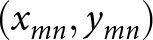 $(x_{mn}, y_{mn})$ are the Cartesian coordinates of the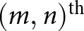 $(m,n)^\text{th}$ cell on the RIS surface plane.
RIS (a) topology and (b) view of  $16\times16$ panel.

Figure 8 Long description
The image A shows the RIS configuration of the proposed unit cell with varactor diodes labeled as C subscript TE and C subscript TM. The layout includes a grid of white dots forming a diagonal line across the square. The image B shows a 3D view of the panel with an incident wave and a reflected wave labeled. The panel is depicted as a grid with axes marked and the waves are shown with arrows indicating their direction.
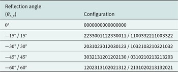
As an example, the proposed dual-polarized unit cell was used to construct a  $16\times16$ RIS panel ( $M=N=16$). The RIS was illuminated by an incident plane wave from the broadside (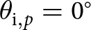 $\theta_{\mathrm{i},p}=0^\circ$,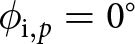 $\phi_{\mathrm{i},p}=0^\circ$), as shown in Fig. 8(b). The reflection angles of both polarizations were assumed to be identical (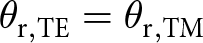 $\theta_{\mathrm{r,TE}}=\theta_{\mathrm{r,TM}}$) and were swept from $-60^{\circ}$ to $60^{\circ}$ in $15^{\circ}$ increments. The corresponding phase distributions were obtained from (3) and (4). The resulting phase delays were continuous. Due to the continuous tuning capability of the varactor diodes, these values could be used within the available phase range of $279^{\circ}$ at $15\,\mathrm{GHz}$. However, a 2-bit phase resolution was employed for simplicity in simulation. Four capacitance states were selected from Fig. 5(b) as #[0, 1, 2, 3] = [0.74, 0.485, 0.396, 0.2] pF, providing four distinct phase states [ $-135^{\circ}$, $-45^{\circ}$, $45^{\circ}$, $135^{\circ}$], respectively.
Figure 9 shows the simulated radar cross section (RCS) of the RIS for the considered scenarios. The colors in the plots represent different reflection angles; solid lines indicate the RCS under TE-polarized illumination, while dotted lines represent the RCS under TM-polarized incidence. Figure 9(a) illustrates the co-polarized RCS components for both TE and TM polarization, with the radiation pattern of the unit cell included as a dashed line to highlight the tapering effect of the element pattern on the array factor. This curve does not represent the peak RCS level; instead, it serves as an envelope that indicates the influence of the element pattern on the RIS response across different reflection angles. The unit-cell radiation pattern is obtained from the simulations and was previously presented in Fig. 7. On the other hand, Fig. 9(b) shows the cross-polarized components. The results indicate that the RIS provides accurate wide-angle beam-steering capability within  $\pm60^\circ$, with maximum beam-pointing errors of $1.7^{\circ}$ and $1.2^{\circ}$ for TE and TM polarization, respectively. The RCS values for TE- and TM-polarized illumination are nearly identical within the $\pm45^\circ$ beam-steering range, where the beam-pointing error remains below $1^{\circ}$. The peak RCS points follow the radiation pattern of the unit cell except at $\pm15^\circ$, where larger 2-bit quantization errors result in stronger side-lobes. Moreover, the peak RCS under TM polarization is approximately $1.2\,\mathrm{dB}$ higher than that under TE polarization at $\pm60^\circ$, which may be attributed to the non-symmetric geometry of the RIS panel. Examining the cross-polarized components, the cross-polarization discrimination (XPD) exceeds $45\,\mathrm{dB}$ at $15\,\mathrm{GHz}$. The capacitance distribution of the diodes for each scenario is provided in Table 2.
Simulated RCS of the RIS for various reflection angles under broadside plane-wave incidence at  $15\,\mathrm{GHz}$: (a) co-polarized RCS components, with the unit cell radiation pattern shown as a dashed line, and (b) cross-polarized RCS components.

Figure 9 Long description
The image A shows a graph of radar cross section (RCS) in decibel square meter versus elevation angle in degrees. The graph includes solid lines for TE-polarized illumination and dotted lines for TM-polarized incidence. Various curves represent different reflection angles ranging from negative 60 degrees to positive 60 degrees. The dashed line indicates the unit cell radiation pattern. The RCS values range from negative 10 to 15 decibel square meter. The image B shows a graph of radar cross section (RCS) in decibel square meter versus elevation angle in degrees. Similar to image A, it includes solid lines for TE-polarized illumination and dotted lines for TM-polarized incidence. Various curves represent different reflection angles ranging from negative 60 degrees to positive 60 degrees. The RCS values range from negative 75 to 15 decibel square meter.
RIS capacitance distributions for various reflection angles under broadside plane-wave illumination at  $15\,\mathrm{GHz}$
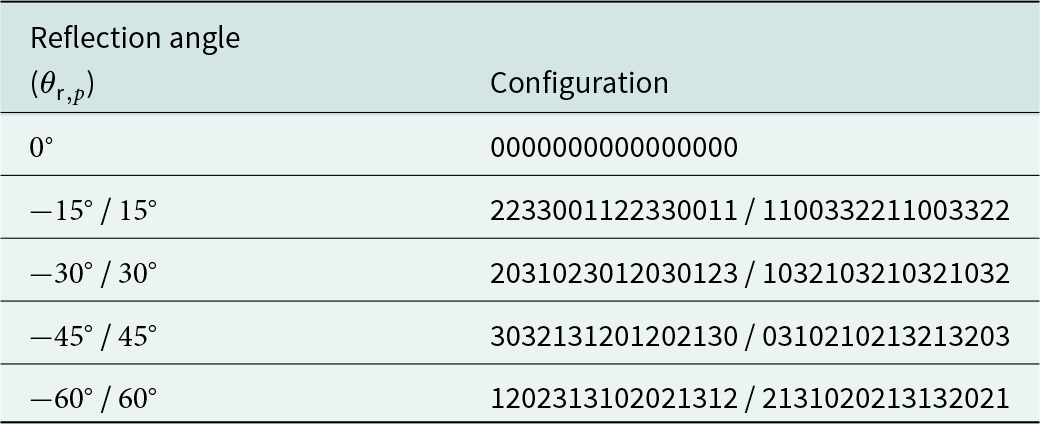
Table 2 Long description
The table presents capacitance configurations for different reflection angles under broadside plane-wave illumination at fifteen gigahertz. At zero degrees, the configuration is uniform with all zeros. For negative fifteen and positive fifteen degrees, the configurations show a repeating pattern of numbers, indicating a symmetrical distribution. As the reflection angle increases to negative thirty and positive thirty degrees, the configurations become more complex, with varied sequences of numbers. Negative forty-five and positive forty-five degrees show further complexity, with distinct sequences that differ from other angles. The configurations for negative sixty and positive sixty degrees also exhibit unique patterns, suggesting a relationship between angle and capacitance distribution. These variations highlight how reflection angles influence capacitance configurations, which may be crucial for optimizing performance in related applications.
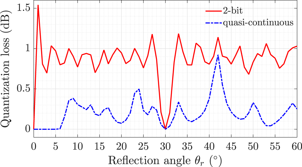
Figure 10 illustrates the RIS array-factor (1) performance for different phase-resolution techniques. It is observed that, with 2-bit phase resolution, the quantization loss – defined as the difference in dB between the peak values of the continuous and quantized array factors – is approximately  $1\,\mathrm{dB}$. When a quasi-continuous phase distribution is employed – i.e., continuous within the achievable phase-shift range and mapped to the nearest boundary outside this range – the quantization loss is reduced to below $0.5\,\mathrm{dB}$. This technique is advantageous because the capacitance of varactor diodes can be continuously controlled via the applied reverse-bias voltage. Furthermore, at $30^{\circ}$ (corresponding to a $90^{\circ}$ phase shift between adjacent columns), the quantized and continuous phase distributions coincide, resulting in no quantization loss. Since there is no quantization error at $0^{\circ}$ and $\pm 30^{\circ}$, the RCS at $\pm 15^{\circ}$ is lower than the RCS values at those angles.
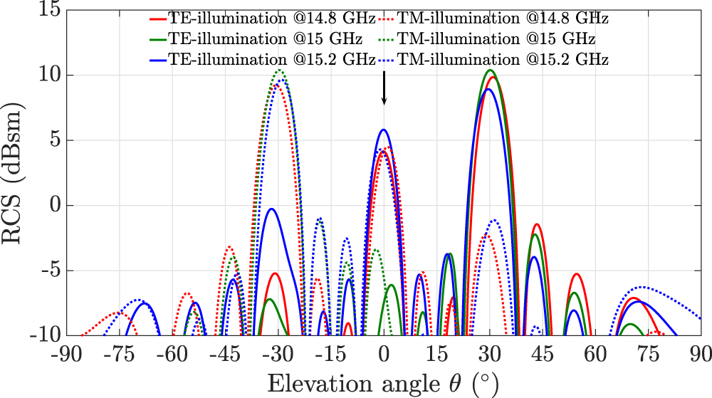
To illustrate the independent control of both polarizations and the beam-steering performance within the 2-bit phase resolution bandwidth (i.e., 14.8– $15.2\,\mathrm{GHz}$), vertically placed varactor diodes were configured for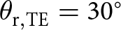 $\theta_{\mathrm{r,TE}}=30^\circ$, while horizontally placed varactor diodes were configured for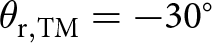 $\theta_{\mathrm{r,TM}}=-30^\circ$, with the angle of incidence set to broadside. As shown in Fig. 11, the reflected beam from the RIS is directed toward $-30^{\circ}$ under a TM-polarized incident plane wave and toward $30^{\circ}$ under a TE-polarized incident wave at $14.8$, $15$, and $15.2\,\mathrm{GHz}$. The beam-pointing error remains below $1^{\circ}$; however, the specular reflection increases because the phase distribution on the RIS surface is not ideally matched, resulting in reduced beam-steering performance, similar to a beam-squint effect.
RIS array factor performance under normal incidence with different phase resolution techniques.

Figure 10 Long description
A line graph comparing quantization loss in decibels for two phase resolution techniques: 2-bit and quasi-continuous. The x-axis represents the reflection angle theta subscript r in degrees, ranging from 0 to 60. The y-axis shows quantization loss in decibels, ranging from 0 to 1.5. The red solid line represents the 2-bit resolution, showing higher quantization loss with peaks around 1.5 decibels at lower angles and fluctuating around 1 decibel at higher angles. The blue dashed line represents the quasi-continuous resolution, showing lower quantization loss, with peaks below 1 decibel and a notable dip at 30 degrees where the loss approaches zero. The graph illustrates the performance differences between the two techniques across the angle range.
Simulated RCS of the RIS under broadside plane-wave illumination with 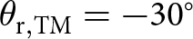 $\theta_{\mathrm{r,TM}}=-30^\circ$ and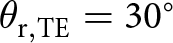 $\theta_{\mathrm{r,TE}}=30^\circ$ at different frequency points.

Figure 11 Long description
A graph showing the radar cross-section (RCS) in decibel square meters plotted against the elevation angle in degrees. The graph includes six curves representing TE and TM illumination at three different frequencies: 14.8 GHz, 15 GHz and 15.2 GHz. The TE illumination curves are shown with solid lines, while TM illumination curves are shown with dotted lines. The elevation angle ranges from negative 90 degrees to positive 90 degrees and the RCS values range from negative 10 to positive 15 decibel square meters. Peaks are visible at various angles, with notable peaks around negative 30 degrees for all frequencies.
Figure 12(a) shows the RCS of the RIS under oblique incidence. The angles of incidence for the TE- and TM-polarized plane waves were set to 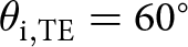 $\theta_{\mathrm{i,TE}}=60^\circ$ and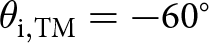 $\theta_{\mathrm{i,TM}}=-60^\circ$, respectively, while the reflected beams were configured for $\theta_{\mathrm{r,TE}}=\theta_{\mathrm{r,TM}}=0^\circ$. Due to the angular reciprocity of the RIS, the same capacitance configurations listed in Table 2 could be used. It is observed that under wide oblique incidence, beam steering remains highly accurate, with an error below $0.5^{\circ}$. The difference between the anomalous reflection (steered beam) and the specular reflection under TE-polarized illumination is approximately $10.8\,\mathrm{dB}$, whereas it is reduced under TM-polarized illumination, despite the higher peak RCS. This behavior may be attributed to the fact that the unit cell responds differently under wide oblique incidence for the two polarizations. The capacitance states do not maintain the required $90^{\circ}$ phase spacing under wide oblique incidence, leading to increased quantization error. To demonstrate the angular robustness of the proposed RIS, the array was evaluated under different incidence and reflection scenarios. Figure 12(b) shows the RCS in the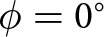 $\phi=0^\circ$ plane when the RIS is configured for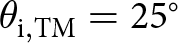 $\theta_{\mathrm{i,TM}}=25^\circ$,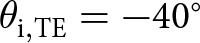 $\theta_{\mathrm{i,TE}}=-40^\circ$,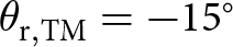 $\theta_{\mathrm{r,TM}}=-15^\circ$, and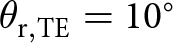 $\theta_{\mathrm{r,TE}}=10^\circ$. Similarly, Fig. 12(c) presents the 3D RCS when beam steering is applied in both planes, with $(\theta_{\mathrm{i},p},\phi_{\mathrm{i},p}) = (-20^\circ, 0^\circ)$ and $(\theta_{\mathrm{r},p},\phi_{\mathrm{r},p}) = (35^\circ, 45^\circ)$, represented in the $u$–
$u$– $v$ domain, where $u \triangleq \sin\theta\cos\phi$ and $v \triangleq \sin\theta\sin\phi$. It is observed that the RIS successfully steers the beam in both planes with low beam-pointing error, even with 2-bit phase resolution.
Simulated RCS of the RIS at  $15\,\mathrm{GHz}$ under oblique incidence. (a) Incident TM: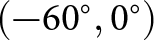 $(-60^\circ,0^\circ)$, TE: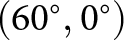 $(60^\circ,0^\circ)$, reflection: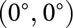 $(0^\circ,0^\circ)$. (b) TM: incidence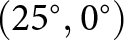 $(25^\circ,0^\circ)$, reflection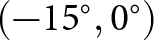 $(-15^\circ,0^\circ)$; TE: incidence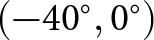 $(-40^\circ,0^\circ)$, reflection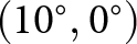 $(10^\circ,0^\circ)$. (c) TM, TE: incidence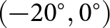 $(-20^\circ,0^\circ)$, reflection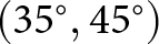 $(35^\circ,45^\circ)$.

Figure 12 Long description
The image consists of three graphs labeled (a), (b) and (c). Graph (a) shows the radar cross-section (RCS) in decibel square meter versus elevation angle in degrees for TE and TM polarizations. The TE curve is solid and the TM curve is dotted. Incidence and reflection points are marked with arrows. Graph (b) similarly displays RCS versus elevation angle for TE and TM polarizations, with incidence and reflection points indicated. Graph (c) presents two circular plots for TE and TM-polarized illumination, showing RCS in the u-v domain. The TE plot is on the left and the TM plot is on the right. Each plot includes a color scale indicating RCS values, with incident and reflected waves marked by symbols.
Experimental validation of the unit cell
There are several methods to validate the characteristics of a unit cell. One common approach is to use a waveguide simulator [Reference Abbasi and Ismail25], in which the unit cell is inserted into a waveguide to measure the phase and magnitude of the reflected waves. However, this technique does not account for the coupling between adjacent cells. In other words, the periodic boundary conditions typically employed in full-wave simulations are not replicated in this measurement setup. As a result, mutual coupling effects between unit cells are not considered. Two unit cells may also be inserted into a waveguide to partially account for mutual coupling, although only the coupling from one neighboring side is captured [Reference Scheder, Fleischmann, Gröschel and Vossiek10]. Another approach is to measure the macroscopic response of the entire surface, which can be used to validate the unit cell’s characteristics [Reference Araghi, Khalily, Safaei, Bagheri, Singh, Wang and Tafazolli26]. To incorporate coupling from all surrounding elements, the unit cell can be characterized by placing it at the center of a  $3\times3$ array [Reference Neuder, Liu, Dzieia, Wang and Jiménez-Sáez6]. The $3\times3$ array constitutes the minimum configuration that approximates the mutual coupling in periodic boundary conditions. In this setup, the central element is coupled to all surrounding elements, whereas the edge elements are only partially coupled. Nevertheless, this configuration provides a reasonable representation of the electromagnetic environment in simulation using a minimum number of elements. Figure 13(a) shows the fabricated $3\times3$ prototype of the proposed unit cell. To bias the varactor diodes, DC pin headers were placed on the backside of the prototype, and these pins were connected to the corresponding via holes through DC traces, as illustrated in Fig. 13(b). To further minimize RF leakage, thick film 10 k $\Omega$ resistors were included in the biasing network. Figure 13(c) shows the schematic of the bias circuit. The anodes of all varactor diodes are connected to ground, while their cathodes are connected to the input-voltage pins through resistors. Since all varactor diodes are reverse-biased, no DC current flows through the resistors, and therefore no DC voltage drop occurs across them.
Fabricated  $3\times3$ prototype: (a) top view with varactor diode IDs, (b) bottom view, and (c) schematic of the biasing circuit.

Figure 13 Long description
The first image (a) shows the top view of a prototype with labeled varactor diodes arranged in a grid pattern. The labels include TE left parenthesis 1 comma 1 right parenthesis, TE left parenthesis 1 comma 2 right parenthesis, TM left parenthesis 1 comma 1 right parenthesis and TM left parenthesis 2 comma 1 right parenthesis. The varactor diodes are positioned within a three by three grid. The second image (b) displays the bottom view of the prototype, featuring pin headers and a 10 kilo ohm resistor. The pin headers are aligned along one edge and the resistor is circled for emphasis. The board is labeled as 3 by 3 RIS Prototype v1.0 2025. The third image (c) illustrates the schematic of the biasing circuit. It includes pin headers connected to resistors and varactor diodes, with the anodes of the diodes connected to ground. The cathodes are connected to the input-voltage pins through resistors. The schematic shows connections for TE and TM labeled diodes, arranged in a sequence with ground connections at the bottom.
Monostatic measurement
Figure 14(a) shows the monostatic measurement setup used for the fabricated prototype. An R&S®HMP2030 power supply (PS) was used to bias the varactor diodes. The first channel of the PS was assigned to the vertically oriented varactor diodes, while the second channel was assigned to the horizontally oriented ones. Half of the top DC bias pins on the prototype were connected to the first channel, and the remaining pins were connected to the second channel. The bottom pins were connected to ground. An MVG QH2000 open-boundary quad-ridge horn antenna was used as the measurement antenna, and its ports were connected to an R&S®ZVA24 vector network analyzer (VNA). The separation between the measurement antenna and the prototype was set to  ${35}\,\mathrm{cm}$. To enable remote control, a controller PC was connected to both the VNA and the PS through an Ethernet switch. Absorber walls were placed behind the prototype and in front of the PS and VNA to reduce reflections from the equipment and the surrounding environment. The measurement environment is shown in Fig. 14(b).
Monostatic measurement setup: (a) block diagram and (b) photograph of the environment.

Figure 14 Long description
The image A shows a block diagram of a monostatic measurement setup. It includes a vector network analyzer connected to a measurement antenna, which is positioned 35 centimeters from a 3 by 3 reconfigurable intelligent surface. Absorber walls are placed around the setup to minimize reflections. A direct current power supply is connected to the reconfigurable intelligent surface, with channels labeled Ch1, Ch2 and Ch3. An Ethernet switch connects the vector network analyzer and the power supply to a personal computer for remote control. The image B shows a photograph of the actual setup environment. It features three panels with absorber material arranged around a central measurement device. The room has large windows and various equipment, including a tripod supporting the measurement device, positioned between the absorber panels.
The VNA was calibrated using an R&S®ZV-Z52 electronic calibration kit to compensate for systematic errors introduced by the cables and connectors. The reflection coefficients of the measurement antenna (i.e., 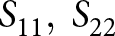 $S_{11}, \: S_{22}$) were then measured under different reverse-bias voltages applied to the varactors, ranging from 0 to 10 V. Measurements taken with the prototype were divided by the antenna-only measurement (without the prototype) to obtain the reflection magnitude associated with the RIS. Although absorber walls were used, the measurement environment still introduced multipath reflections; therefore, time-gating was applied to the collected data.
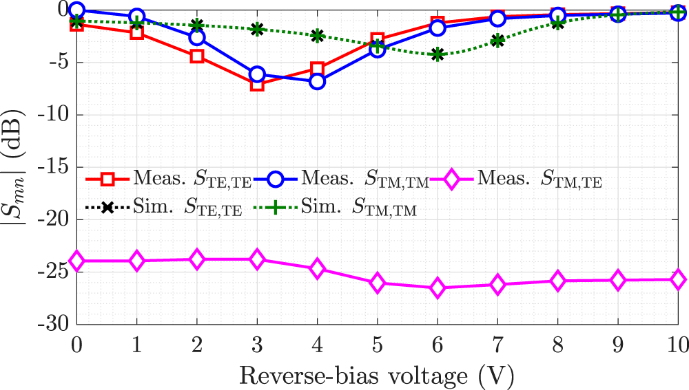
Figure 15 shows the measured normalized reflection coefficient magnitude at  $15\,\mathrm{GHz}$ for various reverse-bias voltages. Note that all varactor diodes were biased with the same voltage. The resulting reflection-magnitude trend resembles that obtained in the simulation, with a slight shift. This shift is most likely attributed to fabrication tolerances, which can cause a frequency shift in the response. The difference observed between the two polarization states may be attributed to the nonidentical responses of the two antenna ports. The maximum reflection loss of the prototype is approximately $7\,\mathrm{dB}$, which is slightly higher than that observed in the simulations. This discrepancy may be attributed to the internal resistance of the varactor diodes, which might be slightly higher than the values used in the simulation model. Furthermore, the elements in the $3\times3$ array do not exhibit identical electrical behavior. While the central element is affected by mutual coupling from all surrounding elements, the edge elements experience reduced coupling. Consequently, even when identical bias voltages are applied, the response of each unit cell may differ. This non-uniformity can disturb the intended phase distribution across the surface and distort the reflected beam. As a result, a portion of the reflected power may be redirected into side lobes, appearing as a loss at the receiver, although it does not correspond to true absorptive loss. The reflection loss can be reduced by increasing the substrate thickness, but this comes at the expense of a narrower phase-shift range.
Monostatic measurement of the reflection magnitude for various reverse-bias voltages at  $15\,\mathrm{GHz}$.

Figure 15 Long description
A line graph showing the reflection magnitude in decibels on the y-axis and reverse-bias voltage in volts on the x-axis, ranging from 0 to 10 volts. The graph includes four curves: a red line with square markers for measured S subscript TE comma TE, a blue line with circle markers for measured S subscript TM comma TM, a magenta line with diamond markers for measured S subscript TM comma TE and a green dotted line with plus markers for simulated S subscript TM comma TM. Additionally, a black dotted line with cross markers represents simulated S subscript TE comma TE. The measured S subscript TE comma TE and S subscript TM comma TM curves show a trend of decreasing reflection magnitude with increasing voltage, while the measured S subscript TM comma TE remains relatively constant. The simulated curves show a similar trend with slight variations. The legend identifies each curve with its corresponding mode and measurement type.
There is a certain deterioration in the measured XPI relative to the simulated one. This discrepancy may arise from several factors. First, the excitation used in simulations is an ideal plane-wave source, whereas in measurements, the antenna cannot perfectly generate a linearly polarized plane wave over the prototype surface. Moreover, a dual-polarized antenna is employed as the measurement antenna, and its port-to-port isolation is not perfect, which can further degrade the XPI. In addition, the prototype is very small, making precise alignment between the antenna and the unit cell challenging. Not only must the direct alignment be accurate, but the dual-polarized measurement antenna must also be oriented exactly at  $90^{\circ}$. Even a slight rotation of the measurement antenna or a small misalignment between the antenna and the prototype may increase polarization leakage. Although time-gating was applied, residual reflections from the surrounding environment may still contribute to deterioration – for example, reflections from the tripod positioned at the same distance as the prototype – since the measurement environment is not fully anechoic. Finally, due to the small size of the varactor diodes, they cannot be positioned with perfect accuracy during soldering, leading to placement errors. These placement errors and potential damage to varactor diodes may result in non-ideal biasing. Despite these factors, the measured XPI values, although lower than the simulated ones, remain around $24\,\mathrm{dB}$.
Bistatic measurement
Although variations in the reflection magnitude of the prototype were observed for different bias voltages, corresponding variations in the phase response could not be clearly identified in the monostatic measurements. This may be because the phase response of the antenna port dominates the overall reflection phase, masking the contribution from the prototype, since the prototype is very small and the backscatter is very weak. Therefore, a bistatic measurement setup was employed, as shown in Fig. 16(a), to estimate the reflection phase of the prototype more accurately. Two MVG QH2000 open-boundary quad-ridge horn antennas were used as the transmit (Tx) and receive (Rx) antennas, each oriented toward the prototype at  $10^{\circ}$. The distance between the antennas and the prototype was set to ${185}\,\mathrm{cm}$ to reduce direct interaction between the Tx and Rx antennas. All other measurement equipment remained the same, and the bistatic measurement environment is presented in Fig. 16(b).
Bistatic measurement setup: (a) block diagram and (b) photograph of the environment.

Figure 16 Long description
The image A shows a block diagram of a bistatic measurement setup. It includes a 3 by 3 RIS positioned at a 10-degree angle between two antennas labeled RX and TX, each 185 cm from the RIS. The antennas are connected to a vector network analyzer and a PC via an Ethernet switch. A DC power supply with channels Ch1, Ch2 and Ch3 is also depicted. Absorber walls are shown at the top. The image B shows a photograph of the measurement environment. It features two antennas on tripods facing a panel with absorber material. The setup is in a room with windows and additional equipment visible in the background.
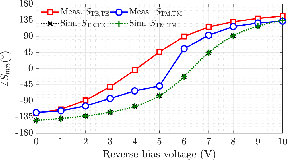
In this configuration, the transmission coefficient was measured using the VNA for different reverse-bias voltages applied to the varactors, ranging from 0 to 10 V. Due to the non-anechoic environment, time-gating was applied to all measurements. The prototype was then replaced with a metal plate of similar size, and the measurement was repeated with the same time-gating parameters. As a post-processing calibration step, the measurements obtained with the prototype were divided by the corresponding metal-plate measurements. Figure 17 shows the measured reflection coefficient phase at  $15\,\mathrm{GHz}$ for various reverse-bias voltages. It is observed that the maximum phase shift is approximately $270^{\circ}$, and the curves are similar to those obtained from simulations, exhibiting a shift comparable to that observed in the monostatic measurements.
Bistatic measurement of the reflection phase for various reverse-bias voltages at  $15\,\mathrm{GHz}$.

Figure 17 Long description
A line graph showing the reflection phase L S subscript mn in degrees on the y-axis versus reverse-bias voltage in volts on the x-axis, ranging from 0 to 10 volts. The graph includes four curves: measured S subscript TE comma TE represented by red squares, measured S subscript TM comma TM represented by blue circles, simulated S subscript TE comma TE represented by black crosses and simulated S subscript TM comma TM represented by green asterisks. The measured S subscript TE comma TE curve starts at approximately negative 135 degrees and rises steadily to about 135 degrees at 10 volts. The measured S subscript TM comma TM curve starts at approximately negative 135 degrees and rises to about 90 degrees at 10 volts. The simulated S subscript TE comma TE curve starts at approximately negative 135 degrees and rises to about 45 degrees at 10 volts. The simulated S subscript TM comma TM curve starts at approximately negative 135 degrees and rises to about 0 degrees at 10 volts.
Due to its small size and the relatively large distance between the antennas and the prototype, the magnitude of the reflected wave from the RIS is very weak, and the variations in magnitude are not as pronounced as in the monostatic case. This indicates that, for small surfaces, bistatic setups are more suitable for phase measurements, whereas monostatic setups are more appropriate for magnitude measurements. For larger surfaces, however, both measurement techniques are expected to provide similar results.
The total efficiency of the RIS can be defined as the ratio between the measured and ideal values for bistatic scenarios – without accounting for measurement tolerances [Reference Ataloglou and Eleftheriades27]:
 \begin{equation}
\eta_\mathrm{tot} := \frac{\left|S_{21}^{\mathrm{meas}}(\theta_\mathrm{r})\right|^2}{\left|S_{21}^{\mathrm{ideal}}(\theta_\mathrm{i}, \theta_\mathrm{r})\right|^2}
\text{.}
\end{equation}
\begin{equation}
\eta_\mathrm{tot} := \frac{\left|S_{21}^{\mathrm{meas}}(\theta_\mathrm{r})\right|^2}{\left|S_{21}^{\mathrm{ideal}}(\theta_\mathrm{i}, \theta_\mathrm{r})\right|^2}
\text{.}
\end{equation}The ideal forward transmission (S-parameter) coefficient can be found from the bistatic radar equation:
 \begin{equation}
\left|S_{21}^{\mathrm{ideal}}(\theta_\mathrm{i}, \theta_\mathrm{r})\right|^2 = \sigma(\theta_\mathrm{i}, \theta_\mathrm{r})\frac{G^2}{4\pi}\left(\frac{\lambda}{4\pi R^2} \right)^2,
\end{equation}
\begin{equation}
\left|S_{21}^{\mathrm{ideal}}(\theta_\mathrm{i}, \theta_\mathrm{r})\right|^2 = \sigma(\theta_\mathrm{i}, \theta_\mathrm{r})\frac{G^2}{4\pi}\left(\frac{\lambda}{4\pi R^2} \right)^2,
\end{equation}assuming that both the Tx and Rx antennas have the same realized gain ( $G$) and are located at the same distance ( $R$) from the RIS, the RCS of the RIS in an ideal case is given by [Reference Trichopoulos, Theofanopoulos, Kashyap, Shekhawat, Modi, Osman, Kumar, Sengar, Chang and Alkhateeb28]
 \begin{equation}
\sigma(\theta_\mathrm{i}, \theta_\mathrm{r}) = 4\pi\frac{(L_xL_y)^2}{\lambda^2}\cos\theta_\mathrm{i}\cos\theta_\mathrm{r}
\text{,}
\end{equation}
\begin{equation}
\sigma(\theta_\mathrm{i}, \theta_\mathrm{r}) = 4\pi\frac{(L_xL_y)^2}{\lambda^2}\cos\theta_\mathrm{i}\cos\theta_\mathrm{r}
\text{,}
\end{equation}where ( $L_x,L_y$) is the size of the RIS.
When all the diodes are biased with the same voltages, only the specular reflection occurs and 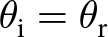 $\theta_\mathrm{i}=\theta_\mathrm{r}$. From the bistatic unit-cell measurements, the total efficiency of the RIS prototype was found to be approximately 42% under a reverse zero-voltage bias.
To validate the unit cell’s radiation performance, a bistatic radiation pattern measurement setup was implemented. Figure 18(a) shows the diagram of the measurement setup. The  $3\times3$ RIS prototype was mounted at the center of a rotating stage (rotary gimbal), and the TX antenna was positioned ${50}\,\mathrm{cm}$ away from the prototype, pointing towards it, using a carbon pipe. Therefore, the prototype and Tx antenna rotate together, and the angle of incidence is always from boresight. The Rx antenna was placed ${125}\,\mathrm{cm}$ away from the prototype, and its position was fixed. All the diodes were biased at 0 V, and the measurements were performed using the VNA. Measurements were recorded at each angular position of the gimbal, ranging from $-90^{\circ}$ to $90^{\circ}$ with $1^{\circ}$ increments. Figure 18(b) shows the measurement environment.
Radiation pattern bistatic measurement setup: (a) block diagram and (b) photograph of the environment.

Figure 18 Long description
The first image is a block diagram illustrating a bistatic radiation pattern measurement setup. It includes a DC power supply with three channels, a three by three RIS prototype mounted on a rotating stage and absorber walls. The TX antenna is positioned 50 cm away from the prototype using a carbon rod and the RX antenna is placed 125 cm away. The setup is connected to a vector network analyzer and a PC via an Ethernet switch. The second image is a photograph of the measurement environment, showing the equipment setup with the RIS prototype on a table, surrounded by various electronic devices and cables. The environment includes large windows providing natural light.
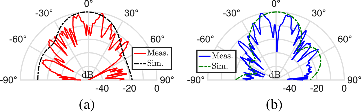
Figure 19 depicts the normalized radiation pattern of the prototype. Ideally, the unit-cell radiation pattern could be extracted using theoretical array-factor calculation. However, since not all cells behave identically due to mutual-coupling effects, a full-wave simulation of a  $3\times3$ array was performed and is provided alongside the measurements for comparison. Due to the non-anechoic measurement environment, fluctuations are observed in the measured pattern – despite the utilization of the time-gating technique in post-processing. Furthermore, a blind spot appears around $0^{\circ}$. This is caused by the shadowing/blockage effect of the Tx antenna, which is positioned in front of the Rx antenna. In addition, as the angle approaches $90^{\circ}$, the gimbal arm begins to block the radiation from the prototype. Despite these effects, the overall envelope of the measured data shows good agreement with the simulation results.
Measured and simulated normalized radiation pattern of 3  $\times$ 3 RIS prototype: under (a) TE and (b) TM polarized normal incidence.

Figure 19 Long description
The image consists of two polar plots. The first plot (a) shows the measured and simulated radiation patterns for TE polarized normal incidence. The measured pattern is represented by a solid line, while the simulated pattern is shown with a dashed line. The second plot (b) displays the measured and simulated radiation patterns for TM polarized normal incidence. Here, the measured pattern is depicted with a solid line and the simulated pattern with a dashed line. Both plots have angles marked from negative 90 degrees to positive 90 degrees, with the radial axis labeled in decibels (dB).
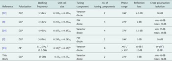
Finally, Table 3 provides a comparison between the proposed unit cell and previously reported RIS and reflectarray unit cells. The results show that the proposed unit cell achieves one of the highest XPI levels while providing a phase-shift range of  $270^{\circ}$ and simultaneously minimizing the number of required tuning components, thus reducing the overall cost of an RIS panel.
Comparison of the proposed unit cell with previously reported RIS and reflectarray unit cells
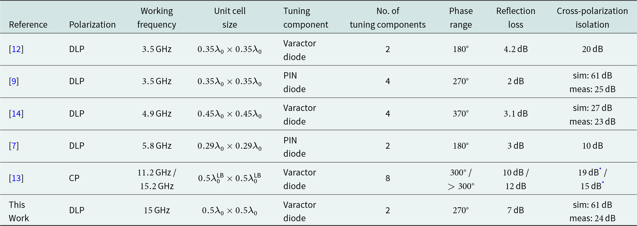
Table 3 Long description
The table compares unit cells based on polarization, frequency, size, tuning components, and performance metrics like phase range, reflection loss, and cross-polarization isolation. The proposed unit cell operates at 15 GHz with dual-linear polarization, using a varactor diode for tuning, and achieves a reflection loss of 7 dB and a measured cross-polarization isolation of 24 dB. In comparison, other designs operate at frequencies ranging from 3.5 GHz to 15.2 GHz, with varying unit cell sizes and tuning components like PIN diodes. Notably, the design from reference [9] achieves the highest simulated cross-polarization isolation of 61 dB at 3.5 GHz. The proposed design's performance is competitive, especially in terms of cross-polarization isolation, despite operating at a higher frequency.
Notes: All results presented above are measurement results unless stated otherwise. DLP: dual-linear polarized. CP: circularly-polarized. LB: lower-band.
(*) The given values are XPD: cross-polarization discrimination.
Conclusion
A dual-polarized RIS with high XPI operating within the upper mid-band, one of the key candidate spectra for 6G, has been presented. The topology and structure of the proposed unit cell have been discussed, and detailed analyses of both the unit cell and the  $16\times16$ RIS have been provided. The number of adjustable components has been minimized to only two varactor diodes for dual-polarized operation, resulting in lower cost, simpler structure, and improved robustness. Simulation results show that the unit cell achieves more than $270^{\circ}$ of phase-shift range with a maximum reflection loss of $4.5\,\mathrm{dB}$ and an XPI exceeding $61\,\mathrm{dB}$ within the 14.8– ${15.2}\,\mathrm{GHz}$ band. The $16\times16$ RIS achieves a wide beam-scanning capability of $\pm60^\circ$ with a maximum simulated beam-pointing error of only $1.7^{\circ}$. To validate the unit-cell characteristics, a $3\times3$ prototype was fabricated. Two different measurement techniques were evaluated to characterize such a small prototype in a non-anechoic environment. The measurement results show good agreement with simulations, providing a phase range of $270^{\circ}$, approximately $7\,\mathrm{dB}$ reflection loss, and an XPI of around $24\,\mathrm{dB}$. It is also observed that bistatic measurement setups are more suitable for phase characterization, whereas monostatic setups are more appropriate for magnitude measurements of small surfaces. Overall, the proposed unit cell shows good potential for future 6G applications, particularly in full-duplex and ISAC systems, owing to its high polarization isolation.
As future work, a  $16\times16$ RIS panel will be fabricated and tested to validate the array-level performance of the proposed RIS and will be deployed in a full-duplex or ISAC scenario for real-world demonstration.
Acknowledgements
The authors would like to thank the Federal Ministry of Research, Technology, and Space (BMFTR) for supporting the xG-RIC project as part of the research program Communication Systems “Souverän. Digital. Vernetzt” (grant number: 16KIS2429K), and for supporting the DE-TW-GLEMORIS project (grant number: 16ME1100), funded under the framework program for Research and Innovation “Microelectronics. Trustworthy and sustainable. For Germany and Europe” – a BMFTR/NSTC joint funding program: Research collaboration in microelectronics between Germany and Taiwan.
Competing interests
The author(s) declare none.

Mehmet Ahad Yurtoglu received his Bachelor’s degree in Electrical and Electronics Engineering from Gazi University, Türkiye, in 2021. In 2023, he received his Master of Science (M.Sc.) degree with cum laude in Telecommunication Engineering from Politecnico di Milano, Italy. Currently, he is a research associate at Fraunhofer HHI. He is interested in antennas, antenna arrays, microwave filters, filtering antennas, and reconfigurable intelligent surfaces.

Ramez Askar (IEEE SM) received his B.Eng. in 2008 from Homs (formerly AL-Baath) University, his M.Sc. in 2013 from Ilmenau University of Technology, and his Ph.D. (summa cum laude) in 2022 from Technische Universität Berlin. He is the deputy head of the mmWave Research group at Fraunhofer HHI. His research interests include full-duplex, self-interference channels and cancellation, transceiver hardware impairments, and sub-THz RF system design and propagation. He has published numerous peer-reviewed papers, journals, and patents – some of which are licensed – in his area of expertise. He received the Best Paper Award at IEICE SmartCom 2017 and the Best Demo awards at the 2024 IEEE 6G Summit in Dresden and the 2024 IEEE 6G Summit in Brooklyn.

Sven Wittig received B.Sc. and M.Sc. in electrical engineering from RWTH Aachen University in 2014 and 2016, respectively. Since 2017, he has been with the mmWave group at the Fraunhofer HHI. His main areas of interest are RF measurement systems and instrumentation, with a focus on wireless propagation channels and prototyping of broadband communication systems.

Mathis Schmieder received B.S. and M.S. in Electrical Engineering from Technische Universität Berlin in 2012 and 2017, respectively. Since then, he has been with the Fraunhofer HHI. He is also currently pursuing his Ph.D. at TU Berlin. His main research interests include millimeter-wave communications, measurement and modeling of wireless propagation channels, and wireless systems and transceiver architectures with emphasis on RF and analog circuit design.

Michael Peter received Dipl.-Ing. (M.S.) from the University of Karlsruhe in 2004 and Dr.-Ing (Ph.D.) from the Technische Universität Berlin in 2018. He is the head of the mmWave research group at Fraunhofer HHI. His research interests include millimeter-wave and THz communications with a focus on channel measurements and modeling, physical layer design and simulation, and performance analysis taking into account hardware impairments. He is an author and co-author of more than 80 peer-reviewed scientific papers.

















 Open access

