


Introduction
Fifth-generation communications (5G) has started rolling out in 2019, but research has continued tirelessly to develop it further [1, Reference Shafi, Tataria, Molisch, Tufvesson and Tunnicliffe2]. Before 5G, virtually all cellular telecommunications worked sub 6 GHz and with the emergence of 5G, the frequencies have gone up to millimeter-wave (mmWave) frequencies within Ka-band using 24.25–29.5 GHz bands for example. However, mmWave frequencies pose difficulties in system design due to signal propagation issues because any obstacle attenuates signal substantially compared to sub-6 GHz frequencies [Reference Rappaport, Xing, MacCartney, Molisch, Mellios and Zhang3]. Moreover, losses in integrated circuits are larger in mmWave frequencies making the problem more complex. Phased arrays are used extensively to overcome these issues with beamforming to direct radio energy between receiver and transmitter. Phased arrays, however, have to utilize multiple antennas and front-ends to reach the required effective radiated power from the transmitter which means that the performance of a single front-end is crucial for the system because the size and power dissipation are proportional to array size. Time-domain multiplexing (TDD) reduces the number of antennas in half because the same antenna is used to receive and transmit signals. This comes at a cost because a switch between the antenna, power amplifier (PA), and low noise amplifier (LNA) impacts both receive and transmit performance. Low-losses and good amplifier performance can be achieved using III–V semiconductors, however, the system cost is drastically increased in phased arrays compared to silicon-based solutions. Thanks to the scaling of CMOS technologies, the performances have been reaching III–V semiconductors and 22 nm fully depleted silicon-on-insulator (FDSOI) technology is a strong candidate for mmWave systems especially for its digital circuit capabilities together with good RF circuitry [Reference Ong, Lehmann, Chow, Zhang, Schippel, Chan, Andee, Hauschildt, Tan, Watts, Lim, Divay, Wong, Zhao, Govindarajan, Schwan, Huschka, Bcllaouar, LOo, Mazurier, Grass, Taylor, Chew, Embabi, Workman, Pakfar, Morvan, Sundaram, Lau, Rice and Harame4]. Decent output power with CMOS-SOI technologies is achieved with transistor stacking with higher supply voltages but a large signal swing can cause reliability issues in deeply scaled CMOS due to low breakdown voltages [Reference Rostomyan, Özen and Asbeck5, Reference El-Aassar and Rebeiz6].
Numerous TDD switches have been reported with various switch topologies. Most common switch topologies are presented in Fig. 1. Transistor-based single-pole-double-throw switches (SPDT) shown in Fig. 1(a) are compact but challenging to design with low losses higher frequencies due to parasitics. In millimeter frequencies, the parasitics are commonly resonated out with inductors but it takes area and they tend to be narrowband solutions. Another solution is to replace the series switches with quarter-wave transmission lines to isolate the amplifiers from each other (1b), but this results in larger area especially at mmWave frequencies where the length of the transmission line in silicon is roughly one millimeter [Reference Sadhu, Tousi, Hallin, Sahl, Reynolds, Renström, Sjögren, Haapalahti, Mazor, Bokinge, Carlinger, Westesson, Thillberg, Rexberg, Yeck, Gu, Ferriss, Liu, Friedman and Valdes-Garcia7]. Many types of solutions have been developed, where the matching networks for PA, LNA and antenna are shared (Fig. 1(c). In some, but not all solutions, closed-form equations have been formulated to synthesize minimum loss co-matched networks [Reference Rostomyan, Özen and Asbeck5, Reference Meng, Ma, Yeo, Boon, Yi, Sun, Feng and Xu8–Reference Zhu, Wang, Lv, Zhang, Liao, Zhu and Wang11]. In theory, the design is easy since only passive components need to be synthesized with a known value, but the number of matching components varies and the components might require extensive co-design in higher frequencies where losses of matching components become significant. The alternative solution proposed here is to utilize the existing LNA matching network and rely on the high impedance of off-state PA for decent performance with the minimal workload on co-designing and minimal semiconductor area resulting in low-cost solution both in silicon area and design time. Idea is shown in Fig. 1(d). Typically, LNAs have a large inductor in the input matching network to provide noise match, and this inductor is utilized together with a shunt switch much like in quarter-wavelength transmission line solutions to provide high impedance. Similar solutions have already been used by Qualcomm [Reference Dunworth, Homayoun, Ku, Ou, Chakraborty, Liu, Segoria, Lerdworatawee, Park, Park, Hedayati, Lu, Monat, Douglas and Aparin12] and Liu et al. [Reference Liu, Tang, Mangraviti, Khalaf, Zhang, Wu, Chen, Bebaillie and Wambacq13] but they use differential PAs and Liu utilizes an additional switch-inductor tank arrangement in PA output to isolate PA impedance in receive mode. We present a solution that minimizes the switch area to an absolute minimum with no additional bulky matching components.
Most common mmWave front-end switch topologies (a) SPDT, (b) quarter-wave transmission line SPDT, (c) common matching network, and (d) RX shunt switch.

The paper structure is as follows. In the section “System blocks”, system aspects of the front-end module and the significance of switch loss are discussed. Section “3-Stack power amplifier” covers the design and measurement results of a 3-stack reference PA. Section “3-Stack power amplifier” in turn presents the same procedure for LNA. PA and LNA are then combined and integrated into a front-end in the section “Low noise amplifier” and measurement results are presented and compared to other works. The final section gives conclusions of the front-end. This paper is an extension of a paper presented at the 2020 European microwave week conference [Reference Hietanen, Rusanen, Aikio, Tervo, Rahkonen and Pärssinen14]. This paper gives more design details in both PA and especially on LNA. Additionally, more measurement results are presented studying the back-gate tuning of LNA and impedance levels in the front-end are studied more in-depth.
System blocks
In a phased array system, the RF front-end is the first active part that is connected to the antenna. Therefore, as modeled with Friis's system noise formula, the front-end gain and noise characteristics dominate the overall system noise. In a TDD system, antenna switch loss affects noise figure and output power directly. For example, in a 28 GHz phased array front-end developed by Rebeiz's group, antenna losses, printed circuit board (PCB) traces and front-end switch total 0.5 + 1 + 1.5 dB = 3 dB of loss which simply increases system noise figure by 3 dB and reduces output power by 3 dB, effectively limiting the link range [Reference Kibaroglu, Sayginer and Rebeiz15]. For amplifiers, besides gain, LNA primarily has to have minimal noise. A high input compression point increases the dynamic range of the receiver and it is generally limited by amplifier stages following the LNA. Wide bandwidth enables the use of multiple frequency bands, however, widening bandwidth induces penalty in noise due to limited Q of matching components used in bandwidth extension techniques. In order to make system implementation easier, area and power dissipation should be kept low, even though power dissipation is not the major concern.
PAs, on the other hand, are major power dissipators in any communication system. PAs have to deliver high power signal with maximal efficiency. The gain of the PA dictates how much gain is needed in preceding stages and it is limited by the technology fmax and the quality of passives. As in phased arrays, total effective isotropic radiated power depends both on the individual PA output power and the number of antenna elements in the phased array. Precise specification for output power cannot be determined. But with higher output power we can either reduce the size of an array or achieve link range whichever is more desirable. Especially in integrated phased array front-ends, the output power is anyways highly limited due to the technology constraints of CMOS, CMOS SOI, and silicon germanium, and due to the large backoff required by the OFDM signal. It is preferable to minimize any losses associated with front-end. The conceptual figure of RF phased array with our front-end is shown in Fig. 2 and with the achieved system-level performances.
Block diagram of front end as a part in a phased array system together with key system-level specifications.

3-Stack power amplifier
A schematic diagram of the PA along with its micrograph is presented in Fig. 5. The PA is a 3-stack amplifier that comprises of four current combined $75\, {\rm {{\rm \mu }}m}$ wide cells, totaling a $300\, {\rm {{\rm \mu }}m}$
 wide PA core. 3-stack allows raising the supply voltage up to 2.8 V when losses are considered and maximum V ds,DC of 900 mV is used. The transistor widths are the same across the stack and stepping up subsequent gate biases by 900 mV ensures that DC operating point stays identical through the stack, e.g. V g1 = 450 mV, V g2 = 1.35 V and V g3 = 2.25 V. Each gate bias is controlled via an off-chip PCB. External back-gate biasing (V bg1, V bg2, V bg3) was enabled for all levels of the stack and were controlled in a similar manner. Signal swing is kept in phase by appropriate dimensioning of the gate capacitors C2 and C3. Voltage swings across the stack at 1 dB compression points are presented in Fig. 3 indicating a large swing over the topmost transistor. However, as reported in [Reference Chen, Zhang, Arfaoui, Bellaouar, Embabi, Bossu, Siddabathula, Chew, Ong, Mantravadi, Barnett, Taylor and Janardhanan16, Reference Arfaoui, Bossu, Muhlhoff, Lipp, Manuwald, Chen, Nigam and Siddabathula17], 22FDX mmW transistors can sustain quite hard overdrive. In our own 3-stack simulations (in nominal conditions), breakdown occurs when V ds,DC per transistor is > 1.4 V and V ds,28 GHz > 3.9 V, which would mean 4.2 V of maximum VDD taking into accord supply feed DC-resistance. The gate capacitors were distributed to both sides of each power cell in order to reduce their physical size and wiring.
Simulated 3-stack PA V ds − V gs voltage swings at 28 GHz at 1 dB compression point.

The PA is matched with transformers. In the input, the secondary winding of XF1 loaded with DC blocking capacitor C1 compensates the PA input capacitance and effectively changes the transformer ratio, so that conjugate matching is achieved. The simulated loss of the input matching is 4 dB. Optimum power matching impedance was determined with load-pull simulations using class AB bias (V g1 = 450 mV) and resulted in 7+j9 Ω for maximum output power and 6+j18 Ω for back-off. The load-pull simulations indicated that also the best PAE is achieved with these same impedances. The output matching was implemented by loading the transformer XF2 PA side winding with capacitor C4, so that the load seen by the PA is downconverted from 50 Ω. The 2.8 V supply voltage was isolated from the RF simply using a 1 nH on-chip choke. Load impedance realized by the output matching circuit is 7+j12 Ω, which is in the middle of the best high power and back-off matching. The simulated implementation loss of the output matching is 2.4 dB.
The standalone PA was verified with on-wafer measurements using Keysight N5247A (PNA-X) and Cascade Microtech 40 GHz GSG probes. The S-parameter measurement reference plane was at the tip of the probes.
Measured S-parameters with V g1 = 450 mV are compared with simulations in Fig. 4. As it can be seen, measured S 11 match well with the simulations but S 21 and S 22 show deviation. Separately measured output matching circuit indicates that the simulated and measured output matching are in good agreement, so the difference between measured and simulated S 22 and S 21 may be from the fact that PA core is not modeled accurately enough or due to the impact of the metal fill (metal fill grid that is visible in Fig. 5). Nevertheless, similar behavior can be seen later with LNA as well.
Measured and simulated S-parameters of the stacked PA. Solid lines are measurement results and dashed lines are simulation results.

Reference PA schematic diagram and micrograph.

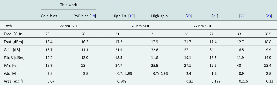
The key results obtained from single tone power sweep measurements are listed in Table 1. The PA has been reported in [Reference Rusanen, Hietanen, Sethi, Rahkonen, Pärssinen and Aikio18], but with bias setting that maximizes PAE and with pad losses removed from the results (see results “PAE bias” in Table 1). Here the main focus was to maximize gain and output power and thus completely different bias settings were used (See results “Gain bias” in Table 1).
Reference PA compared to state-of-the-art Ka-band PAs
Low noise amplifier
LNA design starts from topology choice, for mmWave frequencies, mainly two categories are used: common source and cascode topology. Common source topology has good noise and gain performance at a cost of lower isolation and stability. In turn, cascode topology has slightly worse gain and noise properties but it was chosen for its better stability. [Reference El-Aassar and Rebeiz24–Reference Li, El-Aassar, Kumar, Boenke and Rebeiz27].
LNA schematic diagram is shown in Fig. 6. To match LNA simultaneously to source impedance of 50 Ω and optimum noise impedance seen by LNA input, a source degeneration inductor (L1) is used together with input matching inductor (L2) and capacitor (C3). Cascode core composes of M1 which acts as a common source gain stage followed by a common gate stage M2, which gate is ac-grounded with C2. The output is loaded with a parallel LC-resonant tank (C1 and L3) for desired center frequency and output is matched to 50 Ω with L4 and C5. C4 is a DC-block capacitor allowing easy integration of possible future second stage. The DC-block capacitor is omitted from the input to minimize input losses that have a large impact on noise figure since mmWave antennas are typically patch antennas with no DC-path to ground.
Source degenerated cascode LNA schematic diagram.

The design of the LNA starts from choosing values for L1, L3, and transistor widths. 70 pH was chosen for degeneration inductor together with 120 pH for load inductor to have provided stable gain. A higher ratio of L3 to L1 results in higher gain at a cost of stability. Next, core is biased to conduct $150\, {\rm {{\rm \mu }}A}/\, {\rm {\mu }m}$ for optimum noise performance. Then load resonator is tuned to correct frequency with C1 after which noise and gain circles can be simulated to determine values for input matching network components. Lastly, the output matching network is dimensioned and LNA is characterized. This design procedure was repeated for multiple transistor widths to find an optimum width using a schematic model of the LNA using design kit capacitor models, pre-layout estimates of transistor parasitics and using a finite Q of 18 for all inductors. Table 2 shows a sweep of transistor size and simulated performance. As transistor width is increased, linearity improves and input matching inductor size reduces. $30\, {\rm {{\rm \mu }}m}$
 was chosen for optimal noise and gain performance. Simulations of designed LNA predict stable behavior from stability factors K, μ, and Δ which are all within stable values (K > 1, μ > 1, and Δ > 0).
LNA cascode core transistor sweep and simulated pre-layout performance

A micrograph of manufactured LNA is shown in Fig. 7. Matching inductor values were adjusted to compensate for added parasitic inductances from pads input feed, core input and ground return path. To support front-end integration, C3 (8fF) was replaced with a shunt switch (M3) of equal capacitance with negligible impact on performance. To check robustness for the front-end environment, a simulation was done feeding power to LNA input and a parallel 50 Ω load modeling an antenna. At 28 GHz the switch can withstand 18 dBm of PA power holding voltage swings below 0.8 V. Lastly, connections were routed out from LNA core from the back-gates of the transistors in order to study possible performance enhancements possibilities. In this process, transistors have the back-gate option, which allows threshold voltage tuning with roughly 80 mV/V sensitivity.
Reference LNA schematic diagram and micrograph.

On-wafer measurements for S-parameters and 1-tone compression were conducted using Keysight N5247A (PNA-X) with Cascade Microtech 40 GHz GSG probes. Noise figure was measured with noise source 346CK01, preamplifier U7228F and UXA signal analyzer N9040B with noise figure option (all Keysight equipment). Back-gate effects were studied by sweeping back-gates of amplifier transistors one by one while keeping bias current constant with the front gate of M1. Cascode transistor back-gate sweep is shown in Fig. 8(a). We observe improvement in gain (0.15 dB), linearity (1 dB) and noise figure (0.11 dB) when back-gate voltage is increased from 0 to 2 V. This is because the voltage drop is being equalized between the two transistors meaning there is more gain and more headroom in the output signal swing. Above 2 V, the voltage drops over M1 and M2 go off-balance resulting in a greatly degrading gain. Sweeping the input transistor (Fig. 8(b), back-gate does not show much changes, the optimum gain point is with negative back-gate voltage with a small cost of linearity. Gain-wise optimum bias setup was found to be of V bg1 = −0.4 V, V bg2 = 0.9 V, and V bias = 0.5 V which consumes 5.7 mA with 0.8 V supply or 190 μA/ μm of bias current. Gain optimum bias setup is compared to bias setup with no back-gates (backgates at 0V) in Fig. 8(c). At peak gain frequency, gain is improved by 0.2 dB, compression point by 0.36 dB and noise (from simulations) 0.07 dB. S-parameter results of this optimum gain bias setup is presented in Fig. 9 showing 8.7 dB of gain and 3 dB of noise figure. The circuit was modeled with parasitics extractor tool up to highest digital routing metal layer and thick metals were EM-modeled using Keysight Momentum. Measurements and simulations have good agreement with only a small discrepancy in output matching capacitor and load resonator capacitor capacitances. Lower gain and noise performance (3 dB) from initial simulations (Table 2) arise from parasitics of transistor core and lower Q-figures (about 15) for inductors.
Reference LNA back-gate experiments with constant bias current of 0.19 mA/ μm adjusted with front-gate bias. (a) Cascode back-gate sweep, (b) Input transistor back-gate sweep and c) Optimum back-gate bias setup of V bg1 = −0.4 V, ~ V bg2 = 0.9 V, V bias = 0.5 Vcompared to 0 V back-gates and V bias = 0.475 V. Solid plots are measurement results and dashed are acquired from simulations.

Reference LNA measured and simulated S-parameters and noise figure.

LNA is compared to other state-of-the-art Ka-band LNAs in Table 3. State-of-the-art LNAs have better gain and noise behavior but at cost of power dissipation. Reported references mostly utilize higher than nominal supply voltages to improve gain, noise and linearity, whereas we used nominal 0.8 V supply for easier integration for possible future systems (no need for an additional supply voltage for the chip).
Reference LNA compared to state-of-the-art Ka-band CMOS LNAs

Front-end
Combining LNA and FE into a front-end requires a few changes from reference amplifiers and results in the minimal additional area as we can see from Fig. 10 front-end micrograph. First, the output of PA and input of LNA have to be shifted by 90° to combine the nets into one. Second, LNA bias needs to be prevented from leaking to PA output matching ground by adding a DC-block, which in this case was put in PA output transformer (C6 in Fig. 10) as it did not take any additional area and its impact on TX and RX performance is insignificant as its value is high. Due to the changed impedance environment for both LNA and PA, their matching networks had to be slightly adjusted. LNA input inductor (L2) had to be increased from 660 to 710 pH to optimize noise match and in turn, PA output was compensated with C4 increase from 430 to 760 fF. Capacitance increase compensates the PA gain loss from LNA addition at a small cost of efficiency and saturated output power level. The robustness of the switch was again tested in the simulator by driving the PA at saturated power and checking voltage swings over the switch while sweeping antenna impedance in the Smith chart. Voltage swings stayed well within 0.8 V up to 1:8 of VSWR.
Front-end schematic diagram and micrograph.

To study how the impedance environment changes due to front-end integration, matches for both amplifiers were analyzed from S-parameter measurements and simulations. For minimum switch loss, both amplifiers would have to appear as 0 dB matches for each other in respective transmit and receive modes. Changes in impedance levels for reference amplifiers at antenna port are illustrated in Figs 11 and 12. For these figures, input feeds were de-embedded from measurement results using on-chip reflect impedance standards. In front-end simulations, the feeds were removed and the connection to the loading amplifier side was cut to model the front-end environment more accurately when looking directly at LNA input and PA output. For LNA, we get a quite good increase of impedance levels (−5.5 to −2 dB) due to large input inductor and grounding shunt switch. However, hand calculation with 25 Ω switch resistance and 710 pH L2 predict nearly 1 dB higher match:


Input matches of reference LNA (measured) and front-end LNA (simulated) with switch in receive mode (SW OFF), and in transmit mode (SW ON) in dB scale (a) and in Smith chart (b).

Output matches of reference PA (measured) and front-end PA (simulated) in on and off state in dB scale (a) and in Smith chart (b). Arrows illustrate the changes from PA to FE PA.

Difference in matching between theory and practice potentially comes from limited Q of the inductor and its parasitic capacitances. PA output match in front-end turned out to be worse upon integration. Switching PA off improves impedance levels in LNA point of view only by small amount, however, turning PA completely off eliminates any noise it generates since there is only little isolation from PA core to LNA input.
RX measurements
Measurement results for receive side are shown in Fig. 13. Due to leakage of signal to TX side, the LNA gain and noise figure have degraded about 2 dB below 26 GHz and due to resonance in TX side, gain and noise figure degrade rapidly above 28 GHz. Fig. 13(b) shows that back-gate study from LNA measurements apply also for front-end RX. Optimum back-gate settings improve gain and compression point. RX is providing peak gain of 7 dB with minimum NF of 5 dB with input compression point of −9.1 dBm.
RX S-parameter (a) and 1-tone measurement (b) results. S-parameter results are in optimum gain bias setup and zero back-gate bias compression point and gain are compared in right plot.

TX measurements
TX 1-tone measurements show degradation due to switch arrangement compared to reference PA. Measurement results at 28 GHz in Fig. 14(a) indicates that the switch lowers compression point by about 5 dB and saturated output power by only 2 dB. Non-linear load caused by the switch transistor M6 and LNA also results in an impact on AM/PM behavior with respect to the reference PA but only by a few degrees. Modification to matching capacitor C4 and parallel RX side has also changed the output center frequency from 28 to 26 GHz and bandwidth extension is observed due to de-Q of PA output matching environment in Fig. 14(b). Resulting gain, 1 dB compression point and saturated output power at 28 GHz are 15 dB, 7.4 dBm and 13.6 dBm, respectively.
Measured PA and TX 1-tone responses at 28 GHz (left) and saturated power comparison.

To study the linearity of the front-end in realistic 5G application, modulated signal measurements were carried out using 100 MHz wide cyclic prefix – orthogonal frequency division multiplexing (CP-OFDM) 64-QAM modulated signal following the 3GPP/NR standard for FR2 frequency band. 5G specifications for FR2 band limit adjacent channel power ratio (ACPR) to −28 dBc and error vector magnitude (EVM) to 8% [30]. To maximize channel power, digital predistortion (DPD) was used for the modulated signal. The signal was generated with Keysight M8190A Arbitrary waveform generator and then up-converted to 28 GHz by Keysight E8267E signal generator. The output of the front-end was then measured with Keysight N9040B UXA which analysed the ACPR and EVM. ACPR and EVM measurements are shown in Fig. 15. Resulting specification limited maximum channel power was measured to be 4.8 dBm which is close to 9 dB maximum practical back-off from saturated output power for the 64-QAM OFDM signal so all available output power is possible to utilize with the DPD. EVM of 7.6% leaves about 2.5% (−32 dBV) for rest of the transmitter chain, such as local oscillator phase noise, I/Q imbalance, thermal noise and data converter non-idealities, which is challenging but doable task to implement at mmWave frequencies.
ACPR and EVM of TX with swept input power with 100 MHz 64-QAM signal at 28 GHz. 5G specifications for ACPR and EVM are highlighted. Input and output powers are reported as channel average power.

Constellation diagrams and spectrums for maximum achievable channel power and 1 dB below maximum power are shown in Figs 16 and 17. Despite degraded linearity from front-end integration, the front-end meets the EVM specification without DPD with only 1 dB lower signal power (Fig. 16(a) however ACPR remains as a bottleneck.
Measured constellations of TX with maximum in-specification power (bottom) and with 1 dB lower input power. Left constellations are without DPD and right constellations are with DPD.

Output spectrum of TX with and without DPD. (a) is with input power 1 dB below maximum in-specification power and (b) is with maximum in-specification output power.

Comparison and discussion
The front-end key performance metrics are shown and compared to other Ka-band front-ends in Table 4. Simple switch technique results among the most compact front-end designs with comparable output power, efficiency and noise performance with exceptionally low RX power dissipation. Cascode is clearly the most popular LNA topology. Even though some front-ends have common source LNA, it is difficult to distinguish the topology from performance due to various switch techniques, number of stages and technology. That can not be said on PA topologies where the common trend is a couple dB power increase per increased stack number. Our design, unfortunately, suffers from lower output power due to switch non-linearity and gain preferred PA matching. Simulations show that reverting back to reference PA value for C4 and boosting PA VDD up to 3.5 V would regain reference PA compression point but with large power dissipation of 456 mW and reliability risks related to high VDD. Theoretical 3dB increase in signal power due to differential structures is evident from comparable output power of differential CS stages (1-stack) but at the cost of power and area.
Comparison of mmWave TDD front-ends. Reported frequency range is 3 dB bandwidth

$^{\rm {a}}$ complete TX/RX chain.
$^{\rm {b}}$ estimated from pPAE,P1 dB and gain.
$^{\rm {c}}$ at P1 dB.
$^{\rm {d}}$ estimated from micrograph.
On basis of measurement results, it is evident that performance is good below 26 GHz (see flat NF behavior in Fig. 13(a). So the designing of higher center frequencies of individual amplifiers might be beneficial so the lower frequency band can be utilized more readily. Additionally, instead of preferring gain, front-end PA matching should be done in more favor of power, and then compensating the lost gain with pre-driver PAs. In this way, the PA output impedance is potentially higher resulting in better isolation to the RX side. To combat the low TX compression point, M6 switch width could be increased but the increase of off-state capacitance would degrade LNA noise matching in RX-mode. Also reducing the widths of LNA transistors would result in a larger gate inductor (see Table 2) resulting in better isolation of RX side from TX, again with some noise penalty, while optimizing inductor Q.
Conclusion
We have presented a minimum area solution for a Ka-band TDD PA, LNA and switch front-end utilizing LNA matching network with shunt switch. Front-end switch performance was evaluated by comparing front-end performance to standalone reference amplifiers presented in this paper. TX provides 13.6 dBm of saturated output power at 28 GHz proving only 2 dB loss in output power and 4.8 dBm of channel power with 5G NR FR2 100 MHz wide OFDM signal with 9 dB backoff. At 24 GHz, the receive noise figure is 5 dB and gain 7 dB which are only 2 dB lower than of reference LNA relying on high impedance of an off-state PA. The paper also presents measurement and simulation results of back-gate option in used 22 nm FDSOI technology for LNA to improve gain and linearity. Possible improvements are discussed to decrease switch arrangement losses on overall performance. Active area (0.19 mm2) and first stage LNA power dissipation (4.6 mW) of the front-end is among the smallest reported to the author's best knowledge.
Acknowledgment
This research has been financially supported by the Academy of Finland 6Genesis Flagship (grant 318927) and Nokia Corporation Ltd. GLOBAL FOUNDRIES is acknowledged for silicon fabrication and technical support.
 Mikko Hietanen received his M.Sc. degree in 2018 and is currently pursuing his Ph.D. degree in Electrical eEngineering at the University of Oulu, Finland. He has worked on millimeter-wave frequency dividers and RF front-ends with 22 and 45 nm CMOS SOI processes. Before working on RFICs at the University of Oulu, he had an internship period in ESA specializing on on-wafer gallium-nitride device characterization.
 Jere Rusanen received his M.Sc. (Tech.) degree in Electrical Engineering in 2014 and is currently a doctoral student at the University of Oulu, Finland. During 2014–2019 he worked as an Antenna Engineer at Nokia, Oulu. His research interests include integrated millimeter wave power amplifiers.
 Janne P. Aikio was born in Haukipudas, Finland, in 1977. He received his M.Sc. and Ph.D. degrees in Electrical Engineering from the University of Oulu, Oulu, Finland, in 2002 and 2007, respectively. He is currently a Postdoctoral Researcher with the University of Oulu. His technical interests lie in the field of millimeter-wave integrated power amplifiers and modeling and analysis of distortion of RF power amplifiers.
 Nuutti Tervo (S’16) received his B.Sc. (Tech.) and M.Sc. (Tech.) degrees in Electrical Engineering from the University of Oulu in 2014, where he is currently pursuing the PhD degree with the Centre for Wireless Communications (CWC) research unit. He has a strong background in different fields of wireless communications including RF, radio channel modeling, signal processing, and system-level analysis. Around those topics, he has already authored or co-authored 35 international journal and conference papers. His PhD dissertation research focuses on nonlinearity and linearization of millimeter-wave beamforming transceivers.
 Timo Rahkonen was born in Jyvaskylä, Finland, 1962. He received his Diploma Engineer, Licentiate, and Doctor of Technology degrees in 1986, 1991 and 1994, respectively, at the University of Oulu, Finland. Currently, he is a professor in circuit theory and circuit design at the University of Oulu, Oulu, Finland, conducting research on linearization and error correction techniques for RF power amplifiers and A/D and D/A converters.
 Aarno Pärssinen received his D.Sc. degree from the Helsinki University of Technology in 2000. From 1994 to 2000 he was with Electronic Circuit Design Laboratory, Helsinki University of Technology, Finland, working on direct conversion receivers. In 1996, he was a Research Visitor at the University of California at Santa Barbara. From 2000 to 2011 he was with Nokia Research Center. During 2009–2011 he served as a member of Nokia CEO Technology Council. From 2011 to 2013, he was at Renesas Mobile Corporation working as a Distinguished Researcher and RF Research Manager. From October 2013 to September 2014 he was an Associate Technical Director at Broadcom. Since September 2014 he has been with the University of Oulu, Centre for Wireless Communications, Oulu, Finland where he is currently a Professor. His research interests include wireless systems and transceiver architectures for wireless communications with special emphasis on the RF and analog integrated circuit and system design.


 Open access