

1 Introduction
In the past decade, liquid crystal spatial light modulators (LCSLMs) have been widely used in panel display, beam control, adaptive optics, laser processing and other fields because it can precisely control the beam amplitude, wavefront, polarization and other parameters by changing the effective birefringence of liquid crystals[ Reference Wu and Yang 1 – Reference Hayasaki, Sugimoto, Takita and Nishida 5 ]. In addition, LCSLM is also widely used in the field of high-power lasers. Large aperture liquid crystal wave plates have been successfully applied in high-power laser systems[ Reference Jacobs, Cerqua, Marshall, Schmid, Guardalben and Skerrett 6 ]. It is reported that some liquid crystal devices have been used for more than 15 years, but the performance is still not significantly degraded. LCSLMs have been used in American NIF[ Reference Spaeth, Wegner, Suratwala, Nostrand, Bude, Conder, Folta, Heebner, Kegelmeyer, MacGowan, Mason, Matthews and Whitman 7 ] and China’s ‘Shenguang’[ Reference Huang, Fan, Li and Lin 8 – Reference Huang, Fan, Cheng, Xia, Pei, Li and Lin 10 ] for beam shaping and shielding damage points. However, when the laser power reaches a high intensity, the performance of the device will degrade. Because some materials in the structure of liquid crystal devices have a certain absorption of laser[ Reference Vladimirov, Pletneva, Soms and Pokrovskiy 11 ], this actually determines the damage threshold of LCSLMs.
The commonly used LCSLMs can be divided into many types. According to the function of the spatial light modulator (SLM), they can be divided into phase type and amplitude type[ Reference Weiner 12 ], and according to the addressing mode, they can be divided into electrically addressed spatial light modulators (EASLMs) and optically addressed spatial light modulators (OASLMs)[ Reference Shrestha, Chun and Chu 13 ]. However, no matter what type of LCSLM, indium tin oxide (ITO) and polyimide (PI) are essential in most cases. It is reported that the main heat source of LCSLMs under laser irradiation is the ITO layer, followed by the PI layer[ Reference Tuna, Selamet, Aygun and Ozyuzer 14 , Reference Wang, Huang, Zhang, Luo, Huang, Li, Luo, Wang and Zhao 15 ]. Moreover, the twisted nematic (TN) liquid crystal commonly used in LCSLM is very sensitive to the operating temperature[ Reference Garcia-Marquez, Lopez, Gonzalez-Vega and Noe 16 ], which leads to the degradation of the performance of LCSLMs after temperature rise. In order to solve this problem, there are many studies on phase-type EASLM. Watson et al. pointed out that this is caused by the thermal expansion and cold contraction of sealant under the action of temperature, resulting in the inability of liquid crystals to completely fill the volume between glass substrates[ Reference Watson, Whitaker and Harris 17 ]. Cao et al. reported that the increase of temperature led to the phase transition of liquid crystals and changed the light intensity in the laser irradiation area[ Reference Cao, Mu, Hu, Liu and Xuan 18 ]. He et al. established the SLM model and believed that the temperature affects the refractive index and rotation angle of liquid crystal molecules[ Reference He, Wang, Wu, Tan, Li, Shang, Wu and Huang 19 , Reference Zhou, Wang, Zhuo, He, Wu, Wang, Tan and Qiu 20 ]. Zhu et al. believed that the performance degradation is caused by the change of liquid crystal cell thickness due to temperature rise[ Reference Zhu, Whitehead, Perrie, Allegre, Olle, Li, Tang, Dawson, Jin, Edwardson, Li and Dearden 21 ].
In addition to the research on phase-type EASLMs, the demand for high-power laser for amplitude-type OASLMs is also increasing. LLNL reports that the printing speed can be greatly improved by using OASLM for surface scanning printing[ Reference Matthews, Guss, Drachenberg, Demuth, Heebner, Duoss, Kuntz and Spadaccini 22 ]. The developed OASLM has been used for beam shaping of fusion-level laser systems[ Reference Heebner, Borden, Miller, Hunter, Christensen, Scanlan, Haynam, Wegner, Hermann, Brunton, Tse, Awwal, Wong, Seppala, Franks, Marley, Williams, Budge, Henesian, Stolz, Suratwala, Monticelli, Walmer, Dixit, Widmayer, Wolfe, Bude, McCarty and DiNicola 23 , Reference Heebner, Borden, Miller, Stolz, Suratwala, Wegner, Hermann, Henesian, Haynam, Hunter, Christensen, Wong, Seppala, Brunton, Tse, Awwal, Franks, Marley, Williams, Scanlan, Budge, Monticelli, Walmer, Dixit, Widmayer, Wolfe, Bude, McCarty and DiNicola 24 ]. The system can improve the service life of optical elements by shielding damage points. The LMJ in France adopts a design similar to NIF to form a laser in the injection laser system to compensate for the gain distribution of the main amplifier[ Reference Luce 25 ]. Cai et al.3 reported that surface scanning additive manufacturing can be carried out by using an OASLM[ Reference Cai, Huang, Cheng, Xia and Fan 26 ], which has good development potential for metal printing. With the development of high-repetition-rate laser, it is obvious that amplitude-type OASLMs also face the problem of thermal degradation, which will limit their wide application. However, there are a few reports on the damage mechanism and optical properties of amplitude-type OASLMs irradiated by high-repetition-frequency or continuous laser. Therefore, it is of great significance to study the performance of amplitude-type OASLMs under continuous irradiation of high-power laser.
In this paper, we build a laser-induced model based on the OASLM of a Bi12SiO20 (BSO) crystal to evaluate the thermal effect of the OASLM under high-power continuous wave (CW) laser. On this basis, the effect of temperature on the transmittance of OASLMs is studied. The results show that the transmittance of an OASLM increases with the increase of temperature. The threshold voltage and saturation voltage of the liquid crystal layer decrease with the increase of temperature, and the degree to which they decrease is different. In order to meet the threshold voltage and saturation voltage of the liquid crystal layer at the same time, we propose to use the photoelectric characteristics of BSO, where the partial voltage of the liquid crystal layer is lower in low gray coding mode and higher in high gray coding mode, so as to meet two conditions at the same time to compensate for the on–off ratio degradation of the OASLM. Finally, by adjusting the driving voltage of the liquid crystal light valve and output intensity of the optical writing module, the OASLM can operate normally for a long time under high-power CW laser irradiation without any external heat dissipation measures.
2 Theory
2.1 Laser-induced heat transfer model
As a kind of transmission device[ Reference Huang, Fan, Li and Lin 8 ], a schematic diagram of laser irradiation in practical use of an OASLM is shown in Figure 1. Different from the EASLM, it can control the intensity distribution by controlling the spatial intensity of the 470-nm addressed beam, which will alter the resistance of the BSO crystal and realize the voltage division in different regions. There is only one layer of ITO adjacent to the liquid crystal, and another layer of ITO is moved to the outside of the BSO, which will be different from the temperature distribution of an EASLM. Under the irradiation of CW laser, the whole device is a steady-state model, which needs to consider the internal thermal diffusion of the device.
(a) Heat transfer equation model. (b) Structure diagram of a laser-irradiated OASLM.

Therefore, in order to analyze the thermal effect of an OASLM under a CW laser, the heat transfer model of this structure should be discussed first. It can be considered that each layer of an OASLM is a heat source for absorbing laser energy. For a single-wavelength, parallel incident laser, which experiences little refraction, reflection and scattering in the material, the absorption of laser energy can be analyzed by the Beer–Lambert law. The thermal distribution model of an OASLM irradiated by high-power CW laser at 1064 nm can be written as the following differential form:
 $$\begin{align}\frac{\partial I}{\partial Z}=\alpha I\left(1-R\right),\end{align}$$
where $I$
is the intensity of the incident laser,
$I$
is the intensity of the incident laser, $Z$
is the depth of the material,
$Z$
is the depth of the material, $\alpha$
represents the absorption coefficient of the 1064 nm laser, and
$\alpha$
represents the absorption coefficient of the 1064 nm laser, and $R$
is the surface reflectivity of the OASLM to laser. After thermal deposition, the heat will change in space and time scales. It is necessary to solve the temperature distribution inside the material. As shown in Figure 1(a), the partial differential equation of temperature distribution in the material is as follows:
$R$
is the surface reflectivity of the OASLM to laser. After thermal deposition, the heat will change in space and time scales. It is necessary to solve the temperature distribution inside the material. As shown in Figure 1(a), the partial differential equation of temperature distribution in the material is as follows:
 $$\begin{align}\rho C\frac{\partial T}{\partial t}-\frac{k}{r}\frac{\partial }{\partial r}\left(\frac{\partial T}{\partial r}\right)-k\frac{\partial^2T}{\partial {z}^2}=Q=\alpha I\left(1-R\right),\end{align}$$
where $\rho$
,
$\rho$
, $C$
and
$C$
and $k$
are the density, specific heat capacity and thermal conductivity of the material, and
$k$
are the density, specific heat capacity and thermal conductivity of the material, and $Q$
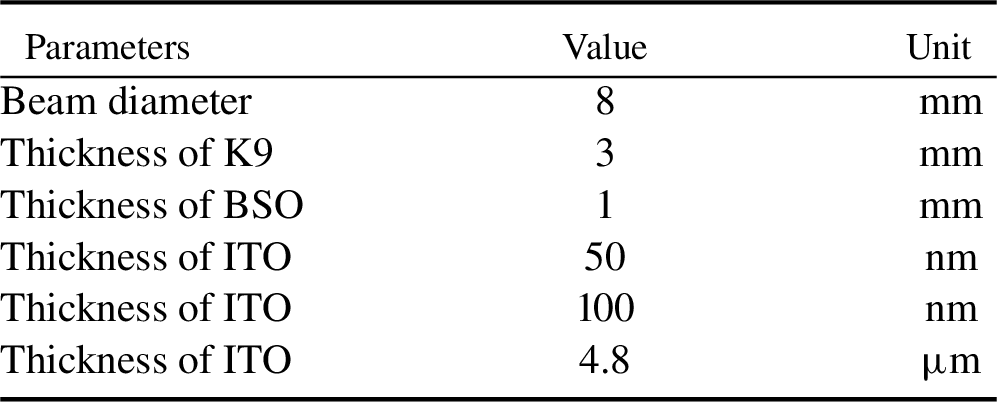
is the bulk heat source generated by the material absorbing laser energy. According to the geometric properties of the OASLM structure layer, as shown in Figure 1(b), there are several antireflective films in the actual structure. Because these films have little absorption of laser and are very thin, their heat transfer can be ignored. The marked parts are all key structures and are essential. A laser-induced heat transfer model is established by finite-element analysis. Because the laser is incident from the front of the OASLM, in order to simplify the model, the symmetry of the structure is used to reduce the size of the model, which only investigates 1/4 of the OASLM, as shown in Figure 2. The heat source region represents the part where the laser interacts with the material. The investigation part is the actual heat transfer model. The heat distribution model can be successfully established by setting the boundary conditions and the physical parameters of the material. The physical parameters of each material are listed in Table 1.
$Q$
is the bulk heat source generated by the material absorbing laser energy. According to the geometric properties of the OASLM structure layer, as shown in Figure 1(b), there are several antireflective films in the actual structure. Because these films have little absorption of laser and are very thin, their heat transfer can be ignored. The marked parts are all key structures and are essential. A laser-induced heat transfer model is established by finite-element analysis. Because the laser is incident from the front of the OASLM, in order to simplify the model, the symmetry of the structure is used to reduce the size of the model, which only investigates 1/4 of the OASLM, as shown in Figure 2. The heat source region represents the part where the laser interacts with the material. The investigation part is the actual heat transfer model. The heat distribution model can be successfully established by setting the boundary conditions and the physical parameters of the material. The physical parameters of each material are listed in Table 1.
Physical parameters of structural materials.

Simplified heat transfer model.

2.2 Effect of temperature on optical properties
The effective birefringence of liquid crystal changes with the increase of temperature. The temperature-dependent birefringence can be expressed as[ Reference Li, Gauza and Wu 27 ]
 $$\begin{align}{n}_{\mathrm{e}}(T)=A- BT+\frac{2}{3}{\left(\Delta n\right)}_0{\left(1-\frac{T}{T_{\mathrm{C}}}\right)}^{\beta },\end{align}$$
 $$\begin{align}{n}_{\mathrm{o}}(T)=A- BT-\frac{1}{3}{\left(\Delta n\right)}_0{\left(1-\frac{T}{T_{\mathrm{C}}}\right)}^{\beta },\end{align}$$
where ${n}_{\mathrm{e}}$
and
${n}_{\mathrm{e}}$
and ${n}_{\mathrm{o}}$
are the extraordinary index and the ordinary index,
${n}_{\mathrm{o}}$
are the extraordinary index and the ordinary index, $A$
and
$A$
and $B$
are the temperature-related parameters at a given wavelength, and the specific values can be solved through multiple sets of data measurement,
$B$
are the temperature-related parameters at a given wavelength, and the specific values can be solved through multiple sets of data measurement, ${\left(\Delta n\right)}_0$
is the effective birefringence of the liquid crystal in the crystal state (or T = 0 K),
${\left(\Delta n\right)}_0$
is the effective birefringence of the liquid crystal in the crystal state (or T = 0 K), $T$
is the actual temperature of the liquid crystal,
$T$
is the actual temperature of the liquid crystal, ${T}_{\mathrm{C}}$
is the clear point temperature of the liquid crystal, and
${T}_{\mathrm{C}}$
is the clear point temperature of the liquid crystal, and $\beta$
represents the material constant of the liquid crystal. The liquid crystal studied in this paper is E7 type of which
$\beta$
represents the material constant of the liquid crystal. The liquid crystal studied in this paper is E7 type of which $\beta$
is about 0.14–0.2.
$\beta$
is about 0.14–0.2.
By subtracting Equation (4) from Equation (3), the following relation between the birefringence index and temperature of the liquid crystal can be obtained:
 $$\begin{align}\Delta n(T)={\left(\Delta n\right)}_0{\left(1-\frac{T}{T_{\mathrm{C}}}\right)}^{\beta }.\end{align}$$
The structure of amplitude-type OASLM is that the alignment of liquid crystal is twisted by 90° through the PI orientation layer. When a linearly polarized laser beam is incident vertically, the polarization of the output light passing through the liquid crystal cell will rotate by 90°. The angle of polarization rotation can be adjusted by adjusting the electric field intensity of liquid crystal, and combining with the polarizer behind the liquid crystal valve, the laser intensity modulation can be realized. In this case, the laser intensity through OASLM can be expressed as follows[ Reference Gooch and Tarry 28 ]:
 $$\begin{align}I={I}_0\left(1-R\right){\sin}^2\kern-2pt\left(\kern-2pt\frac{\pi }{2}\sqrt{1\kern-1pt +\kern-1pt{\left(\kern-1pt\frac{2\Delta nd}{\lambda}\right)\kern-2pt}^2}\right)\kern-2pt\bigg/\kern-2pt\left(\kern-2pt1+{\left(\frac{2\Delta nd}{\lambda}\right)}^2\right),\end{align}$$
where ${I}_0$
is the incident laser intensity and
${I}_0$
is the incident laser intensity and $d$
is the thickness of the liquid crystal layer. Substituting Equation (5) into Equation (6), the relationship between intensity and temperature can be further obtained as follows:
$d$
is the thickness of the liquid crystal layer. Substituting Equation (5) into Equation (6), the relationship between intensity and temperature can be further obtained as follows:
 $$\begin{align}I={I}_0\left(1-R\right){\sin}^2\left(\frac{\pi }{2}\sqrt{N}\right)/N,\end{align}$$
 $$\begin{align}N=1+{\left(\frac{2{\left(\Delta n\right)}_0{\left(1-T/{T}_{\mathrm{C}}\right)}^{\beta }d}{\lambda}\right)}^2.\end{align}$$
The above equation only analyzes the effect of temperature on the transmitted laser intensity, without considering the effect of electric field. When an OASLM works, an electric field will be applied to the liquid crystal layer, and the birefringence of the liquid crystal can be expressed as follows[ Reference Lin, Feng and Chen 29 ]:
 $$\begin{align}\Delta n&\approx {\Delta n}_0-\left(\frac{U_{\mathrm{LC}}-{U}_{\mathrm{th}}}{U_{\mathrm{th}}}\right), \nonumber\\ {\Delta n}_0&=\left(\frac{2\pi m{\left(1-T/{T}_{\mathrm{C}}\right)}^{\frac{\beta }{2}}-{U}_{\mathrm{LC}}}{\pi m{\left(1-T/{T}_{\mathrm{C}}\right)}^{\frac{\beta }{2}}}\right){\Delta n}_0,\end{align}$$
where ${U}_{\mathrm{LC}}$
is the voltage applied to the liquid crystal layer,
${U}_{\mathrm{LC}}$
is the voltage applied to the liquid crystal layer, ${U}_{\mathrm{th}}$
is the threshold voltage of the liquid crystal,
${U}_{\mathrm{th}}$
is the threshold voltage of the liquid crystal, $m$
is a parameter related to the elastic coefficient, and
$m$
is a parameter related to the elastic coefficient, and ${\Delta n}_0$
is the birefringence without an applied electric field (or
${\Delta n}_0$
is the birefringence without an applied electric field (or ${U}_{\mathrm{LC}}<{U}_{\mathrm{th}}$
). Here
${U}_{\mathrm{LC}}<{U}_{\mathrm{th}}$
). Here ${U}_{\mathrm{th}}$
represents the critical voltage for the deflection jump of liquid crystal molecules, and the applied electric field does not work until it is higher than it. It is worth mentioning that only when
${U}_{\mathrm{th}}$
represents the critical voltage for the deflection jump of liquid crystal molecules, and the applied electric field does not work until it is higher than it. It is worth mentioning that only when ${U}_{\mathrm{th}}$
is slightly higher than
${U}_{\mathrm{th}}$
is slightly higher than ${U}_{\mathrm{LC}}$
can Equation (9) be established. As the difference between
${U}_{\mathrm{LC}}$
can Equation (9) be established. As the difference between ${U}_{\mathrm{LC}}$
and
${U}_{\mathrm{LC}}$
and ${U}_{\mathrm{th}}$
becomes too large, the small angle approximation will no longer be satisfied. The
${U}_{\mathrm{th}}$
becomes too large, the small angle approximation will no longer be satisfied. The ${U}_{\mathrm{th}}$
of the liquid crystal also changes with the temperature, which can be expressed as follows[
Reference Lin, Feng and Chen
29
]:
${U}_{\mathrm{th}}$
of the liquid crystal also changes with the temperature, which can be expressed as follows[
Reference Lin, Feng and Chen
29
]:
 $$\begin{align}{U}_{\mathrm{th}}=\pi m{\left(1-\frac{T}{T_{\mathrm{C}}}\right)}^{\beta /2}.\end{align}$$
The liquid crystal light valve in an OASLM is a series structure composed of ITO, BSO crystal and liquid crystal layer. The voltage of the liquid crystal layer is not directly loaded, but determined by the external driving voltage of the liquid crystal light valve and the partial voltage of the BSO crystal[ Reference Huang, Fan, Li and Lin 9 ]. The actual voltage of the liquid crystal layer can be expressed as
 $$\begin{align}{U}_{\mathrm{LC}}={U}_{\mathrm{AC}}\frac{\frac{1}{R_0}+\frac{1}{R_{\phi }}+ j\omega {C}_{\mathrm{BSO}}+\frac{j\omega {C}_1}{1+ j\omega {R}_1{C}_1}}{\frac{1}{R_0}+\frac{1}{R_{\phi }}+ j\omega {C}_{\mathrm{BSO}}+\frac{j\omega {C}_1}{1+ j\omega {R}_1{C}_1}+\frac{1}{R_{\mathrm{LC}}}+ j\omega {C}_{\mathrm{LC}}},\end{align}$$
where ${U}_{\mathrm{LC}}$
is the liquid crystal layer voltage,
${U}_{\mathrm{LC}}$
is the liquid crystal layer voltage, ${U}_{\mathrm{AC}}$
is the external driving voltage,
${U}_{\mathrm{AC}}$
is the external driving voltage, ${R}_0$
is the dark resistance of BSO,
${R}_0$
is the dark resistance of BSO, ${R}_{\phi }$
is the resistance of BSO exposed to the writing light, which changes with the intensity of the writing light, and
${R}_{\phi }$
is the resistance of BSO exposed to the writing light, which changes with the intensity of the writing light, and ${R}_1$
and
${R}_1$
and ${C}_1$
are the trapping effect resistance and capacitance of BSO crystal, respectively. The parameters can be calculated from the electrical properties of liquid crystal and the electrical impulse response of BSO.
${C}_1$
are the trapping effect resistance and capacitance of BSO crystal, respectively. The parameters can be calculated from the electrical properties of liquid crystal and the electrical impulse response of BSO.
By further processing the relationship between voltage and birefringence and the relationship between transmittance and refractive index, the relationship between transmittance and temperature under an applied voltage can be obtained, by substituting Equation (9) into Equation (8), as follows:
 $$\begin{align}& {N}_{U_{\mathrm{LC}}}=1 \nonumber \\ &\quad +{\left(\frac{2d{\Delta n}_0}{\pi m\lambda}\left(2\pi m{\left(1-\frac{T}{T_{\mathrm{C}}}\right)}^{\beta } -{U}_{\mathrm{LC}}{\left(1-\frac{T}{T_{\mathrm{C}}}\right)}^{\beta /2}\right)\right)}^2.\end{align}$$
The transmittance of OASLM under temperature and voltage can be obtained by solving Equation (12) as follows:
 $$\begin{align}{T}_{\mathrm{SLM}}=\frac{I}{I_0}=\left(1-R\right){\sin}^2\left(\frac{\pi }{2}\sqrt{N_{U_{\mathrm{LC}}}}\right)/{N}_{U_{\mathrm{LC}}},\end{align}$$
where ${T}_{\mathrm{SLM}}$
is the transmittance of the OASLM. When calculating the effect of temperature on transmittance,
${T}_{\mathrm{SLM}}$
is the transmittance of the OASLM. When calculating the effect of temperature on transmittance, ${U}_{\mathrm{LC}}$
is a given fixed value and
${U}_{\mathrm{LC}}$
is a given fixed value and ${\Delta n}_0$
is the birefringence at room temperature without an external electric field. According to Equations (12) and (13), when the voltage of the liquid crystal layer is constant, the transmittance of the OASLM increases with the increase of temperature.
${\Delta n}_0$
is the birefringence at room temperature without an external electric field. According to Equations (12) and (13), when the voltage of the liquid crystal layer is constant, the transmittance of the OASLM increases with the increase of temperature.
3 Numerical simulation and theoretical analysis
The external boundary of an OASLM in the laser-induced model is affected by air convection. For the surface exposed to air, the heat transfer coefficient is set as h = 5 W/(m2·K), the profile generated by the simplified model is set as a symmetrical boundary, and the ambient temperature is set as 298.15 K. According to the model parameters in Table 2, the laser beam has a Gaussian distribution, and the laser power density is set to 16 W/cm2. The steady-state temperature distribution on the y = 0 plane of the liquid crystal light valve is shown in Figure 3(a), where L represents the distance from the laser irradiation center (or L = x). The high-temperature
Physical parameters of structural materials.
(a) Temperature distribution on the y = 0 plane of a laser-induced liquid crystal light valve. (b) Temperature distribution along the transverse direction of an ITO layer, K9 layer and liquid crystal layer. (c) Temperature distribution along the depth direction at the center of a liquid crystal light valve, the small icon shows the material structure distribution along the Z direction.

region of the OASLM is concentrated in the BSO crystal region. This is because the BSO crystal has a certain absorption to the laser, and the ITO is in direct contact with air, so the thermal conductivity is low, and the heat cannot be dissipated in time. The temperature distributions of the ITO layer, liquid crystal layer and K9 substrate are shown in Figure 3(b), where ITO1 is the conductive film layer on the BSO crystal side, and the temperature of the liquid crystal layer is close to that of ITO in the liquid crystal light valve. The temperature in this region has a direct effect on the performance of the OASLM, and the maximum temperature difference between the K9 substrate and liquid crystal layer is about 4 K. Because of the Gaussian distribution of the beam, the temperature gradient is most obvious in the central region of laser irradiation, and gradually decreases along the horizontal direction. Figure 3(c) shows the temperature distribution in the depth direction of OASLM at the laser irradiation center, and the temperature increases uniformly from K9 side along BSO side. It can be seen that under irradiation by a high-power CW laser, the temperature of the liquid crystal light valve will far exceed the normal working temperature, which will affect the performance of the OASLM.
The temperature-induced degradation is mainly due to the change of birefringence which affects the transmittance of an OASLM. When the liquid crystal light valve is in the ‘OFF’ mode, this means the linearly polarized light passes through the TN liquid crystal cell and rotates 90°, and there is no light output after passing through the polarizer. The initial transmittance ${T}_{\mathrm{SLM}}$
= 0. As the temperature changes, the transmittance is affected by temperature by calculating Equations (12) and (13), as shown in Figure 4(a). In the analysis and calculation, the reflectivity R is not affected by the temperature and voltage and is a constant. For the convenience of calculation, we make R = 0. With the increase of temperature, the transmission rate of an OASLM increases gradually, and the transmittance increases sharply when it approaches the clear point (332 K), which makes the OASLM unable to modulate amplitude. In the process of temperature increase, the liquid crystal is mainly affected by the electric field and temperature, and the temperature affects the threshold voltage of the liquid crystal light valve. In order to ensure the normal voltage response of an OASLM, the
${T}_{\mathrm{SLM}}$
= 0. As the temperature changes, the transmittance is affected by temperature by calculating Equations (12) and (13), as shown in Figure 4(a). In the analysis and calculation, the reflectivity R is not affected by the temperature and voltage and is a constant. For the convenience of calculation, we make R = 0. With the increase of temperature, the transmission rate of an OASLM increases gradually, and the transmittance increases sharply when it approaches the clear point (332 K), which makes the OASLM unable to modulate amplitude. In the process of temperature increase, the liquid crystal is mainly affected by the electric field and temperature, and the temperature affects the threshold voltage of the liquid crystal light valve. In order to ensure the normal voltage response of an OASLM, the ${U}_{\mathrm{LC}}$
of the liquid crystal layer is usually required to be slightly higher than the threshold voltage
${U}_{\mathrm{LC}}$
of the liquid crystal layer is usually required to be slightly higher than the threshold voltage ${U}_{\mathrm{th}}$
. With the increase of temperature, the
${U}_{\mathrm{th}}$
. With the increase of temperature, the ${U}_{\mathrm{th}}$
of liquid crystal changes. Obviously, the voltage
${U}_{\mathrm{th}}$
of liquid crystal changes. Obviously, the voltage ${U}_{\mathrm{LC}}$
of the liquid crystal layer also needs to be adjusted, which needs to be realized by adjusting the external driving voltage
${U}_{\mathrm{LC}}$
of the liquid crystal layer also needs to be adjusted, which needs to be realized by adjusting the external driving voltage ${U}_{\mathrm{AC}}$
. According to Equations (10) and (11), the relationship between the driving voltage of an OASLM and the temperature is obtained, as shown in Figure 4(b). With the increase of temperature, the driving voltage begins to decrease until the liquid crystal reaches the clear point, and the effect of the electric field is no longer considered. It is worth mentioning that the damage performance of OASLM irradiated by a CW laser is different from that irradiated by a pulsed laser. Under high-power pulsed laser irradiation, an OASLM will produce unrecoverable physical damage points, which is limited by the damage threshold of ITO. Under high-power CW laser or quasi-CW laser, the thermal deposition of an OASLM leads to the degradation of equipment performance, which is recoverable damage and is limited to the clear point of the liquid crystal. Before that, the performance degradation caused by temperature can be compensated for by an electric field, which can allow the OASLM to be used more effectively.
${U}_{\mathrm{AC}}$
. According to Equations (10) and (11), the relationship between the driving voltage of an OASLM and the temperature is obtained, as shown in Figure 4(b). With the increase of temperature, the driving voltage begins to decrease until the liquid crystal reaches the clear point, and the effect of the electric field is no longer considered. It is worth mentioning that the damage performance of OASLM irradiated by a CW laser is different from that irradiated by a pulsed laser. Under high-power pulsed laser irradiation, an OASLM will produce unrecoverable physical damage points, which is limited by the damage threshold of ITO. Under high-power CW laser or quasi-CW laser, the thermal deposition of an OASLM leads to the degradation of equipment performance, which is recoverable damage and is limited to the clear point of the liquid crystal. Before that, the performance degradation caused by temperature can be compensated for by an electric field, which can allow the OASLM to be used more effectively.
(a) Relationship between transmittance and temperature of an OASLM. (b) The required adjustment of driving voltage with temperature.

In order to reduce the effect of temperature, the transmission change can be compensated for by adjusting the electric field of the liquid crystal layer. When the liquid crystal light valve is in the ‘OFF’ mode, and can respond to voltage, the voltage ${U}_{\mathrm{LC}}$
of the liquid crystal layer needs to be slightly higher than the threshold voltage
${U}_{\mathrm{LC}}$
of the liquid crystal layer needs to be slightly higher than the threshold voltage ${U}_{\mathrm{th}}$
. When the liquid crystal light valve is in the ‘ON’ mode, the voltage of the liquid crystal layer also needs to meet the saturation voltage, which is the voltage value that enables the liquid crystal molecules to deflect completely. It is necessary to reduce the voltage
${U}_{\mathrm{th}}$
. When the liquid crystal light valve is in the ‘ON’ mode, the voltage of the liquid crystal layer also needs to meet the saturation voltage, which is the voltage value that enables the liquid crystal molecules to deflect completely. It is necessary to reduce the voltage ${U}_{\mathrm{LC}}$
of the liquid crystal layer and meet the requirement of saturation voltage at the same time. In Equation (11), the factors that affect the liquid crystal layer voltage include the resistance
${U}_{\mathrm{LC}}$
of the liquid crystal layer and meet the requirement of saturation voltage at the same time. In Equation (11), the factors that affect the liquid crystal layer voltage include the resistance ${R}_{\phi }$
and driving voltage of the BSO crystal. The resistance
${R}_{\phi }$
and driving voltage of the BSO crystal. The resistance ${R}_{\phi }$
can be realized by adjusting the signal intensity of the writing beam, which is controlled by the driving current. The driving voltage and current of the OASLM in normal working state are 24 V and 600 mA, respectively. The voltage distribution of the liquid crystal layer under different driving voltage and driving current in each gray mode is calculated by Equation (11), as shown in Figure 5. Only reducing the driving voltage can obviously reduce the
${R}_{\phi }$
can be realized by adjusting the signal intensity of the writing beam, which is controlled by the driving current. The driving voltage and current of the OASLM in normal working state are 24 V and 600 mA, respectively. The voltage distribution of the liquid crystal layer under different driving voltage and driving current in each gray mode is calculated by Equation (11), as shown in Figure 5. Only reducing the driving voltage can obviously reduce the ${U}_{\mathrm{LC}}$
of the liquid crystal layer, but at the same time, the
${U}_{\mathrm{LC}}$
of the liquid crystal layer, but at the same time, the ${U}_{\mathrm{LC}}$
of the liquid crystal layer at each gray level is reduced. In particular, the saturation voltage decreases significantly, which makes the electric field of the liquid crystal light valve insufficient, resulting in a decrease of the transmittance of the OASLM. With the decrease of driving voltage and the increase of driving current of the writing light, the BSO crystal has higher resistance in low gray mode, and the
${U}_{\mathrm{LC}}$
of the liquid crystal layer at each gray level is reduced. In particular, the saturation voltage decreases significantly, which makes the electric field of the liquid crystal light valve insufficient, resulting in a decrease of the transmittance of the OASLM. With the decrease of driving voltage and the increase of driving current of the writing light, the BSO crystal has higher resistance in low gray mode, and the ${U}_{\mathrm{LC}}$
of liquid crystal layer is reduced as scheduled. The resistance
${U}_{\mathrm{LC}}$
of liquid crystal layer is reduced as scheduled. The resistance ${R}_{\phi }$
of the BSO crystal in high gray mode is smaller, so the liquid crystal layer can receive a higher voltage, the liquid crystal light valve can meet the saturation voltage, and the transmittance of the OASLM is guaranteed. The compensation process is shown in Figure 6. In addition, increasing the driving current of writing light only adjusts the intensity of the addressed blue LED and will not be directly loaded on the liquid crystal cell. The increased blue light intensity is not enough to damage the liquid crystal. However, increasing the driving current may reduce the service life of the blue LED.
${R}_{\phi }$
of the BSO crystal in high gray mode is smaller, so the liquid crystal layer can receive a higher voltage, the liquid crystal light valve can meet the saturation voltage, and the transmittance of the OASLM is guaranteed. The compensation process is shown in Figure 6. In addition, increasing the driving current of writing light only adjusts the intensity of the addressed blue LED and will not be directly loaded on the liquid crystal cell. The increased blue light intensity is not enough to damage the liquid crystal. However, increasing the driving current may reduce the service life of the blue LED.
Voltage of liquid crystal layer changes with the loaded gray level under different driving conditions.

Flow chart of the proposed compensation method.

4 Experimental system and results
Figure 7 shows the experimental measurement device. A CW fiber laser is used to irradiate the OASLM to study the variation of optical properties of the OASLM with increasing temperature. The amplitude-type OASLM (720 × 720) device used in the experiment is home-made[ Reference Huang, Fan, Li and Lin 8 – Reference Huang, Fan, Cheng, Xia, Pei, Li and Lin 10 ], the optical aperture is 22 mm × 22 mm, the transmittance is greater than 85% at 1064 nm, the switch ratio is greater than 100:1, the default driving voltage is 24 V, and the driving current is 600 mA. The central wavelength of the laser is 1064 nm, and the diameter of the spot irradiated on the OASLM is 8 mm. The driver is used to adjust the driving voltage and current of addressed beam. Polarizer 1 (POL1), polarizer 2 (POL2) and the half wave plate (HWP) are used to fine-tune the power of the read-out laser beam. The laser power density irradiated on the OASLM can be calculated by using a power meter. The thermal imager is used to detect the surface temperature liquid crystal light valve. The neutral density filter (NDF) is used to protect the CCD from damage. Polarizer 3 (POL3) and the analyzer (ANA) are aligned in parallel to make the OASLM output initially in the ‘OFF’ mode, and the CCD is used to detect the light field intensity distribution of the system.
Schematic diagram of the OASLM temperature rise performance test experimental system. POL: polarizer, HWP: half wave plate, BS: beam splitter, NDF: neutral density filter, L: lens, and ANA: analyzer.

When OASLM is in the ‘OFF’ mode, the CCD cannot detect the light intensity at normal operating temperature (298 K), and the transmittance of the device is zero. Detecting the temperature change of liquid crystal light valve under different laser power density, as shown in Figure 8(a), each result is obtained under long-term irradiation. The results show that the temperature increases with the increase of laser power density. Because there are no thermal management measures, when the power density reaches 23 W/cm2, the liquid crystal temperature reaches the clear point (332 K). In order to prevent the OASLM from not working so that it can be compensated for, it is more appropriate to set the laser power of subsequent experiments to 21 W/cm2. In the process of reaching the clear point from the ambient temperature, the light field intensity detected by CCD changes with the increase of the temperature of the liquid crystal light valve, which converts the light field intensity change into the transmittance change of the OASLM, as shown in Figure 8(b). The results show that the transmittance of OASLM increases continuously with the increase of temperature until the liquid crystal light valve loses its effect.
(a) Temperature of the OASLM as a function of laser power density. (b) Transmittance of the OASLM as a function of temperature, where the red data points are the experimental data and the blue curve is the fitting curve.

Through the previous theoretical calculation, the influence of temperature on the transmission of the OASLM can be compensated for by reducing the driving voltage. When the laser intensity is set to 21 W/cm2, the transmittance increases due to the temperature rise (326 K) of the OASLM. At this time, the OASLM cannot reach the ‘OFF’ mode, and the light field intensity distribution is shown in Figure 9(a). Then, by reducing the driving voltage for compensation, the change of the light field is shown in Figures 9(b) to 9(d), and the corresponding voltages are 22 V, 20 V and 19 V, respectively. The results show that the increase of transmittance caused by temperature is compensated for. The compensation voltage at different temperatures is recorded, and the relationship diagram shown in Figure 9(e) is obtained, which is basically consistent with the theoretical calculation results. In addition, in order to verify the influence of driving voltage and driving current on the transmittance of the OASLM under different operating temperatures, the relationship curve (gamma curve) between the transmittance and gray level of the OASLM under different gray levels is detected by CCD, as shown in Figure 9(f). Curve 1 is the gamma curve of the OASLM in normal operation (at 298–310 K). At this time, the power density of the laser is below 7.5 W/cm2, the driving voltage is 24 V and the driving current is 600 mA. Curve 2 shows the gamma curve when the temperature is increased to 326 K by laser irradiation and the power density of the laser reaches 21 W/cm2. In this case, the OASLM cannot work in black mode. By adjusting the driving voltage to 19 V, the gamma curve is shown in curve 3, which essentially reduces the threshold voltage of the liquid crystal light valve and enables the OASLM to be in the ‘OFF’ mode. However, the voltage of each gray level is reduced, resulting in a significant reduction in the overall transmittance of OASLM, which seriously affects the utilization of the laser. Through the analysis of the results in Figure 5, when the driving current is increased to 1000 mA, the gamma curve shown in curve 4 is basically the same as that at 298 K. The influence of temperature on the performance of the OASLM is compensated for, and the device can work stably for a long time. It is worth noting that this scheme can compensate for the maximum temperature being lower than the clear point temperature. After the temperature reaches the clear point, the liquid crystal no longer has anisotropy and no longer has a modulation effect on the beam.
(a) Distribution of light field after transmittance and temperature increase at 24 V. (b)–(d) Light field distribution at 22 V, 20 V and 19 V, respectively. (e) OASLM driving voltage as a function of temperature, where red data points represent experimental data. (f) Gamma curves under different driving conditions and different temperatures. Curve 1: 298 K, 24 V, 600 mA; curve 2: 326 K, 24 V, 600 mA; curve 3: 326 K, 19 V, 600 mA; curve 4: 326 K, 19 V, 1000 mA.

Load the pattern on the OASLM to test the performance. Figure 10(a) shows the gray pattern loaded on the OASLM, and the gray size is sinusoidal along the Y direction. Figure 10(b) shows the light field distribution when the laser power density is 7.5 W/cm2, and the OASLM performance is normal. When the laser power density increases to 21 W/cm2, the temperature rise reaches 326 K, and the light field distribution of the OASLM is shown in Figure 10(c). The result shows that the temperature has a greater impact on the performance of the OASLM at low gray level and less at high gray level. The light field distribution obtained after compensation according to the proposed method is shown in Figure 10(d). At this time, the light field distribution is basically consistent with that at 7.5 W/cm2. Figure 10(e) is a comparison diagram of transmittance at the same section line position in three light field distributions. The results show that the OASLM can maintain normal performance under high power density. In some working cases, OASLM only needs to load binary patterns, by loading strip patterns with gray levels of 0 and 255, as shown in Figure 11(a); the light field distribution of the laser power density at 7.5 W/cm2 and 21 W/cm2 is detected by CCD, as shown in Figures 11(b) and 11(c), respectively. The increase of temperature makes the 0 gray level area in OASLM unable to reach the ‘OFF’ mode, which has a negative impact on the working performance. By adjusting the light field distribution after voltage and current, the transmittance of 0 gray level area decreases significantly, as shown in Figure 11(d). Take a section line in the light field distribution under the three working states for comparison, as shown in Figure 11(e). The results show that the corrected transmittance distribution is basically consistent with the OASLM index under normal operation, which means that the transmittance is still higher than 85% and the switching ratio remains greater than 100:1. In addition, although the proposed method can make the OASLM work normally at higher power density, there will be a certain temperature gradient in the irradiation area for the scene where the laser spot follows a Gaussian distribution, as shown in Figure 3. When the temperature gradient is large, the threshold voltage in different regions will vary greatly. In this scenario, the compensation method needs to be further studied.
(a) Gray level sinusoidal distribution pattern, where the red circle indicates the laser irradiation area. (b) Optical field distribution at 7.5 W/cm2. (c) Optical field distribution at 21 W/cm2. (d) Optical field distribution at 21 W/cm2 after compensation. (e) Comparison of transmittance at section line positions in (b), (c) and (d).

(a) Binary gray bar pattern, where the red circle indicates the laser irradiation area. (b) Optical field distribution at 7.5 W/cm2. (c) Optical field distribution at 21 W/cm2. (d) Optical field distribution at 21 W/cm2 after compensation. (e) Comparison of transmittance at section line positions in (b), (c) and (d).

5 Conclusion
In summary, we have analyzed the thermal distribution and optical properties of an amplitude OASLM after temperature increase based on the laser-induced model and numerical simulation of an OASLM. The laser model results show that the heat source of the OASLM is mainly concentrated in the ITO layer on the BSO side, and the temperature of the liquid crystal layer is mainly affected by the temperature of the ITO layer inside the liquid crystal cell. The numerical calculation of temperature and transmittance shows that the transmittance of the OASLM increases nonlinearly with the increase of temperature, and the threshold voltage of liquid crystal layer decreases with the increase of temperature. By adjusting the driving voltage and current of the OASLM, the compensation effect of performance degradation caused by temperature increase is realized. Using the photoelectric characteristics of BSO crystal, an OASLM working at high temperature can still be in low transmittance state in low gray mode and high transmittance in high gray mode. The experimental results show that the laser withstand power of the OASLM can be increased from 7.5 W/cm2 to about 21 W/cm2, the damage power threshold is increased by a factor of 2.5, and the working performance of the OASLM is still good after compensation. The switching ratio is higher than 100:1 and the transmittance of the device is higher than 85%. Therefore, this compensation method can expand the application range of the OASLM. In addition, we speculate that the transmittance change caused by temperature can also be compensated for by adjusting the voltage on TN liquid crystal light valve in other applications. The results in this paper are obtained without thermal management. For the equipment with thermal management, this method can also be used to improve the irradiation laser power density. The content of thermal management will be introduced in another article.
Acknowledgments
This work was supported by the Strategic Priority Research Program of Chinese Academy of Sciences (No. XDA25020303). We are grateful for the financial support of the Self Deployed Projects of Shanghai Institute of Optics and Fine Mechanics, Chinese Academy of Sciences.


 Open access