

Introduction
Over the last few decades, the comparatively low performance of conventional Si technology to meet the increasing demands for high-power, high-frequency, and high-temperature operations has led researchers to look for alternative materials with superior properties [Reference Casady and Johnson1]. Wide bandgap semiconductors like SiC and GaN exhibited excellent properties compared with their Si counterparts; the large bandgap allowing a high breakdown field (<2 MV/cm), high saturation velocity (<2 × 107 cm/s), and high electron mobility (<1000 cm2/v s) [Reference Pearton, Abernathy, Overberg, Thaler, Norton, Theodoropoulou, Hebard, Park, Ren, Kim and Boatner2, Reference Monroy, Omnès and Calle3, Reference Pearton, Abernathy, Thaler, Frazier, Norton, Ren, Park, Zavada, Buyanova, Chen and Hebard4, Reference Razeghi, Henini, Razeghi and Henini5, Reference Razeghi, Henini, Razeghi and Henini6, Reference Pearton, Ren, Tadjer and Kim7, Reference Tsao, Chowdhury, Hollis, Jena, Johnson, Jones, Kaplar, Rajan, Van de Walle, Bellotti, Chua, Collazo, Coltrin, Cooper, Evans, Graham, Grotjohn, Heller, Higashiwaki, Islam, Juodawlkis, Khan, Koehler, Leach, Mishra, Nemanich, Pilawa-Podgurski, Shealy, Sitar, Tadjer, Witulski, Wraback and Simmons8]. The increasing demand for devices with higher breakdown and sustainability at higher temperature requires a material with even higher band gap compared with SiC (3.3 eV) and GaN (3.4 eV) [Reference Pearton, Ren, Tadjer and Kim7]. Ga2O3, with its exceptionally higher bandgap of ~4.85 eV with a predicted breakdown field of ~8 MV/cm as well as its ability to form high-quality heterostructures [Reference Pearton, Ren, Tadjer and Kim7], has gained significant attention in the power electronics industry for high-power, high-temperature applications. These properties make Ga2O3 ideal candidates for high-power, high-frequency switching, photodetectors, electric vehicles, and lightweight systems like drones, quantum information, and extreme environment applications [Reference Pearton, Ren, Tadjer and Kim7, Reference Tsao, Chowdhury, Hollis, Jena, Johnson, Jones, Kaplar, Rajan, Van de Walle, Bellotti, Chua, Collazo, Coltrin, Cooper, Evans, Graham, Grotjohn, Heller, Higashiwaki, Islam, Juodawlkis, Khan, Koehler, Leach, Mishra, Nemanich, Pilawa-Podgurski, Shealy, Sitar, Tadjer, Witulski, Wraback and Simmons8]. Figure 1 shows some potential applications and outstanding properties of Ga2O3 based materials compared with other wide bandgap semiconductors. Due to the similar electronic structure of Ga and Al with Al2O3 exhibiting a higher bandgap [Reference Ma, Zhang, Dong and Jia9], it was possible to widen the bandgap of Ga2O3 by alloying it with Al, resulting in (AlxGa1−x)2O3 with a tunable ultra-wide bandgap of 4.8 eV (β-Ga2O3) to 8.7 eV (α-Al2O3) [Reference Krueger, Dandeneau, Nelson, Dunham, Ohuchi and Olmstead10] depending on Al content. (AlxGa1−x)2O3 has shown unique properties including enhanced predicted breakdown strength with an improved chemical and thermal stability [Reference Krueger, Dandeneau, Nelson, Dunham, Ohuchi and Olmstead10, Reference Zhang, Neal, Xia, Joishi, Johnson, Zheng, Bajaj, Brenner, Dorsey, Chabak, Jessen, Hwang, Mou, Heremans and Rajan11], making it highly desirable for high power electronics and deep ultraviolet optical applications [Reference Ma, Zhang, Dong and Jia9, Reference Zhang, Saito, Tanaka, Nishio, Arita and Guo12]. The bandgap in (AlxGa1−x)2O3 tends to increase monotonically with the incorporation of Al content [Reference Zhang, Saito, Tanaka, Nishio, Arita and Guo12, Reference Dang, Yasuoka, Tagashira, Tadokoro, Theiss and Kawaharamura13] that forms (AlxGa1−x)2O3/Ga2O3 heterostructures with large band offset [Reference Ma, Zhang, Dong and Jia9]. This elevated bandgap has enabled successful realization of (AlxGa1−x)2O3 based field-effect transistors [Reference Zhang, Neal, Xia, Joishi, Johnson, Zheng, Bajaj, Brenner, Dorsey, Chabak, Jessen, Hwang, Mou, Heremans and Rajan11, Reference Ahmadi, Koksaldi, Zheng, Mates, Oshima, Mishra and Speck14, Reference Krishnamoorthy, Xia, Joishi, Zhang, McGlone, Johnson, Brenner, Arehart, Hwang, Lodha and Rajan15, Reference Zhang, Joishi, Xia, Brenner, Lodha and Rajan16], Schottky barrier diodes [Reference Ahmadi, Oshima, Wu and Speck17, Reference Vaidya, Sarker, Zhang, Lubecki, Wallace, Poplawsky, Sasaki, Kuramata, Goyal, Gardella, Mazumder and Singisetti18], and photodetectors [Reference Weng, Hsueh, Chang, Hung, Huang, Hsueh, Huang and Chiu19, Reference Yuan, Wang, Huang and Wuu20, Reference Wang, Yuan, Ou, Huang, Lin, Chen, Hsiao and Wuu21].
(a) Potential high-power applications of Ga2O3 based wide bandgap technology (image acquired from http://www.semiconductor-today.com/news_items/2012/JAN/NICT_160112.html); (b) pentagon showing outstanding properties of wide bandgap materials over conventional Si based technology. Reprinted with permission from Ref. [Reference Pearton, Ren, Tadjer and Kim7] with the permission of AIP Publishing.

As the bandgap increases with Al content [Reference Krueger, Dandeneau, Nelson, Dunham, Ohuchi and Olmstead10, Reference Zhang, Saito, Tanaka, Nishio, Arita and Guo12, Reference Dang, Yasuoka, Tagashira, Tadokoro, Theiss and Kawaharamura13, Reference Jellison and Modine22, Reference Ito, Kaneko and Fujita23, Reference Uchida, Jinno, Takemoto, Kaneko and Fujita24], it was expected that the device fabricated with (AlxGa1−x)2O3 with high Al content would offer even higher efficiency. However, significantly degraded device efficiency was reported at high Al content beyond ~25% [Reference Yuan, Wang, Huang and Wuu20, Reference Feng, Li, Han, Huang, Li, Tang, Zhang and Hao25]. This reduced efficiency is due to the crystallinity degradation of (AlxGa1−x)2O3, arising from the solubility limit of corundum Al2O3 in monoclinic Ga2O3 beyond a certain Al content [Reference Krueger, Dandeneau, Nelson, Dunham, Ohuchi and Olmstead10, Reference Zhang, Saito, Tanaka, Nishio, Arita and Guo12, Reference Kranert, Jenderka, Lenzner, Lorenz, von Wenckstern, Schmidt-Grund and Grundmann26, Reference Wakabayashi, Oshima, Hattori, Sasaki, Masui, Kuramata, Yamakoshi, Yoshimatsu and Ohtomo27, Reference Bhuiyan, Feng, Johnson, Huang, Sarker, Zhu, Karim, Mazumder, Hwang and Zhao28, Reference Sarker, Broderick, Bhuiyan, Feng, Zhao and Mazumder29, Reference Oshima, Okuno, Arai, Kobayashi and Fujita30]. The theoretically predicted solubility limit of Al in (AlxGa1−x)2O3 was ~60% [Reference Hill, Roy and Osborn31, Reference Zhang, Mauze and Speck32]. The experimental verifications of the Al inclusion range using X-ray diffraction (XRD) [Reference Kranert, Jenderka, Lenzner, Lorenz, von Wenckstern, Schmidt-Grund and Grundmann26, Reference Oshima, Okuno, Arai, Kobayashi and Fujita30], transmission electron microscopy (TEM) [Reference Ito, Kaneko and Fujita23, Reference Bhuiyan, Feng, Johnson, Huang, Sarker, Zhu, Karim, Mazumder, Hwang and Zhao28], atomic force microscopy (AFM) [Reference Ito, Kaneko and Fujita23, Reference Kaun, Wu and Speck33], and energy dispersive X-ray analysis (EDX) [Reference Kranert, Jenderka, Lenzner, Lorenz, von Wenckstern, Schmidt-Grund and Grundmann26] varied over a wide range of Al content from 27% [Reference Miller, Alema and Osinsky34] to 78% [Reference Zhang, Saito, Tanaka, Nishio, Arita and Guo12]. The contrasting results obtained using these tools had left the solubility limit of Al in (AlxGa1−x)2O3 as undetermined. A concrete conclusion could not be drawn about the Al inclusion limit using these methods due to a lack of atomic level information on structure and composition with varying Al content. Even if the solubility limit of Al in (AlxGa1−x)2O3 is experimentally verified and (AlxGa1−x)2O3 with high Al content would facilitate higher device breakdown, the low carrier mobility of (AlxGa1−x)2O3 would still impose a critical challenge for realizing high-frequency devices [Reference Pearton, Ren, Tadjer and Kim7]. Therefore, n-type doping is necessary for these devices to perform up to their theoretical limit [Reference Dong, Jia, Xin, Peng and Zhang35, Reference Varley, Perron, Lordi, Wickramaratne and Lyons36, Reference Hassa, Wenckstern, Vines and Grundmann37]. N-type doping in (AlxGa1−x)2O3 is in its early stage. Although several groups confirmed dopant incorporations in (AlxGa1−x)2O3 [Reference Hassa, Wenckstern, Vines and Grundmann37, Reference Anhar Uddin Bhuiyan, Feng, Johnson, Chen, Huang, Hwang and Zhao38], a detailed understanding of dopant behavior including dopant distribution with three-dimensional (3D) atomic positions within the structure, dopant segregation, and specific site occupancy is still lacking. A comprehensive study of the dopant chemistry and its influence on the electrical properties in (AlxGa1−x)2O3 is required for high-performance device realization since doping in wide bandgap material has been a long-standing challenge due to self-compensation of dopants [Reference Götz, Johnson, Chen, Liu, Kuo and Imler39, Reference Uedono, Tenjinbayashi, Tsutsui, Shimahara, Miyake, Hiramatsu, Oshima, Suzuki and Ishibashi40, Reference Chichibu, Miyake, Ishikawa, Tashiro, Ohtomo, Furusawa, Hazu, Hiramatsu and Uedono41, Reference Gogova, Wagner, Baldini, Schmidbauer, Irmscher, Schewski, Galazka, Albrecht and Fornari42, Reference Zhang, Farzana, Arehart and Ringel43, Reference Chichibu, Iwai, Nakahara, Matsumoto, Higuchi, Wei and Tanigawa44]. Since the phase instability and difficulties in n-type doping are correlated with changes in atomic-level microstructure and chemical compositions, it is extremely important to understand the subatomic structural chemistry of (AlxGa1−x)2O3 with varying alloy composition as well as n-type doping that requires an advanced nanoscale characterization.
The nanoscale characterization is crucial because microstructure and chemical features of semiconductors primarily dictate the localized physical and chemical entities, and therefore dictate the device efficiencies. These features include tiny precipitates or elemental segregations, impurity diffusions, interface quality, dopant profile distribution, local composition fluctuations, as well as a different form of structural or crystal defects, including lattice mismatch, grain boundaries, point defects, and dislocations [Reference Khan, Ringer and Zheng45]. The necessity and difficulty of studying these structural features has motivated the development of several high-resolution microscopic techniques such as scanning electron microscopy (SEM), scanning transmission electron microscopy (STEM), secondary ion mass spectroscopy (SIMS), scanning capacitance microscopy (SCM), and scanning probe microscopy (SPM) [Reference Davidson46, Reference Wei, Zhao, Wang, Zeng and Li47, Reference Bosman, Zhang, Cheng, Li, Wu, Pey, Lin, Chen, Hsu and Hsu48, Reference Nakagiri, Yamamoto, Sugimura, Suzuki, Miyashita and Watanabe49, Reference Grasserbauer and Stingeder50]. Among these techniques, STEM and SIMS are standard characterization tools whose capability can be extended down to a length scale of ~100 nm [Reference Kelly, Larson, Thompson, Alvis, Bunton, Olson and Gorman51]. STEM can provide crystallographic information with high spatial resolution and an accurate atomic-scale structure in projection [Reference Licata and Mazumder52]. However, to measure chemical compositions, it requires ancillary techniques like electron energy loss spectroscopy (EELS) or energy-dispersive X-ray spectroscopy (EDS) [Reference Licata and Mazumder52, Reference Gribb and Kelly53]. SIMS uses a mass spectrometry approach to chemically identify the ions, thus provides more accurate compositional information compared with indirect methods (like EELS and EDS) adapted in TEM [Reference Gribb and Kelly53]. Despite improved chemical composition obtained in SIMS, the planar (x, y) positional information of individual atoms is not preserved due to uncontrolled dislodging of atoms via sputtering. These limitations imposed serious challenges for the existing characterization techniques in exact 3D imaging at the subatomic level, particularly when the features of interest are smaller than the specimen thickness (~10–100 nm) [Reference Gault, Moody, Cairney and Ringer54]. These conventional techniques are less developed in revealing atomic-level information such as powerful 3D mapping capability, quantification accuracy, high spatial resolutions, detecting all elements with equal sensitivity, small diffusions in buried ~1 nm interface, and in complex nanoscale or multilayer structures. Such limitations have led to the development of an advanced characterization technique, atom probe tomography (APT), to fill the information void. APT combined with field ion microscopy (FIM) and time-of-flight (TOF) spectroscopy [Reference Miller and Kenik55] is a powerful characterization technique that enables direct 3D visualization of complex structure and chemistry at the atomic level with very high sensitivity [10 atomic parts per million (appm)] [Reference Khan, Ringer and Zheng45, Reference Kelly and Miller56] as well as near-atomic spatial and chemical resolution [Reference Larson, Prosa, Ulfig, Geiser and Kelly57]. Over the last decade, APT has been widely used to study the atomic-level structural chemistry including local elemental segregation/clustering, layer homogeneity, interface RMS roughness, adatoms diffusions across the interfaces in wide bandgap semiconductors, and their heterostructures to explain local chemical and physical properties that directly manipulate the corresponding electrical/optical devices [Reference Vaidya, Sarker, Zhang, Lubecki, Wallace, Poplawsky, Sasaki, Kuramata, Goyal, Gardella, Mazumder and Singisetti18, Reference Mazumder, Wong, Hurni, Zhang, Mishra and Speck58, Reference Mazumder, Liu, Yeluri, Wu, Mishra and Speck59, Reference Kaun, Mazumder, Fireman, Kyle, Mishra and Speck60, Reference Li, Mazumder, Bonef, Keller, Wienecke, Speck, Denbaars and Mishra61, Reference Schmidt, Peng, Paioni, Ehren, Guo, Mazumder, de Winter, Attila, Fu, Chowdhury, Houben, Baldus, Poplawsky and Weckhuysen62, Reference Emma, Mahaboob, Hogan, Tozier, Meyers, McEwen, Novak, Mazumder, Bell and Shahedipour-Sandvik63, Reference Karim, Jayatunga, Zhu, Lalk, Licata, Mazumder, Hwang, Kash and Zhao64, Reference Rocco, Licata, Mahaboob, Hogan, Tozier, Meyers, McEwen, Novak, Mazumder, Reshchikov, Bell and Shahedipour-Sandvik65, Reference Mazumder, Vella and Déconihout66, Reference Dawahre, Shen, Balci, Baughman, Wilbert, Harris, Butler, Martens, Kim and Kung67, Reference Mazumder, Kaun, Lu, Keller, Mishra and Speck68, Reference Mancini, Amirifar, Shinde, Blum, Gilbert, Vella, Vurpillot, Lefebvre, Lardé, Talbot, Pareige, Portier, Ziani, Davesnne, Durand, Eymery, Butté, Carlin, Grandjean and Rigutti69]. In addition to all these capabilities, atom collection in APT experiments provides their position coordinates, TOF, and mass-to-charge states (m/q) of each atom [Reference Larson, Prosa, Ulfig, Geiser and Kelly57]. These parameters can be trained via advanced data mining (unsupervised machine learning algorithms) to extract patterns in APT data to predict additional material features such as phase information [Reference Madireddy, Chung, Loeffler, Sankaranarayanan, Seidman, Balaprakash and Heinonen70], isotope discrimination [Reference Broderick, Bryden, Suram and Rajan71], crystallographic orientations [Reference Wei, Gault, Varanasi, Raabe, Herbig and Breen72], and automated cluster detection and identifying uncertainty in user-defined precipitates/clustering [Reference Mukherjee, Broderick and Rajan73].
Recently, we have published a series of papers on the atomic-scale structure-chemistry analysis of (AlxGa1−x)2O3 using APT. We demonstrated how APT along with advanced statistical analysis tools can reveal the material information that are critical for design of new ultra-wide bandgap materials for future power electronics applications. In this article, we present a comprehensive review on the recent progress of the advanced characterization of (AlxGa1−x)2O3 using APT that provides direct insight on the atomic-level evolution of (AlxGa1−x)2O3 films with varying alloy composition. How the change in Al content in (AlxGa1−x)2O3 affects the subsequent chemical and physical properties is reviewed. The adaptation of advanced machine learning on APT data was emphasized to predict phase transformations in this alloy without any supporting characterization tools. The detection, quantification, and distribution of n-type dopants in (AlxGa1−x)2O3 crystals were demonstrated. Moreover, the capability of APT to assess the nearest-neighbor distribution of n-type dopants in (AlxGa1−x)2O3 provides a new insight to the doping interaction in this material.
Experiments
To obtain a rich data set in the APT experiment that would reveal significant information about the atomic-level structure and compositions of the materials, certain procedure is followed from preparing the needle-shaped specimen from any given bulk wafer till advanced data analysis. Similar to different materials, ranging from metals to semiconductors, atom probe experiments for wide bandgap (AlxGa1−x)2O3 were carried out in three steps: (i) needle-shaped specimen preparation, (ii) data acquisition, and (iii) tip reconstruction and subsequent data analysis [Reference Mackenzie, Cerezo and Smith74, Reference Larson, Camus, Vargas, Kelly and Miller75, Reference Philippe, Geuser, Duguay, Lefebvre, Cojocaru-Mirédin, Costa and Blavette76, Reference Gault, Haley, de Geuser, Moody, Marquis, Larson and Geiser77]. In the following sub-sections, we will provide a brief description of each step.
Specimen preparation
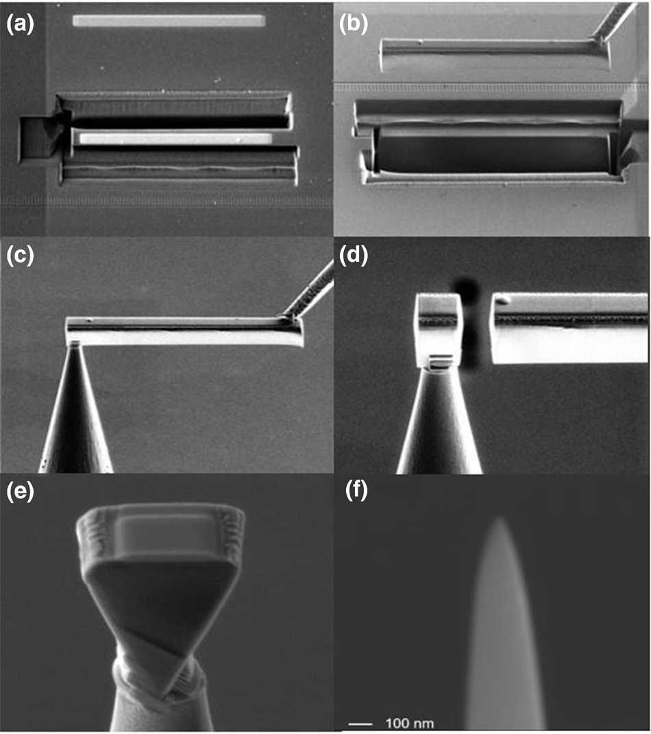
Specimen preparation is the most critical step in APT since the field evaporation of atoms by directly probing the surface of a bulk wafer is not feasible [Reference Tsong78]. The field evaporation and collection of atoms requires the application of a very large electric field (20–40 V/nm) to the sample [Reference Thompson, Lawrence, Larson, Olson, Kelly and Gorman79]. These fields can only be achieved by geometric field enhancement. This field was realized by preparing the specimen apex with a radius of curvature of 50–100 nm for a wide range of materials. Also, the applied field interacts not only with the sharpened tip but also with other features within reasonable proximity (several mm) of the sharpened tip. Therefore, maintaining the electric field required for evaporation requires long, sharp needle-shaped specimens with no material in proximity of the tip [Reference Thompson, Lawrence, Larson, Olson, Kelly and Gorman79]. The requirement for most of the APT specimen is similar to a certain degree for all the material system: (i) the specimen should be sharp with an end radius of ~100 nm to allow field evaporation, (ii) it should be mechanically robust to sustain the evaporation process under high electric field, and (iii) the feature or region of interest must be in the near apex region of the tip so that it lies within the collection of evaporated ions (before the premature rupture of specimen or experiment is aborted) [Reference Kelly and Larson80]. Premature specimen fracture is likely to occur in heterostructure samples as the voltage-induced stress is more likely to exceed the mechanical stability of the tip, especially while passing through the interfaces [Reference Yoon, Seidman, Antoine and Bauer81, Reference Rachbauer, Massl, Stergar, Felfer and Mayrhofer82]. Focused ion beam (FIB)-based lift-out and annular milling was performed as outlined by Larson et al. [Reference Larson, Prosa, Ulfig, Geiser and Kelly57, Reference Larson, Camus, Vargas, Kelly and Miller75, Reference Larson, Petford-Long, Cerezo, Smith, Foord and Anthony83, Reference Larson, Cerezo, Juraszek, Hono and Schmitz84] for sample preparation. This method is most widely used for APT specimen preparation, especially, when multilayer semiconductor materials are involved [Reference Kelly and Larson85]. Prior to the APT specimen preparation, a Ni cap layer of ~50 nm was deposited over all the (AlxGa1−x)2O3 films to protect them from Ga induced surface damages and contaminations. The steps of the site-specific specimen preparation are illustrated in Fig. 2. Trenches were milled in three sides around the area of interest protected by Pt capping as shown in Fig. 2(a). The wedge was removed from the wafer by attaching a micromanipulator to the already cut and free left end of the wedge with subsequent cutting of the wedge from the right end that was attached to the bulk wafer as illustrated in Fig. 2(b). The lifted-out wedge was adjoined on a Si micro-post by Pt deposition as shown in Fig. 2(c). The wedge is then cut free from the micro-post by ion beam milling [Fig. 2(d)], and rest of the wedge attached to the micromanipulator was transferred to other empty Si posts. Pt was deposited on the opposite sides of the wedge-Si post interfaces [Fig. 2(e)]. Sharpening of the mounted post was performed by annular milling followed by 2 kV Ga ion beam cleaning resulting in the needle-shaped APT specimen as shown in Fig. 2(f). Most of the protective Ni cap layers that were deposited before starting the specimen preparations were removed during the 2 kV sharpening process, and only ~5 nm of the Ni layer at the top of the needle was left intentionally. This remaining Ni layer provided the time required for the optimization of the APT experiment condition prior to the acquisition of ions from the (AlxGa1−x)2O3 layers begin. These protective Ni layers were excluded during the 3D atomic reconstructions (the "3D atomic reconstruction of the original specimen and subsequent data analysis" section) and data analysis (the "Results section).
Methodologies of APT specimen preparation from the bulk substrate to final needle-shaped (AlxGa1−x)2O3 films step by step using FIB-based nanofabrication.
Data acquisition
The data acquisition from the specimens is conducted by the field evaporation of ions from the specimen surface [Reference Madireddy, Chung, Loeffler, Sankaranarayanan, Seidman, Balaprakash and Heinonen70]. Figure 3 shows a schematic of the operating principle of APT. In the data acquisition stage, the atoms are sequentially extracted from the needle-shaped surface by controlled field evaporation. This field evaporation is initiated by first ionizing the surface atoms under an intense electrostatic field and then emitting the ions from the tip apex by applying ultrafast laser pulses (355 nm wavelength ultraviolet laser equipped in a CAMECA LEAP 5000 XR atom probe system [Reference Peng, Vurpillot, Choi, Li, Raabe and Gault86]). Since wide bandgap semiconductor tips may exhibit poor response to laser pulsing, it is critical to optimize the APT experimental conditions, especially the base specimen temperature and pulse energy beforehand [Reference Kelly and Larson80]. Experimental parameters including temperature (K), pulse repetition rate (kHz), laser pulse energy (pJ), and evaporation rate (ions per pulse) were optimized to ensure efficient data acquisition from (AlxGa1−x)2O3 tips containing layered structure with varying Al content [Reference Bhuiyan, Feng, Johnson, Huang, Sarker, Zhu, Karim, Mazumder, Hwang and Zhao28, Reference Sarker, Broderick, Bhuiyan, Feng, Zhao and Mazumder29, Reference Mazumder, Sarker, Zhang, Johnson, Zhu, Rajan and Hwang87, Reference Sarker, Zhang, Zhu, Rajan, Hwang and Mazumder88]. The evaporated ions from individual layers are projected and collected in a position-sensitive detector (PSD) that provides the TOF and detection event in 2D positions [Reference Gault, Moody, Cairney and Ringer89] which is used in the reconstruction of the 3D tip image and data analysis.
Schematic presentation of APT operating principle; the field evaporated atoms from the specimen surface by laser pulsing are collected on PSD. PSD records the TOF and position of impact for each and every detected atom.

3D atomic reconstruction of the original specimen and subsequent data analysis
CAMECA's Integrated Visualization and Analysis Software (IVAS 3.8.5a34) was used for the tip reconstruction of the collected APT data. The TOF of all collected ions is transformed into the mass-to-charge state ratio (m/n) which resolves into the mass spectrum [Reference Larson, Prosa, Ulfig, Geiser and Kelly57]. The quality and accuracy of the data is enhanced by background correction of the mass spectrum [Reference Larson, Prosa, Ulfig, Geiser and Kelly57, Reference Gault, Moody, Cairney and Ringer89]. The 3D atom maps of the probed regions were reconstructed in IVAS by following the tip profile method from high magnification SEM images of the tips [Reference Larson, Prosa, Ulfig, Geiser and Kelly57]. IVAS and MATLAB were used for data analysis (structural chemistry of (AlxGa1−x)2O3 films). Due to large amount of ions collected in APT, some material features are suppressed or remain as “concealed” within the massive data set [Reference Broderick, Bryden, Suram and Rajan71]. The advanced data mining strategy was employed to train unprocessed APT data and extract hidden patterns in data to predict material properties such as phase transformation.
Results
Phase transformations of (AlxGa1−x)2O3
The change in the atomic-level structure and chemical composition of (AlxGa1−x)2O3 at Al content, x > 0.25, results in a degraded crystallinity of the films [Reference Bhuiyan, Feng, Johnson, Huang, Sarker, Zhu, Karim, Mazumder, Hwang and Zhao28, Reference Sarker, Broderick, Bhuiyan, Feng, Zhao and Mazumder29, Reference Mazumder, Sarker, Zhang, Johnson, Zhu, Rajan and Hwang87, Reference Sarker, Zhang, Zhu, Rajan, Hwang and Mazumder88] limiting the solubility of α-Al2O3 in β-Ga2O3. This crystal degradation was attributed to the phase separations in (AlxGa1−x)2O3 at high Al content [Reference Krueger, Dandeneau, Nelson, Dunham, Ohuchi and Olmstead10, Reference Kranert, Jenderka, Lenzner, Lorenz, von Wenckstern, Schmidt-Grund and Grundmann26, Reference Bhuiyan, Feng, Johnson, Huang, Sarker, Zhu, Karim, Mazumder, Hwang and Zhao28, Reference Sarker, Broderick, Bhuiyan, Feng, Zhao and Mazumder29, Reference Oshima, Okuno, Arai, Kobayashi and Fujita30]. Since the phase purity is related to film's homogeneity with well-defined Al/Ga stoichiometry at the atomic level, it is required to study the change in the atomic-level structure and chemistry of (AlxGa1−x)2O3 with Al to conclusively determine the Al solubility limit in this alloy. Theoretical studies suggested that elemental segregations are introduced within alloys during phase transformations [Reference Frolov, Asta and Mishin90, Reference Kumara, Balachandramurthi, Goel, Hanning and Moverare91]. APT is capable of providing information about such phase transformations by mapping atomic-scale compositional variations within the materials by revealing the presence of local segregations or inhomogeneity associated with different chemical phases [Reference Guo, Garfinkel, Tucker, Haley, Young and Poplawsky92, Reference Shariq and Mattern93, Reference Devaraj, Gu, Colby, Yan, Wang, Zheng, Xiao, Genc, Zhang, Belharouak, Wang, Amine and Thevuthasan94]. Very recently, APT was employed to investigate the corresponding change of the atomic-level structural chemistry of (AlxGa1−x)2O3 with Al content to observe phase transformation of this alloy [Reference Mazumder, Sarker, Zhang, Johnson, Zhu, Rajan and Hwang87, Reference Sarker, Zhang, Zhu, Rajan, Hwang and Mazumder88].
Two different (AlxGa1−x)2O3 structures with Al content, x = 0.20 and 0.50, were investigated for comparing their structural chemistry. The details of the materials’ structures are reported in Ref. [Reference Mazumder, Sarker, Zhang, Johnson, Zhu, Rajan and Hwang87]. A volume of 50 nm × 50 nm × 4 nm region was extracted from the bulk region of both (Al0.20Ga0.80)2O3 and (Al0.50Ga0.50)2O3 films to investigate the homogeneity of the films in terms of elemental distribution as shown in Figs. 4(a) and 4(d), respectively. Figure 4(b) depicts the local Al distribution along the lateral XY plane in the (Al0.20Ga0.80)2O3 films. Almost homogeneous Al distribution is observed with only 1–2 at.% fluctuations in Al composition. No significant Al segregation was observed, suggesting desired stoichiometry was maintained. The film homogeneity was confirmed via the statistical frequency distribution analysis (FDA) method as shown in Fig. 4(c). In FDA, if the observed elemental distribution resembles with a binomial fitting, this would suggest a homogeneous elemental distribution, while the deviation of the observed distribution from the binomial fitting would indicate statistically significant elemental segregations [Reference Devaraj, Gu, Colby, Yan, Wang, Zheng, Xiao, Genc, Zhang, Belharouak, Wang, Amine and Thevuthasan94]. For (Al0.20Ga0.80)2O3 films, the observed frequency count of Al is fitting with the random binomial distribution, suggesting homogeneous (AlxGa1−x)2O3 layers. A similar compositional analysis was performed in the bulk region of the (Al0.5Ga0.5)2O3 layer. The lateral Al distribution shows severe fluctuations of 10–12 at.% in Al composition identified by the Al-segregated regions (~25 at.% Al) and Al-depleted (~15 at.%) regions as shown in Fig. 4(e). The subsequent FDA analysis of Al distribution in Fig. 4(f) shows a significant deviation from the randomness, suggesting the inhomogeneous (Al0.5Ga0.5)2O3 layer. The reported Pearson coefficient (μ) was 0.8 with a P-value of <0.0001. This high Pearson coefficient with low P-value confirms that a statistically significant amount of segregation is present in the layer with a 95% confidence level during the null hypothesis testing. These results indicate that, at high Al content (x = 0.50), the film homogeneity and stoichiometry are not maintained.
(a) Schematic of the (Al0.2Ga0.8)2O3/Ga2O3 structure with a black box region showing the volume extracted for analysis, (b) lateral Al distribution within the bulk of the (Al0.2Ga0.8)2O3 layer, (c) FDA analysis of Al distribution in (Al0.2Ga0.8)2O3 (Pearson coefficient, μ = 0.1, P-value = 0.2), (d) schematic of the (Al0.5Ga0.5)2O3/Ga2O3 structure with a black box region showing the volume extracted for analysis, (e) lateral Al distribution within the bulk of the (Al0.5Ga0.5)2O3 layer, and (f) FDA analysis of Al distribution in (Al0.5Ga0.5)2O3 (Pearson coefficient, μ = 0.8, P-value <0.001). Reprinted with permission from Ref. [Reference Mazumder, Sarker, Zhang, Johnson, Zhu, Rajan and Hwang87] with the permission of AIP Publishing.

This stoichiometric deviation at high Al content was inferred to appear from the presence of different chemical phases. This was confirmed by comparing APT results with TEM and nano-diffraction patterns as shown in Fig. 5. Figure 5(a) shows the lateral distribution of Al/Ga ratio. Existence of Al-rich and Ga-rich regions are observed throughout the plane resulting from the deviations in expected 50:50 ratios of Al and Ga. These Al-rich and Al-depleted regions imply different chemical phases in the (Al0.5Ga0.5)2O3 layers. The variation in chemical phases was confirmed by high-angle annular dark-field scanning electron microscopy (HAADF STEM) imaging of the (Al0.5Ga0.5)2O3/β-Ga2O3 structure as shown in Fig. 5(b). The (010) β-Ga2O3 substrate shows uniform color contrast, suggesting the homogeneous layer while a contrast variation is observed in (Al0.5Ga0.5)2O3 resulting from chemical segregation (inhomogeneity) in this layer. This indicates the presence of different chemical phases within the (Al0.5Ga0.5)2O3 layer. Phase segregation of this (Al0.5Ga0.5)2O3 film was studied by the nano-diffraction pattern with respect to the (010) β-Ga2O3 substrate. The nano-diffraction pattern of the pure monoclinic β-Ga2O3 substrate is shown in Fig. 5(c). The nano-diffraction pattern for (Al0.5Ga0.5)2O3 in Fig. 5(d) displays additional spots which were not present in pure monoclinic β-Ga2O3 in Fig. 5(c). This suggests that an additional phase is present in (Al0.5Ga0.5)2O3 which can be correlated to the chemical segregations observed in this layer. This study reveals that chemical heterogeneity observed in APT can be attributed to phase segregations in wide bandgap alloys. Such compositional heterogeneity that leads to the phase segregations in (AlxGa1−x)2O3 may be attributed to the different surface mobilities of Al and Ga adatoms [Reference Mazumder, Sarker, Zhang, Johnson, Zhu, Rajan and Hwang87]. Ga atoms with higher adatom mobility can easily drift and are distributed uniformly on the surface, while Al atoms with low surface mobility tend to develop segregated regions that potentially contribute to the observed compositional fluctuations [Reference Mazumder, Sarker, Zhang, Johnson, Zhu, Rajan and Hwang87, Reference Sarker, Zhang, Zhu, Rajan, Hwang and Mazumder88].
(a) Al/Ga composition ratio in bulk (Al0.5Ga0.5)2O3 films and (b) HAADF STEM image of the (Al0.5Ga0.5)2O3/β-Ga2O3 structure, the intensity line profile across the white arrow (inset). Nano-diffraction patterns (probe size = 1 nm) from (c) β-Ga2O3 and (d) (Al0.5Ga0.5)2O3 shown in (b). Reprinted with permission from Ref. [Reference Mazumder, Sarker, Zhang, Johnson, Zhu, Rajan and Hwang87] with the permission of AIP Publishing.

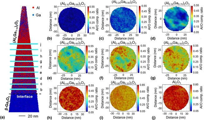
Since APT is capable of providing the most accurate information about phase transformations with varying alloy content, a systematic study was conducted to determine the phase transformations in (AlxGa1−x)2O3 for a wide Al content range of x = 0.1–1.0 [Reference Bhuiyan, Feng, Johnson, Huang, Sarker, Zhu, Karim, Mazumder, Hwang and Zhao28]. The analyzed structures are depicted in Fig. 6, and details about this structure is reported in Ref. [Reference Anhar Uddin Bhuiyan, Feng, Johnson, Chen, Huang, Hwang and Zhao38]. Figure 6(a) shows the schematic of the (AlxGa1−x)2O3 layered heterostructure grown on β-Ga2O3 substrates where Al composition was varied from 10 to 100% with a thickness of 20 nm for each layer. Figure 6(b) shows the Al/Ga ratio along the growth showing the stoichiometry was maintained and the grown (AlxGa1−x)2O3 is ideal for studying the phase transformation.
(a) Schematic diagram of the (AlxGa1−x)2O3 heterostructure with Al content x = 0.10–1.0 and (b) Al/Ga ratio along the growth showing precisely controlled stoichiometry [Reference Sarker, Broderick, Bhuiyan, Feng, Zhao and Mazumder29].

Figure 7(a) shows the reconstructed 3D atom map with red and blue dots representing Al and Ga atoms, respectively. The change in the density of red and blue dots indicates the change in alloy chemistry along the growth. Due to the large number of ions collected, it is difficult to discriminate each (AlxGa1−x)2O3 layer with different Al composition. The lateral chemistry in each layer was investigated by plotting the lateral Al/O ratio as shown in Figs. 7(b)–7(j). For this, 4-nm-thick volumes from the bulk region of each (AlxGa1−x)2O3 layers were extracted to eliminate interfacial effects (adatoms diffusion from top or bottom layers) as explained in Fig. 7(a). At low Al content (x = 10–20%), a nearly homogeneous distribution was observed as shown in Figs. 7(b) and 7(c). This elemental homogeneity is an indication of single-phase stable crystalline (AlxGa1−x)2O3 films. Within this Al content range, the (AlxGa1−x)2O3 films are single monoclinic β-phase stable [Reference Krueger, Dandeneau, Nelson, Dunham, Ohuchi and Olmstead10, Reference Zhang, Saito, Tanaka, Nishio, Arita and Guo12, Reference Ito, Kaneko and Fujita23, Reference Kranert, Jenderka, Lenzner, Lorenz, von Wenckstern, Schmidt-Grund and Grundmann26, Reference Oshima, Okuno, Arai, Kobayashi and Fujita30, Reference Kaun, Wu and Speck33, Reference Vogt, Mauze, Wu, Bonef and Speck95, Reference Li, Chen, Ma, Cui, Ren, Gu, Zhang, Zheng, Ringer, Fu, Tan, Jagadish and Ye96]. As the Al content increases, severely Al-segregated regions appear, as shown in Figs. 7(d)–7(g), suggesting degraded crystallinity due to the co-existence of different chemical phases of (AlxGa1−x)2O3 films within this Al content range. When the Al content is even higher (x = 0.60–1.0), the elemental heterogeneity starts decreasing and homogeneous Al/O distribution is observed as illustrated in Figs. 7(h)–7(j). This regained homogeneity in Al/O distribution with increasing Al content is an indication of the formation of new crystalline α, γ, or η-phase [Reference Krueger, Dandeneau, Nelson, Dunham, Ohuchi and Olmstead10, Reference Kranert, Jenderka, Lenzner, Lorenz, von Wenckstern, Schmidt-Grund and Grundmann26, Reference Wakabayashi, Oshima, Hattori, Sasaki, Masui, Kuramata, Yamakoshi, Yoshimatsu and Ohtomo27, Reference Bhuiyan, Feng, Johnson, Huang, Sarker, Zhu, Karim, Mazumder, Hwang and Zhao28]. The corresponding FDA plots (with bin size = 300 atoms) for Al distribution to statistically quantify the layer's homogeneity are shown in Fig. 8. From the FDA results, it is obvious that, at low Al content of x = 0.10–0.20, the observed Al distribution almost aligns with the random binomial fitting with low value of Pearson coefficient (μ). This suggests homogeneous Al distribution in these layers. The FDA for layers with x = 0.30–0.50 demonstrates the extent of deviations in observed Al distribution from the binomial fitting with high value of Pearson coefficient. This confirms statistically significant elemental segregation within these layers indicating degraded crystallinity resulting from different chemical phases. However, when the Al content increases further (x = 0.60–1.0), the observed Al distribution coincides with that of the binomial distribution followed by low values of Pearson coefficient. This suggests that homogeneous Al distribution throughout the lateral planes is achieved again indicating regained crystallinity. XRD was performed to identify the phases present in the (AlxGa1−x)2O3 films with different Al compositions [Reference Bhuiyan, Feng, Johnson, Huang, Sarker, Zhu, Karim, Mazumder, Hwang and Zhao28]. The XRD peaks were identified as β-phase stable (AlxGa1−x)2O3 films at low Al content (x = 0.10–0.20), while the XRD peaks were attributed to γ-phase (AlxGa1−x)2O3 at high Al contents (x > 0.50) with the co-existence of mixed (β+γ)-phase when the Al content, x is in between (x = 0.20–0.50).
(a) Reconstructed atom map of the (AlxGa1−x)2O3 layered heterostructure with Al composition varying from x = 10–100%, only Al and Ga atoms are shown by red and blue dots, respectively; Lateral distribution Al/O concentration ratio in each layer with the Al composition of (b) x = 0.10, (c) x = 0.20, (d) x = 0.30, (e) x = 0.40, (f) x = 0.45, (g) x = 0.50, (h) x = 0.60, (i) x = 0.80, and (j) x = 1.0. Reprinted with permission from Ref. [Reference Sarker, Broderick, Bhuiyan, Feng, Zhao and Mazumder29] with the permission of AIP Publishing.

FDA of each layer with Al concentration: (a) x = 0.10, (b) x = 0.20, (c) x = 0.30, (d) x = 0.40, (e) x = 0.45, (f) x = 0.50, (g) x = 0.60, (h) x = 0.80, and (i) x = 1.0 [Reference Bhuiyan, Feng, Johnson, Huang, Sarker, Zhu, Karim, Mazumder, Hwang and Zhao28].

Machine learning in APT to study phase transformation of (AlxGa1−x)2O3
Supporting characterization tools (STEM, nano-diffraction, and XRD) were required to confirm if the (AlxGa1−x)2O3 film inhomogeneity or elemental (Al) segregation revealed by APT were indicative of phase transformations due to varying Al content. The reason is, some material features (phase transition for example) remain as “latent” within the huge amount of data (ions) collected in APT [Reference Broderick, Bryden, Suram and Rajan71, Reference Peng, Lu, Hatzoglou and da Silva97]. Very recently, an unsupervised machine learning approach, principal component analysis (PCA), has been applied to APT data to enable the extraction of patterns from the unprocessed data set to capture material's phase-related information, which usually remains as hidden due to high dimensionality of the data [Reference Sarker, Broderick, Bhuiyan, Feng, Zhao and Mazumder29]. PCA reduces the data dimensionality by transforming multi-component quantities of directionally correlated variable sets into a linearly uncorrelated variable set and still preserving most of the information [Reference Peng, Lu, Hatzoglou and da Silva97]. These transformed linearly uncorrelated variable sets are the principal components (PCs) in the dimensionally reduced data set. PCA generates principal alignment directions on the basis of how much variance in the data is captured. The variance of material features such as alloy composition variation captured by these PCs is interpreted and correlated to the corresponding material properties like phase transitions [Reference Mejía-Uriarte, Sato-Berru, Navarrete, Kolokoltsev and Saniger98]. In PCA analysis, principal component 1 (or PC1) represents the direction of a variable that is mostly affecting the data, while PC2 is the factor which is the second highest in terms of variance. PCA was performed on the TOFs of ions of (AlxGa1−x)2O3 with x = 0.10–1.0. The TOF for any specific element being constant due to a fixed value of the corresponding mass-to-charge state ratio, the shape of the TOF peaks should retain the similar shape except the peak intensity which would be subjected to change due to the change in the alloy composition. This variation of TOF peaks will not be visible from the TOF spectrum of the entire heterostructure while this peaks shape deviation can be observed when the entire spectrum is sampled equally as shown in Figs. 9(a)–9(k). The differences in TOF peak shapes and intensities of one sampled spectrum compared with next or previously sampled spectra are arising from the change in the alloy composition. These equally sampled spectra were provided as input to the PCA to extract hidden patterns in these peak deviations to explore phase-related information. The initial processing of the APT TOF data and the algorithm used for the data dimensionality reduction using PCA are described by the flowchart as shown in Fig. 10. Figure 11 shows the PCA result where PC1 is capturing the change in alloy chemistry (Al/Ga ratio) along with the growth which is the largest factor affecting the data, while PC2 is reflecting the TOF peak changes, which is the second most influential factor. From the PC1 versus PC2, a linearly increasing trend up to x ≤ 0.30 is observed, this positive correlation between the variation of alloy composition and peak shapes. This increasing trend was attributed to degrading crystallinity. Positive correlation up to x ≤ 0.30 in PC1 versus PC2 suggests that up until this alloy composition, (AlxGa1−x)2O3, the single-phase crystalline structure is retained. As mentioned earlier, within this Al composition range, the (AlxGa1−x)2O3 films are β-phase stable. When x ≥ 0.30 and x ≤ 0.50, no trend is observed within Al/Ga ratio and TOF peak changes indicating PC1 and PC2 are negatively correlated. This suggests that the presence of a degraded crystallinity within this Al content range. When Al content, x > 0.50, a linearly decreasing trend is observed between PC1 and PC2. The retention of this linear trend for x = 0.60–1.0 is suggesting that the Al/Ga variation is positively correlated with the TOF peak deviations, while the decreasing value of PC1-PC2 implies the crystallinity is being restored as Al composition is increasing. This result indicates a new crystalline phase formed. From the XRD result, in this Al content range (x = 0.6–1.0), the (AlxGa1−x)2O3 films are γ-phase stable. Thus, combining APT with the data mining strategy, phase transformation is determined without any supporting tool like STEM or nano-diffraction. This study demonstrates that the capability of APT can be extended to investigate not only the structural chemistry of materials but also information about phase transformation can be obtained.
(a–k) Equal sampling of the TOF spectrum for the (AlxGa1−x)2O3 films with x = 0.10–1.0 by sectioning into equal volumes. The typical output of APT is an image showing atom positions having a single TOF spectrum for the whole data set. The first step is to divide the sample into multiple sections, and each section will have a respective TOF spectrum as shown in (b–k). Reprinted from Ref. [Reference Sarker, Broderick, Bhuiyan, Feng, Zhao and Mazumder29] with the permission of AIP Publishing.

The flow chart illustrating the algorithm used to perform PCA on the TOF of (AlxGa1−x)2O3 films with x = 0.1–1.0. Reprinted from Ref. [Reference Sarker, Broderick, Bhuiyan, Feng, Zhao and Mazumder29] with the permission of AIP Publishing.

PCA showing phase transition in (AlxGa1−x)2O3 with x = 0.10–1. Reprinted from Ref. [Reference Sarker, Broderick, Bhuiyan, Feng, Zhao and Mazumder29] with the permission of AIP Publishing.

Doping interaction in (AlxGa1−x)2O3 by APT
Dopant detection and dopant profile analysis
Extrinsic n-type doping is required to achieve high conductivity in (AlxGa1−x)2O3 since the intrinsic oxygen vacancies do not contribute in conduction [Reference Dong, Jia, Xin, Peng and Zhang35, Reference Hassa, Wenckstern, Vines and Grundmann37]. To realize desired conductivity, it is critical to address the issue with donor compensation [Reference Götz, Johnson, Chen, Liu, Kuo and Imler39, Reference Uedono, Tenjinbayashi, Tsutsui, Shimahara, Miyake, Hiramatsu, Oshima, Suzuki and Ishibashi40, Reference Chichibu, Miyake, Ishikawa, Tashiro, Ohtomo, Furusawa, Hazu, Hiramatsu and Uedono41, Reference Gogova, Wagner, Baldini, Schmidbauer, Irmscher, Schewski, Galazka, Albrecht and Fornari42, Reference Zhang, Farzana, Arehart and Ringel43, Reference Chichibu, Iwai, Nakahara, Matsumoto, Higuchi, Wei and Tanigawa44] that leads to a low carrier mobility at high doping level and adversely affects the electrical and optical properties of the devices [Reference Harris, Baker, Gaddy, Bryan, Bryan, Mirrielees, Reddy, Collazo, Sitar and Irving99]. The mechanism of this dopant compensation effect is still under debate. Some studies proposed that n-type dopants involve in the formation of DX transition centers that attributes to the self-compensation of donors [Reference Park and Chadi100, Reference McCluskey, Johnson, Van de Walle, Bour, Kneissl and Walukiewicz101, Reference Gordon, Lyons, Janotti and Van de Walle102]. A DX transition center occurs when a donor impurity captures two electrons and undergoes a large lattice relaxation to transform into an acceptor, resulting in fewer electrons available for conduction. Another factor that is accounted for compensating knee is the material defects [Reference Harris, Baker, Gaddy, Bryan, Bryan, Mirrielees, Reddy, Collazo, Sitar and Irving99]. The formation of native defects such as cation vacancies (like Ga vacancy, VGa or Al vacancy, VAl) associated with impurity doping can be electrically favorable and tend to diffuse toward the active bulk region [Reference Chichibu, Miyake, Ishikawa, Tashiro, Ohtomo, Furusawa, Hazu, Hiramatsu and Uedono41]. The interaction of n-type dopants with these native defects (VGa and VAl) results in the formation of n-type dopant interstitial-III site vacancy defect complexes (VGa-SiGa or VAl-SiAl for example) that act as charge trapping centers. This leads to the compensating knee in wide bandgap semiconductors like GaAs, GaN, AlGaN, and Ga2O3 [Reference Uedono, Tenjinbayashi, Tsutsui, Shimahara, Miyake, Hiramatsu, Oshima, Suzuki and Ishibashi40, Reference Zhang, Farzana, Arehart and Ringel43, Reference Chichibu, Iwai, Nakahara, Matsumoto, Higuchi, Wei and Tanigawa44, Reference Harris, Baker, Gaddy, Bryan, Bryan, Mirrielees, Reddy, Collazo, Sitar and Irving99, Reference Farzana, Ahmadi, Speck, Arehart and Ringel103]. N-type doping is found to be particularly challenging in the wide bandgap alloys when the alloy composition is varied [Reference Varley, Perron, Lordi, Wickramaratne and Lyons36]. In AlxGa1−xN, it has been observed that n-type doping at x > 0.70 is very challenging because of the drastic increase of dopant activation energy followed by carrier compensation due to deep level defects and deep Si DX centers [Reference Nakarmi, Kim, Zhu, Lin and Jiang104, Reference Borisov, Kuryatkov, Kudryavtsev, Asomoza, Nikishin, Song, Holtz and Temkin105, Reference Collazo, Mita, Xie, Rice, Tweedie, Dalmau and Sitar106]. In Ge doped AlGaN, dopant atoms are observed to form clusters at high Al content which was attributed to the increase in smaller Al–N bonds compared with larger Ga–N and Ge–N bonds [Reference Blasco, Ajay, Robin, Bougerol, Lorentz, Alves, Mouton, Amichi, Grenier and Monroy107]. (AlxGa1−x)2O3 being a similar class of material system, these above-stated issues may impose difficulties in achieving the desired doping profile. The n-type doping in (AlxGa1−x)2O3 is theoretically investigated with group IV elements (C, Si, Sn, and Ge) and transition metals (Hf, Zr, and Ta) as they are predicted to substitute on cation sites [Reference Varley, Perron, Lordi, Wickramaratne and Lyons36]. Si was found to be the most suitable dopant as it remains a shallow level donor even at the highest Al content while other dopants become deep level donor at high Al. Experimental demonstration of Si doping in (AlxGa1−x)2O3 is also reported where Si incorporation was confirmed [Reference Hassa, Wenckstern, Vines and Grundmann37, Reference Anhar Uddin Bhuiyan, Feng, Johnson, Chen, Huang, Hwang and Zhao38, Reference Ranga, Rishinaramangalam, Varley, Bhattacharyya, Feezell and Krishnamoorthy108, Reference Ranga, Bhattacharyya, Rishinaramangalam, Ooi, Scarpulla, Feezell and Krishnamoorthy109], but comprehensive understanding of the atomic-level dopant behavior with the doped (AlxGa1−x)2O3 films needs further effort. To characterize the n-type doping in (AlxGa1−x)2O3 with varying Al content, it is extremely important to accurately detect and quantify the dopant elements. Also, a firm knowledge is required about how the dopant atoms are interacting with the matrix, especially, when the alloy composition is varied.
APT has already demonstrated its outstanding capability in characterizing dopants profile in other semiconductor systems having complex 3D geometry and complex alloy chemistry [Reference Ronsheim, Hatzistergos and Jin110, Reference Du, Burgess, Gault, Gao, Bao, Li, Cui, Yeoh, Liu, Yao, Ceguerra, Tan, Jagadish, Ringer and Zheng111, Reference Yeoh, Hung, Chen, Lin and Lee112]. Inspired from these results, Si doped (AlxGa1−x)2O3 with x = 0–1.0 was investigated by APT [Reference Sarker, Bhuiyan, Feng, Zhao and Mazumder113]. The Si dopant incorporation was confirmed from the APT mass spectrum where Si peaks for both Si1+ at 28 Da and Si2+ at 14 Da were distinctly identified as shown in Fig. 12. The dopant concentration for Si in each (AlxGa1−x)2O3 layer was measured and found to be in the range of 1–7 × 1018 cm−3, which was as estimated from the growth (~5 × 1018 cm−3). No peak overlap with the thermal tail from Al1+ and Al2+ was observed to introduce quantification artifacts, thanks to the optimization of laser pulse energy and base temperature. This implies successful dopant incorporation in each (AlxGa1−x)2O3 layer regardless of the alloy compositions.
(a) APT mass spectrum (background corrected) of Si doped (AlxGa1−x)2O3 with x = 0–100%; (b) magnified mass spectrum from the dotted region in (a) showing Si peaks at 14 Da associated with Si2+ and (c) at 28 Da associated to Si1+. No peak overlap from tails from Al was observed [Reference Sarker, Bhuiyan, Feng, Zhao and Mazumder113].

To investigate the dopant distribution whether it is homogeneous or non-homogeneous, statistical FDA from individual alloy composition was performed. Figure 13 reports the FDA of Si distribution from alloy volume of 4 nm thickness, extracted from the bulk of each layer. In all cases, the observed Si distribution closely resembles the binomial fitting with the low value of Pearson coefficient (μ) while a μ value close to 1 would indicate the presence of segregation [Reference Devaraj, Gu, Colby, Yan, Wang, Zheng, Xiao, Genc, Zhang, Belharouak, Wang, Amine and Thevuthasan94]. The FDA results suggest dopant distribution in each (AlxGa1−x)2O3 is close to homogeneous and efficient n-type doping was achieved in (AlxGa1−x)2O3 over the whole alloy composition range.
FDA of Si distribution in each layer with Al composition of (b) x = 0.0, (c) x = 0.10, (d) x = 0.20, (e) x = 0.30, (f) x = 0.40, (g) x = 0.50, (h) x = 0.60, (i) x = 0.80, and (j) x = 1.0 [Reference Sarker, Bhuiyan, Feng, Zhao and Mazumder113].

Dopant interaction in (AlxGa1−x)2O3
To explore how dopant Si affects the microstructure of the (AlxGa1−x)2O3 layers with varying alloy composition, the interaction of these dopants with the neighboring atoms of the doped matrix was investigated using radial distribution function (RDF) [Reference Schmidt, Peng, Poplawsky and Weckhuysen114]. RDF is a very efficient statistical analysis technique to examine the affinity between different species located within very short distances [Reference Schmidt, Peng, Poplawsky and Weckhuysen114]. The RDF method was extended to study species interaction with varying alloy compositions. RDF provides the radially outward concentrations starting from each atom of any selected species and returns the probability density of finding an atom j at a distance r given the central atom i [Reference Zhou, Odqvist, Thuvander and Hedström115]. In this case, considering Si as the atom of interest (atom i), the concentration profile of Al and Ga (atom j) starting from each Si atoms in a radially outward direction within small volumes was measured via RDF as illustrated in Fig. 14. RDF determined Ga and Al concentration surrounding each dopant Si atom (considering as the center, distance, d = 0) within a volume of 10 nm × 10 nm × 1 nm taken in the bulk region of each (AlxGa1−x)2O3 layer. At low Al contents (x = 0–0.20), high Ga concentration surrounding the Si atoms (at d = 0) was observed [Figs. 14(a)–14(c)] while low Al concentration suggests, dopant Si is occupying on Ga site. Ga concentration tends to decrease while approaching the location of center Si atoms which suggest the possible presence of Ga vacancy (VGa). Dopant Si may interact with these VGa and form VGa-SiGa defect complex which contributes to compensating knee [Reference Uedono, Tenjinbayashi, Tsutsui, Shimahara, Miyake, Hiramatsu, Oshima, Suzuki and Ishibashi40, Reference Chichibu, Miyake, Ishikawa, Tashiro, Ohtomo, Furusawa, Hazu, Hiramatsu and Uedono41]. For layers with x = 0.30–0.50, the distribution of Ga and Al surrounding the dopant Si is not obvious and Si may substitute in either Ga or Al sites [Figs. 14(d)–14(f)]. This may lead to the formation of VGa-SiGa or VAl-SiAl complex. When the Al content is high (x = 0.60–1.0), the high Al concentration surrounding the dopants implies Al site occupancy [Figs. 14(g)–14(i)] and the dopant compensation would have dominant VAl-SiAl defect complexes [Reference Harris, Baker, Gaddy, Bryan, Bryan, Mirrielees, Reddy, Collazo, Sitar and Irving99]. The information obtained from this analysis was significant in understanding which kind of cationic site n-type dopants would occupy and the type of dominant defects that would be responsible for dopant compensation in (AlxGa1−x)2O3 when Al content is varied.
RDF results in each (AlxGa1−x)2O3 layers showing Si is occupying (a–c) Ga site at (AlxGa1−x)2O3 at x = 0.10–0.20; (d–f) Ga or Al site at (AlxGa1−x)2O3 at x = 0.30–0.50; (g–i) Al site at (AlxGa1−x)2O3 at x = 0.60–0.80 [Reference Sarker, Bhuiyan, Feng, Zhao and Mazumder113].

Conclusion and outlook
As discussed in this review, the versatile capability of APT to investigate the atomic-scale structural chemistry of (AlxGa1−x)2O3 provided unprecedented insight on how phase transformations in this material occur with changing the alloy composition. Complementing APT data with machine learning-based analyses to determine latent features such as phase transformation of (AlxGa1−x)2O3 can change the paradigm of currently adapted experimental approaches to understand similar phenomena not only for ultra-wide bandgap oxides but also any other materials exhibiting these phase-related issues. The characterization of n-type dopant distribution in (AlxGa1−x)2O3, as well as, the knowledge of how this dopant influences the doped material when the alloy composition is being varied, revealed information about the dominant type of defect and dopant-defect complex that would affect chemical and physical properties of (AlxGa1−x)2O3 at different alloy compositions. The structural and compositional information of (AlxGa1−x)2O3 with varying alloy composition and n-type doping provided in this study would be significant for not only the growth community to grow high-quality material allowing efficient doping but also the device engineers and scientists in designing and fabrication of high-performance devices.


 Open access