





Introduction
For short and mid-range high data rate interconnects, dielectric waveguide (DWG) cables can be an interesting alternative to commonly used copper cables or optical fibers [Reference Song, Huxian and Hyeon-Min1]. DWGs are flexible, lightweight, and cost-effective. Moreover, they have low losses ($2 - 3\, {\rm dB}/{\rm m}$ at 100 GHz) and can be designed to reduce their dispersion to values lower than 0.1 ps/GHz/m even over large bandwidths [Reference Meyer, Krüger and Schneider2]. Such a DWG cable consists of a dielectric core that is surrounded by a cladding with a permittivity that is less than the core's permittivity. To ensure low losses, the core consists of a low-loss material like PE or PTFE and the cladding is made of low-loss foam. Due to the fact that the wave not only propagates inside the core but also in the cladding, an additional protective cladding layer is added [Reference De Wit, Zhang and Reynaert3, Reference Distler, Oppelt, Schür and Vossiek4]. To ensure an easy manufacturing process of such a cable, a simple cross-sectional geometry of the DWG core is desirable (e.g. rectangular or circular cross-sections). In recent publications the transmission of linearly polarized waves along dielectric waveguides with these cross-sections has been demonstrated in high data rate links under laboratory conditions [Reference Sawaby, Dolatsha, Grave, Chen and Arbabian5, Reference Van Thienen, Zhang and Reynaert6]. The mode that is excited in the DWG for these applications is the fundamental mode HE11. This hybrid mode exists in two orthogonal polarizations: ${\rm HE}_{11}^x$
 and ${\rm HE}_{11}^y$
 . Under perfect conditions, DWGs with rectangular and circular cross-sections theoretically maintain the linear polarization of a wave traveling along the waveguide. However, the polarization of the transmitted wave can be disturbed by twists or bends of the waveguide. Moreover, in circular cross-sectional waveguides, the linearly polarized wave does not follow the waveguide in case of twists. Therefore, the excitation of the wave at the transmitter and the detection of the wave at the receiver must be in the same orientation to receive maximum power. This is not feasible for practical applications. Hence, a transition between DWG and transceiver is needed that is able to convert the power to or from both polarizations. This can be done either by a circularly or a dual-polarized transition. An advantage of dual-polarized transitions is their ability to excite different waves in both polarizations at the same time. Therefore, in high data rate systems which use DWGs, the data rate could theoretically be doubled by transmitting data in both polarizations simultaneously.
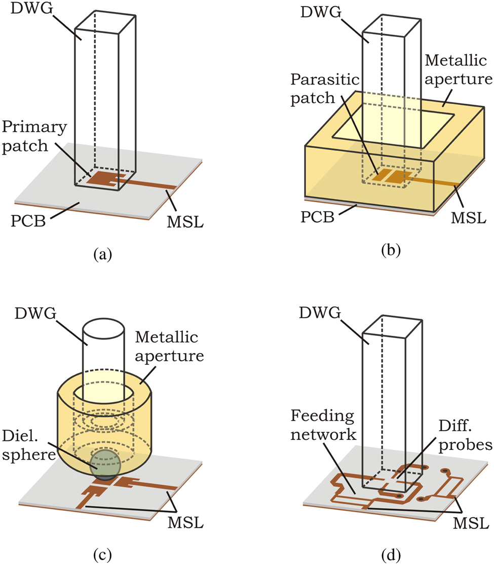
To connect DWGs to commonly available transceiver chips in the mm-wave frequency range, transitions from planar waveguides (e.g. microstrip lines (MSLs)) to DWGs are needed. Linearly polarized transitions were already intensively studied [Reference Distler, Schür and Vossiek7–Reference Häseker and Schneider12]. These transitions can be distinguished into two different types: transitions with horizontal alignment between DWG and printed circuit board (PCB) as well as transitions with vertical alignment. A horizontal alignment between DWG and PCB allows the use of broadband traveling wave structures (e.g. Vivaldi structures) to excite the fundamental mode HE11 in the DWG [Reference Richter, Yazici, Ziegler and Schmidt8–Reference Ocket, Cauwe and Nauwelaers10]. These structures have a large space consumption and the excitation of both polarizations at the same time is difficult [Reference Dolatsha and Arbabian13]. For a transition with the vertical alignment of DWG and PCB, usually resonant structures like patches are used. These structures are compact and the excitation of the second polarization is quite simple. The drawback of these resonant structures is their narrow bandwidth. In [Reference Yu, Liu, Ye, Ren, Liu and Gu11] a simple transition between MSL and DWG using a single microstrip patch has been demonstrated that achieved a relative 10 dB-bandwidth of ${\approx }\,5\percnt$ at 210 GHz (see Fig. 1(a)). To increase the bandwidth, different approaches have been investigated in the recent years. Most of these approaches are using parasitic patches on the PCB that leads to a higher space consumption [Reference Häseker and Schneider12, Reference Dey and Hesselbarth14, Reference Dey and Hesselbarth15]. Furthermore, metallic apertures are added to improve the coupling efficiency into the DWG that increase the complexity and weight of the transitions and impede an integration into a package. Figure 1(b) shows a linearly polarized transition presented in [Reference Häseker and Schneider12] with one parasitic patch and a metallic waveguide aperture. This transition achieved a relative bandwidth of 10% but increases the space consumption on the PCB due to the metallic aperture. To overcome this disadvantage, in [Reference Dey and Hesselbarth14, Reference Dey and Hesselbarth15], a dielectric sphere is used to space apart the metallic structure from the PCB to reduce the contact surface on the PCB and thus enable an integration into a package (see Fig. 1(c)). This approach was presented as linearly and dual-polarized transition but is still bulky and heavy due to the metallic structure added to the sphere. A totally different approach can be seen in Fig. 1(d) [Reference Yu, Ye, Ding, Liu, Xu, Liu and Gu16] where a differential fed probe transition allows broadband and dual-polarized operations. This transition comes without metallic aperture but needs a feeding network that increases space consumption and requires an additional layer.
An overview of recently published transitions from PCB to DWG with vertical alignment: (a) Linearly polarized patch [Reference Yu, Liu, Ye, Ren, Liu and Gu11], (b) Linearly polarized parasitic patch with metallic aperture [Reference Häseker and Schneider12], (c) Dual-polarized parasitic patch with dielectric sphere [Reference Dey and Hesselbarth15], and (d) Dual-polarized probe feed transition with feeding network [Reference Yu, Ye, Ding, Liu, Xu, Liu and Gu16].
In this paper, a dual-polarized broadband transition from MSL to circular DWG using a stacked patch inside the DWG is presented. This transition reduces the space consumption on the PCB and comes without any metallic aperture to reduce the complexity and weight of the transition. The design allows an easy integration into a PCB layout or chip package. One critical parameter in the manufacturing process of such a transition is the positioning of PCB and DWG. A large misalignment of PCB and DWG could dramatically impair the electrical properties of the overall transition. Therefore, an extensive sensitivity analysis is presented that clarifies the acceptable manufacturing tolerances for the transition design. The simulation results are compared to the measurement results of various manufactured prototypes to prove the robustness of the design.
Transition design
The basic concept of the MSL-to-DWG transition uses a circular microstrip patch to excite both perpendicular polarizations of the fundamental mode ${\rm HE}_{11}^x$ and ${\rm HE}_{11}^y$
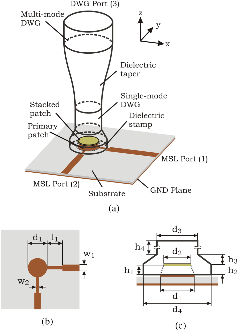
 in a DWG. Just as for patch antennas, the bandwidth and coupling efficiency of a transition using only one MSL patch are mainly limited by the permittivity and thickness of the substrate. Increasing the thickness and/or reducing the permittivity of the substrate increases the bandwidth but might cause surface modes in the substrate. Due to these limitations, such a single patch PCB-to-DWG transition usually achieves a relative 10 dB-bandwidth of roughly 5% [Reference Yu, Liu, Ye, Ren, Liu and Gu11]. To enhance the bandwidth without increasing the space consumption on the PCB, a parasitic patch (hereinafter called “stacked patch”) is centered above the MSL patch (hereinafter called “primary patch”). The stacked patch is fed by the primary patch by electromagnetic coupling. Now the transition's bandwidth is mainly determined by the permittivity and thickness of the material between both patches. The stacked patch is placed on the bottom of a cavity that is drilled into the DWG. The basic concept of the presented PCB-to-DWG transition is shown in Fig. 2(a). The primary patch is fed by two orthogonal MSLs. The MSL in the x-direction excites the ${\rm TM}_{11}^x$
 mode in both patches which in turn excites the fundamental mode ${\rm HE}_{11}^x$
 in the dielectric waveguide. For the second polarization, a second MSL in the y-direction is added to the patch that feeds the ${\rm TM}_{11}^y$
 mode in both patches which in turn excites the ${\rm HE}_{11}^y$
 mode. To match the edge impedances of the primary patch to the characteristic impedance of the MSL (here Z 0 = 50 Ω) an impedance transformer is placed between each MSL and patch.
Schematic structure of the transition between microstrip line and circular dielectric waveguide (a) as well as PCB layout (b) and detailed view of the dielectric structure (c) [Reference Meyer, Karau and Schneider17].
To further increase the coupling efficiency without adding a metallic aperture, it has been found that the diameter of the DWG near the patches has to be larger than the guided wavelength of the fundamental mode HE11 in the DWG (D/λg ≥ 1). Following the cut-off condition for the lowest higher order modes TE01 and TM01 in a circular DWG [Reference Snitzer18], the core diameter D relative to the free space wavelength λ0 has to be

to be a single-mode waveguide. Here, χ0,1 = 2.405 is the first root of the Bessel function of zero order J 0 and ɛr,1 and ɛr,0 are the relative permittivities of the DWG's core and cladding. Since equation (1) can not be fulfilled in case of a high coupling efficiency with available materials, the propagation of higher order modes is possible in this section of the transition. If both patches or DWG and PCB are not perfectly centered, higher order modes will be excited. To suppress these unwanted modes, this multi-mode section (hereinafter called “dielectric stamp”) is followed by a short single-mode section. Such a single-mode section can be realized by either decreasing the permittivity of the material or reducing the diameter (see equation (1)). Here, the single-mode section is realized by changing the diameter. To avoid additional reflections and enhance the radiation of unwanted higher order modes, a taper between dielectric stamp and single-mode section is introduced.
In case of a single-mode DWG cable, the core of this cable can directly be connected to the single-mode section. However, it might be advantageous to use multi-mode DWGs in a high-data rate system in combination with a higher-order-mode filter due to the low waveguide dispersion of certain circular multi-mode designs as stated in [Reference Meyer, Krüger and Schneider2] and [Reference Meyer, Turan and Schneider19]. For this purpose, in our transition, a dielectric taper is added to the single-mode section to adapt the transition to the core diameter of a multi-mode DWG. Similar to the approach presented in [Reference Meyer, Krüger, Obermeyer and Schneider20], a cosine-shaped dielectric taper is used to couple a wave from a single-mode DWG into a multi-mode DWG with negligible higher order mode excitation.
To demonstrate the stacked-patch transition, a design is optimized to connect a 50 Ω MSL on a Rogers 3003 substrate (ɛr = 3.0, h = 0.127 mm) with a multi-mode dielectric waveguide made of HDPE (ɛr = 2.3, tan δ = 1 × 2.2−4) with a diameter of D = 4 mm at W-band frequencies. Especially the frequency range between 80 and 90 GHz is of great interest since commonly available E-band transceivers are operating in this frequency range. The dimensions of the design are shown in Table 1 (Column: Levels “o”). The ability of such a transition to be implemented into a chip package depends on its robustness toward manufacturing tolerances. Therefore, an extensive sensitivity analysis has been performed.
Parameter dimensions with their corresponding tolerance limits

Sensitivity analysis
For the sensitivity analysis, 13 parameters are considered. These parameters are divided into control and noise parameters. Control parameters are dimensions that can be modified during the design process. They contain the dimensions of the dielectric structure and the PCB layout. The taper length l Taper as well as the MSL width w 1 are not taken into account for the sensitivity analysis. Furthermore, parameters that are not part of the design but can occur during the manufacturing process are denoted as noise parameters. In this analysis, we focus on the non-perfect alignment between PCB and dielectric structure. Therefore, the noise parameters contain an x-offset, a y-offset as well as a z-offset which means an air gap between PCB and dielectric structure. The permittivity and thickness of the substrate are assumed to be highly reliable and therefore are not included in this analysis. For each parameter, a lower tolerance limit ( − ) and an upper tolerance limit ( + ) are specified. Combined with the nominal value (o), 3 levels per parameter are obtained (see Table 1). Each tolerance limit depends on the structure the limit belongs to. For dimensions of the PCB, layout limits of ± 10 μm are assumed. The dielectric structure could be fabricated by injection molding, therefore higher tolerances of ± 100 μm are specified for the dimensions of the dielectric structure. For a horizontal misalignment between PCB and dielectric structure, the tolerances are set to ± 100 μm. For the z-offset, a nominal value of 0 μm and two values of + 25 and + 50 μm are specified.
Since the number of parameters k and levels per parameter s of the sensitivity analysis is large, a full factorial experiment would lead to a huge number of trials (s k). To reduce the number of simulations, the Taguchi Method [Reference Taguchi21] is chosen for the sensitivity analysis. The Taguchi Method utilizes orthogonal arrays (OA) to determine the experiment plan for the analysis and reduces the number of simulations drastically by obtaining results close to that of a full factorial experiment [Reference Hedayat, Sloane and Stufken22]. An OA(N, k, s, t) is a matrix with N rows and k columns. Each row in an OA represents one experiment where a certain combination of levels per parameter s is applied. The strength t indicates that an interaction of t parameters is taken into account. The OA ensures equally distributed occurrence of levels for each parameter and each interaction of parameters.
The presented sensitivity analysis combines two orthogonal arrays. This allows to determine the influence of the control parameters on the variance of the electric properties of our design in the presence of the noise factors. The variations of control parameters are determined by an OA 1(27, 10, 3, 2), the variation of the noise parameters by an OA 2(9, 3, 3, 2). For each row in the control parameter OA 1, the scattering parameters (S-parameters) for all rows in the noise parameter OA 2 are simulated using Ansys HFSS. This leads to 27 × 9 = 243 simulations instead of 313 = 1.59 × 10⁶ simulations for a full factorial experiment.
To determine the effect of the control parameters on the sensitivity of the overall transition, a fitness value is calculated that evaluates the relation between average electrical performance and its variance. As fitness value Taguchi introduced the Signal-to-Noise ratio (SNR). The SNR in terms of sensitivity analysis determines the ratio of the squared mean of all variations (signal) and the error power (noise). The SNR i for every experiment i is calculated by
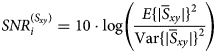
where $\overline {S}_{xy}={E}\lcub \vert {S_{xy}\lpar f\rpar }\vert \rcub$ is the mean absolute value of the S-parameter S xy(f) over all frequencies between 80 and 90 GHz. The following S-parameters S xy(f) are included for the analysis: The transmission coefficient from the MSL port 1 to the wanted polarization ${\rm HE}_{11}^x$
 of the DWG at port 3 ($S_{31}^x$
 ), the unwanted transmission between both MSL ports (port 1 and 2) S 21, referred as isolation as well as the transmission coefficient between the MSL port 1 and the unwanted polarization ${\rm HE}_{11}^y$
 of the DWG ($S_{31}^y$
 ), referred as crosstalk. To determine the impact of each parameter n on the S-parameters, the average $\overline {SNR}\lpar n\comma\; m\rpar$
 of all SNR i values for each parameter n and all levels m is calculated:

Thus, the $\overline {SNR}$ is a measure of the change in electrical properties in case that a parameter changes according to its specified tolerances. Subsequently, a Pareto analysis is performed on the average $\overline {SNR}$
 where the parameters with the highest impact on the electrical properties are identified. The results for the transmission coefficient $S_{31}^x$
 are depicted in Fig. 3(a), for the isolation S 21 in Fig. 3(b) and for the crosstalk $S_{31}^y$
 in Fig. 3(c).
Pareto analysis for the control parameters given in Table 1 of the transmission coefficient $S_{31}^x$ (a), isolation S 21 (b), and crosstalk $S_{31}^y$
 (c).
(c).
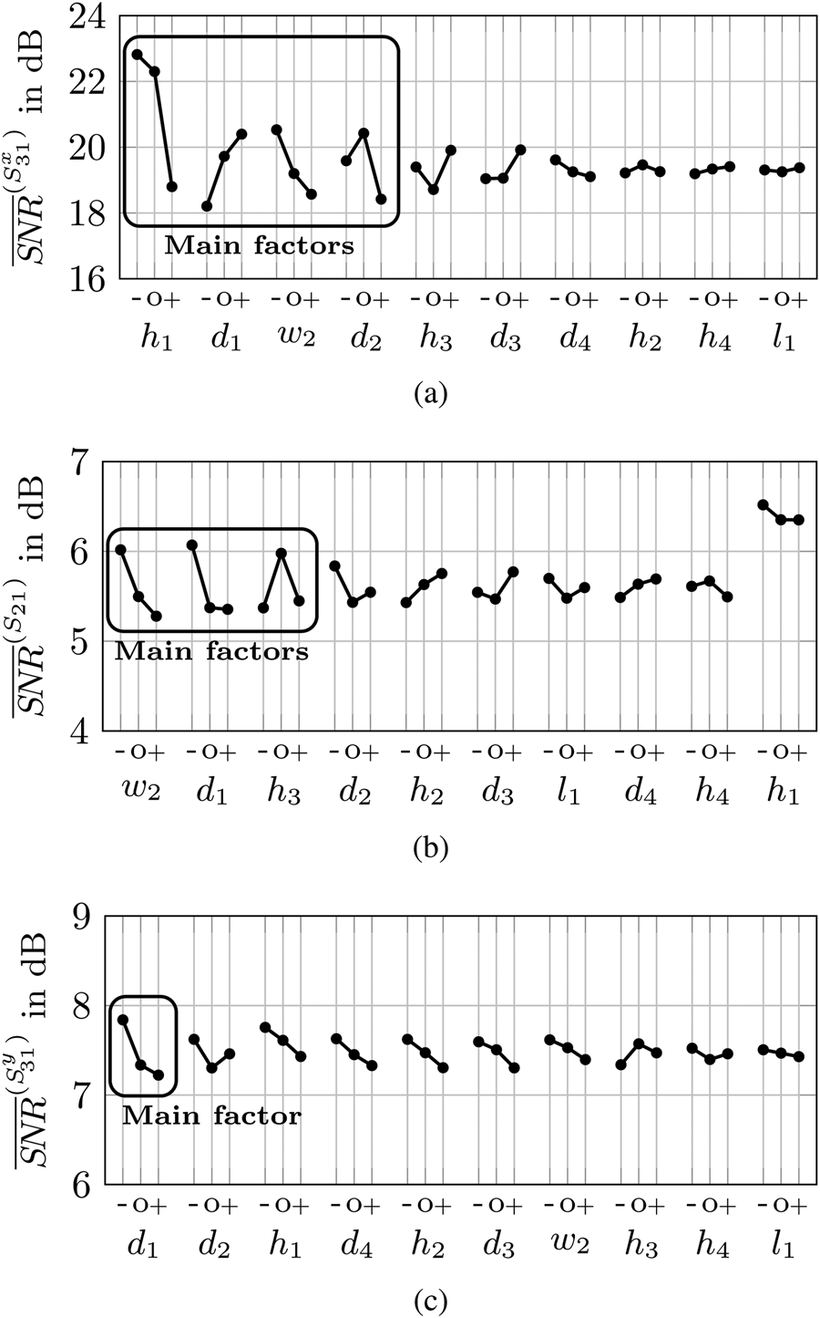
Figure 3(a) identifies four main influencing factors of the transmission coefficient $S_{31}^x$ : The distance between both patches h 1, the diameter of the primary patch d 1, the width of the impedance transformer w 2 as well as the stacked patch diameter d 2. The first main factor, the distance between both patches h 1, already shows a quite high $\overline {SNR}$
 for the nominal value of the design. A larger value of h 1, however, leads to a significantly lower $\overline {SNR}$
 and therefore an increasing variance of the transmission coefficient $S_{31}^x$
 . This can be explained by the one-sided distribution of the tolerance values of the z-offset. With increasing z-offset, the distance between primary and stacked patch also increases. Thus, a tendentially smaller distance between both patches than the nominal value shows a higher robustness against an air gap between PCB and dielectric structure. For isolation and crosstalk, however, the distance h 1 plays a subordinate role. Especially for the isolation, a significantly lower influence can be observed than for all other parameters. The second main factor, the diameter of the primary patch d 1, shows an increasing variance of the transmission coefficient $S_{31}^x$
 with decreasing size. However, at the same time a significantly increasing variance of isolation and crosstalk can be observed (see Figs 3(b) and 3(c)). The selected nominal value of diameter d 1 thus represents a compromise of the variance of transmission coefficient $S_{31}^x$
 as well as isolation S 12 and crosstalk $S_{31}^y$
 . As the third main factor, the impedance transformer allows a reduction of the variance of all S-parameters when its line width w 2 is further reduced. However, the minimum line width in our design is limited to 0.1 mm which is already reached with the lower tolerance value. Furthermore, the sensitivity of the transmission coefficient $S_{31}^x$
 strongly depends on the diameter d 2 of the stacked patch. Here the $\overline {SNR}$
 analysis shows that the optimal value to be robust against misalignment has already been fulfilled by the nominal value.
For a more illustrative representation, the simulated S-parameters of the nominal design (solid lines) together with their respective variances (shadowed regions) are depicted in Fig. 4. The nominal transition design shows a large 10 dB-bandwidth of 21 GHz ($25\percnt$ ) for the input reflection coefficients at the MSL ports S 11, S 22 and 28 GHz ($33\percnt$
 ) at the DWG port S 33. Due to imperfections summarized in Table 1, the bandwidths are reduced to 16 and 20 Ghz, which are still competitively large bandwidths for a resonant structure. The insertion loss from MSL port 1 to the wanted polarization of the fundamental mode HE11 inside the DWG $S_{31}^x$
 of the nominal design is better than 1.5 dB in the frequency range between 80 and 90 GHz. Including manufacturing tolerances of the control parameters as well as the noise parameters, the insertion loss varies between 1.2 and 2.3 dB in this frequency range. The isolation between both MSL ports as well as the crosstalk from one MSL port to the unwanted polarization in the DWG of the nominal design are better than 15 and −18 dB, respectively. The assumed manufacturing tolerances reduce both values to 13 and − 15 dB. It has to be highlighted that the decreasing performance is mainly determined by the air gap between PCB and dielectric structure (z-offset), which in turn also defines the distance between both patches h 1. With this in mind, for the measurements, a prototype system is realized that allows to press the dielectric structure onto the PCB to reduce the z-offset as much as possible and maintain a reliable distance between both patches.
Simulation results for the input reflection coefficients at both MSL ports S 11, S 22, the transmission coefficient $S_{31}^x$ as well as the isolation S 21 and crosstalk $S_{31}^y$
 of the nominal transition design (solid lines) and their respective variances (shadowed regions).

Measurement
Three PCBs containing the primary patch structures and four dielectric structures including the stacked patches are manufactured to prove the simulation results. The primary patch structures are fabricated on Rogers 3003 substrate by a laser process (see Fig. 5(c)). The dielectric structures are cut out by lathe machine from solid polystyrene (PS) (ɛr = 2.5, tanδ = 1 × 10⁻³). The stacked patches are punched out of copper foil with 20 μm thickness. To attach the stacked patches, a conical hole is drilled on the bottom of each dielectric structure. Then, the copper foil patch is placed on a metallic rod with 1 mm diameter, heated and pressed onto the bottom of the conical hole inside the dielectric structure. The heated copper foil melts the uppermost polystyrene layer and glues the stacked patch to the PS structure. Figure 5(d) shows a microscopic view of the bottom side of the dielectric structure with the stacked patch mounted on the bottom of the drilled cavity. A precise alignment of the stacked patch inside the cavity could be achieved.
Cross view of measurement test structure including brass fixture, POM mount, and MSL-to-DWG transition (a) as well as one manufactured prototype structure (b), primary patch structure (c), and stacked patch placed inside dielectric structure (d) [Reference Meyer, Karau and Schneider17].
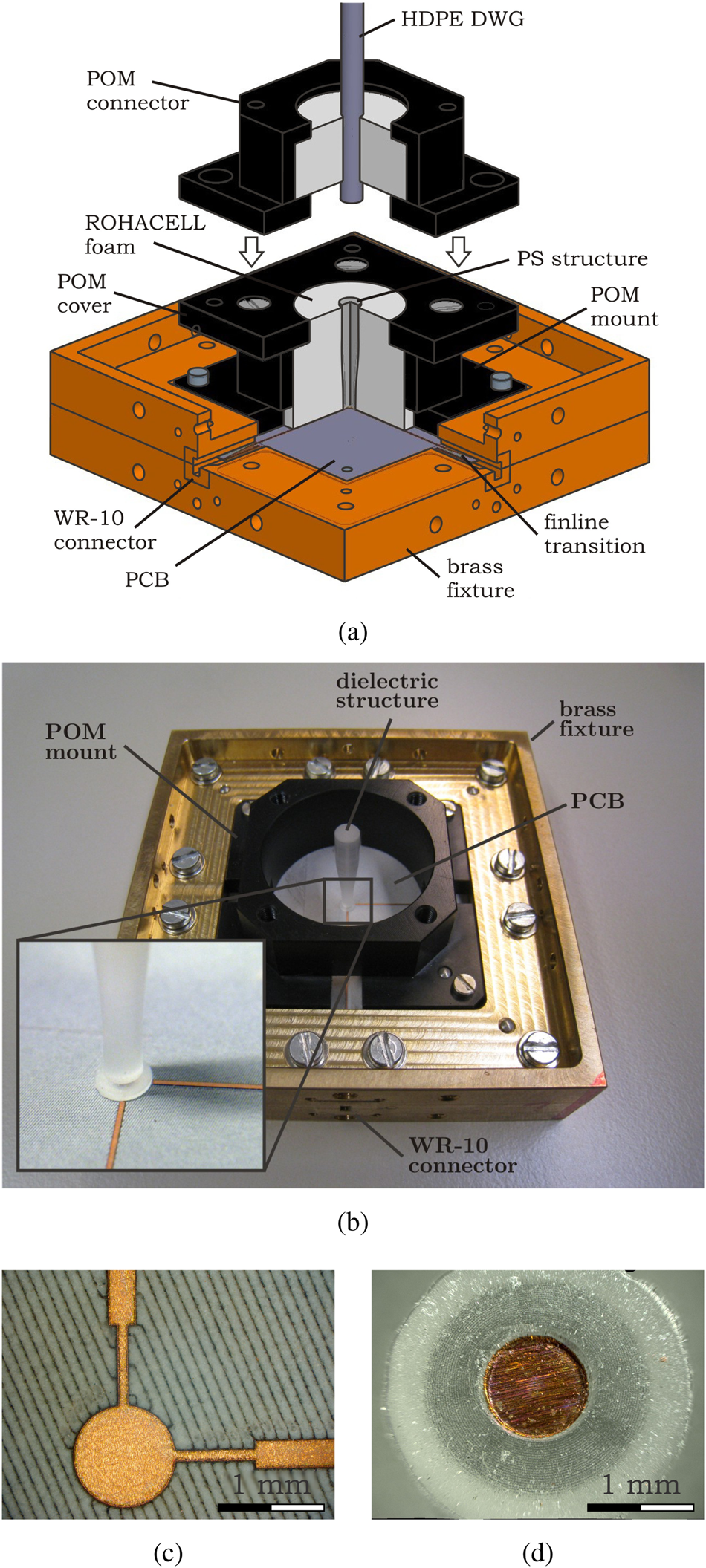
For measurements at W-band frequencies, a vector network analyzer N55250 PNA from Agilent with an N5260-6003 test set for each port is used. Both test sets provide WR-10 connectors. To connect both WR-10 test sets to the MSLs on the prototype PCBs, a fixture made of brass is applied (see Figs 5(a) and 5(b)). This brass fixture holds the PCB in place and contains two finline transitions from MSL to WR-10, one for each polarization. The dielectric structure is held by ROHACELL foam (ɛr = 1.1) (not shown in Fig. 5(b)) that is attached to the brass fixture by a housing made of polyoxymethylene (POM). Due to the low relative permittivity, ROHACELL does not affect the electrical properties of the transitions. A detachable cover (not shown in Fig. 5(b)) on top of the POM mount allows to press the solid ROHACELL foam and therefore the dielectric structure onto the PCB to maintain a reliable small z-offset.
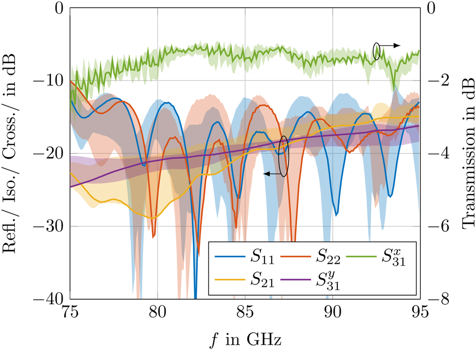
To obtain statistical significance for the measurement results, the scattering parameters of various combinations of the three PCBs and the four dielectric structures are measured. For each S-parameter, 12 combinations of PCB and dielectric structure are selected. The rotational orientation of the dielectric structure related to the PCB is chosen randomly. The scattering parameters of each transition are measured by three types of measurements. The input reflection coefficients S 11 and S 22 as well as the isolation between both MSL ports S 21 are measured by connecting both test sets to the WR-10 connectors of the brass fixture. The DWG port is matched by adding a dielectric tip of 10 mm length made of polystyrene. For this type of measurement, every dielectric structure is combined with each of the three PCBs. The transmission coefficient from MSL to the wanted polarization $S_{31}^x$ of each MSL-to-DWG transition is measured by a back-to-back setup where three DWGs (HDPE, d = 4 mm) of different lengths (l 1 = 0.236 m, l 2 = 0.506 m, l 3 = 1.010 m) are connected between both transitions. The HDPE waveguides are attached to the test structure with a POM connector as shown in Fig. 5(a). For each back-to-back PCB pair, four random pairs of dielectric structures are chosen. The crosstalk $S_{31}^y$
 is measured by a WR10-to-DWG transition presented in [Reference Meyer, Krüger, Obermeyer and Schneider20] that is flipped by 90° and connected to the DWG port of the MSL-to-DWG transitions. Exactly like in the first measurement, every dielectric structure is combined with each of the PCBs. For all measured values, the effect of the MSLs and finline transitions as well as the losses of the HDPE DWGs and WR10-to-DWG transition are removed from the measurement results. A more detailed description of the measurement setup and calculation of the S-parameter results is given in [Reference Meyer, Karau and Schneider17]. The S-parameters per transition determined by the measurements are shown in Fig. 6. The colored shadow regions indicate the variation over all measured combinations of PCB and dielectric structure for each S-parameter. The solid lines depict the measurement results for the transition with the best overall performance. Referring to the input reflection coefficients S 11 and S 22 at both MSL ports for all measured combinations, a 10 dB bandwidth of larger than 22 GHz ($26\percnt$
 ) could be achieved. The transition with the best overall performance shows a bandwidth of around 23 GHz ($27\percnt$
 ) and 24 GHz ($28\percnt$
 ) for both polarizations, respectively. The insertion loss $S_{31}^x$
 between 80 and 90 GHz varies in a range between 1.2 and 2.0 dB. On average, the insertion loss in this frequency band is better than 1.5 dB with a minimum at around 1.2 dB. In Table 2, the measured S-parameters are compared to recent publications. It can be seen that despite manufacturing tolerance, competitive values for bandwidth and insertion loss are achieved over all measured combinations. The isolation between both MSL ports as well as the crosstalk from one MSL port to the unwanted polarization in the DWG of the optimal design are lower than 15 and − 18 dB, respectively. The assumed manufacturing tolerances impair both values to 14 and − 16 dB. In comparison to the simulation results, a quite smaller variance can be observed for all S-parameters. In order to find the cause for the smaller deviations, the PCB and the dielectric structure are optically measured. It has been found that all control parameters are within their assumed tolerance range. Therefore, it is assumed that smaller tolerances for the alignment could be achieved in the prototype manufacturing process. Especially a smaller z-offset ensured by the ROHACELL foam, which presses the dielectric structure onto the PCB, is assumed to be the cause for the better performance related to the simulation results.
Measurement results of all prototype combinations (shadowed regions) and prototype with the best overall performance (solid lines) for the input reflections at both MSL ports S 11, S 22, the transmission coefficient $S_{31}^x$ as well as the isolation S 21 and crosstalk $S_{31}^y$
 .
.
Comparison of recently published vertical PCB-to-DWG transitions [Reference Yu, Liu, Ye, Ren, Liu and Gu11]
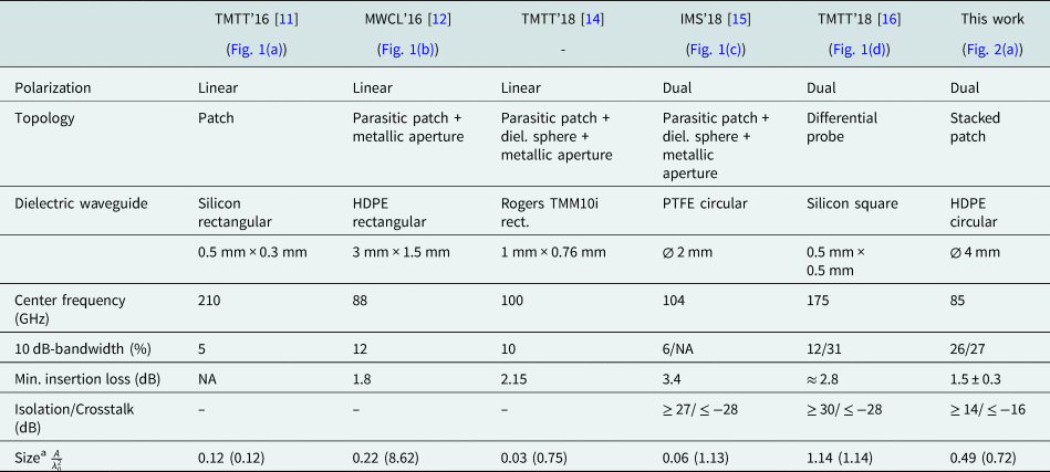
a(...) including area of dielectric and metallic structures.
Conclusion
A robust design of a broadband dual-polarized transition between an MSL and a circular DWG for mm-wave applications has been presented. A stacked-patch topology is used to reduce the space consumption on the PCB by $35\percnt$ compared to recent publications. The stacked patch is placed inside a dielectric structure which is optimized to improve the coupling between MSL and DWG. The design does not require any additional metallic apertures, which enables an easy integration into a package. An extensive sensitivity analysis has been performed by simulation and measurement to prove the transition's suitability for mass production. The sensitivity analysis identified the main influence factors of the design towards robustness of the electrical properties. Especially the size and the distance between the primary patch on the PCB and the stacked patch inside the dielectric structure are sensitive to manufacturing tolerances. It has been found that the nominal size of both patches can be optimized to either improve the insensitivity of the transmission coefficient $S_{31}^x$
 or to improve the insensitivity of isolation S 21 and crosstalk $S_{31}^y$
 . A more critical parameter is the distance between both patches. This distance is not only affected by the manufacturing tolerances of the dielectric structure but also by a possible air gap between PCB and dielectric structure. The sensitivity analysis showed a drastically increasing variance of the transmission coefficient for too large distances between both patches. For statistical significance, 12 combinations of three manufactured PCBs and four dielectric structures are measured. Comparing the measured S-parameters to recent publications, an improved 10 dB-bandwidth of greater than 22 GHz ($26\percnt$
 ) could be measured. Despite manufacturing tolerances, the insertion loss $S_{31}^x$
 in the frequency range between 80 and 90 GHz varies only between 1.2 and 2.0 dB. An isolation and crosstalk of better than 14 and − 16 dB could be obtained. The measurements showed a significantly lower variance of the S-parameters compared to the simulation results. An optical measurement of all prototype PCBs and dielectric structures suggest that the improvement was mainly caused by a better alignment of PCB and dielectric structure than assumed for the sensitivity analysis. Especially a lower z-offset due to a stable mount of the dielectric structures ensured low variance in the measurement results.
 Andre Meyer received his Diploma degree in Communication and Information Technology from the University of Bremen, Germany in 2015. He is currently a research engineer at the RF & Microwave Engineering Laboratory of the University of Bremen, working toward his Ph.D. degree in high data-rate transmission systems using dielectric waveguides.
 Martin Schneider received his Diploma and Doctorate degree in Electrical Engineering from the University Hanover, Germany, in 1992 and 1997, respectively. From 1997 to 1999, he was with Bosch Telecom GmbH, where he developed microwave components for point-to-point and point-to-multipoint radio link systems. In November 1999, he joined the Corporate Research division of Robert Bosch GmbH. As a project and section manager of the “Wireless Systems” group, he focused on research and development of smart antenna concepts for automotive radar sensors at 24 and 77 GHz. From 2005 to 2006, he was with the business unit “Automotive Electronics” of Robert Bosch GmbH where he was responsible for the “RF electronics” of automotive radar sensors. Since March 2006, he has been a full professor and head of the RF & Microwave Engineering Laboratory at the University of Bremen (Germany).


 Open access

