


I. INTRODUCTION
When the grain size of a material is refined into the nanometer range, a significant volume fraction of atoms is located in the grain boundaries, and the interfaces begin to play a dominant role in shaping both its physical and mechanical properties. The resulting ultrahigh yield and fracture strengths, as well as other beneficial properties observed in nanocrystalline metals, have continued to stimulate interest.Reference Gleiter1–Reference Lu, Shen, Chen, Qian and Lu8 Electrodeposited nanocrystalline Ni-W alloys in particular have found wide application for coatings due to their high hardness, excellent corrosion and wear resistance, and ease of processing.Reference Jones, Hamann, Lund and Schuh9–Reference Rupert and Schuh12 However, as with many coating technologies, residual stress in nanocrystalline deposits can lead to detrimental effects including a decrease in fatigue strength, cracking under service conditions, or delamination.Reference Freund and Suresh13–Reference Czerwinski and Kedzierski15 In advanced electronics and microelectromechanical systems applications, warping of the underlying fine-scale substrate features can also occur when a coating is applied or upon subsequent thermal treatment.Reference Peroulis, Pacheco, Sarabandi and Katehi16 The prospect for component failures due to such internal stress issues continues to be a technology-limiting barrier, and thus understanding their origins and controlling them is of great practical importance.
Despite the significance of residual stress in nanocrystalline coatings of every kind, quantitative measurement of these stresses is experimentally challenging due to the complexities arising from their structure and processing history. For example, whereas x-ray diffraction is a common approach to measure lattice strains, from which stresses are inferred via elasticity theory,Reference Noyan and Cohen17, Reference Cullity18 in nanocrystalline materials this method is often difficult or even impossible to apply. A small grain size in combination with microstrain leads to substantial peak broadening and even peak distortion, which can degrade the measurement accuracy of minute shifts in Bragg angles.Reference Weil19, Reference Dini20 Moreover, in the finest nanocrystalline alloys, with grain sizes below approximately 10 nm,Reference Detor and Schuh11, Reference Rupert and Schuh12 the diffraction signal is sufficiently broad as to appear more like an amorphous halo rather than the set of discrete crystallographic peaks normally required for accurate stress measurements. In such specimens, the principal reflection is distinguishable, but the higher-order reflections needed for the most accurate stress measurements are usually insufficient for quantitative analysis.
Similarly, use of the bent-strip test method common in the electrodeposition industry, which relies on measurements of residual-stress-induced substrate deflections,Reference Kouyumdjiev21–Reference Stoney23 presents additional challenges for contemporary nanocrystalline electrodeposition methods. Because these methods use long, cantilevered substrates to produce large, easily measurable deflections, the anode-cathode distance changes as a function of both time and position as plating proceeds and the substrate gradually warps.Reference Weil19 An additional issue concerns the use of very thin foil for the substrate in these measurements, which also accentuates the deflection. When combined with a thick nanocrystalline coating of substantially higher strength, there is a significant likelihood that the substrate can relieve the stress it is intended to measure by deforming plastically. Such complexities render the extraction of a stress value a qualitative exercise at best.
The family of approaches that directly measures the fine, microscale deflections associated with deposition over thick, relatively rigid substrates can in principle overcome the issues described above. Small deflections eliminate concerns about the time dependence of the current density distribution, while thick substrates mitigate the possibility of plastic deformation. For example, laser-based curvature measurements of a substrate before and after deposition are eminently viable for the study of very thin nanocrystalline films.Reference Flinn, Gardner and Nix24–Reference Zhao, Hershberger, Yalisove and Bilello29 However, the requirement of a reflective surface limits the thickness range that is accessible; thicker electrodeposited coatings (between 10 and 100 μm) of the kind used widely in industrial applications do not typically retain a mirror finish. The typical finishes (which range from matte to rough) scatter the incident laser and render curvature measurements impossible, except in the case of experimental set-upsReference Hearne and Floro30 where measurements of the reflective backside of the substrate may be possible. While the addition of so-called levelers or brighteners to induce a mirror surface finish may be possible with some specific electrodeposition baths, these additives can also generally be expected to modify the internal stress of the coating and, therefore, undermine the goal of the experiment.
In light of these issues, the residual stress state in nanocrystalline electrodeposits has rarely been studied in any systematic fashion, particularly for thicker coatings of the finest nanoscale grain sizes. Given the rapid increase in the use of electrodeposited nanocrystalline coatings in industry, there is a growing need to address this issue in a general sense as well as for specific electrodeposited materials. It is the purpose of this paper to systematically assess the residual stress in nanocrystalline Ni-W alloy electrodeposits of large thicknesses (10–100 μm) and from a bath without levelers or brighteners. We develop a straightforward procedure that involves a specific plating geometry in combination with three-dimensional profilometry, permitting reasonable quantitative stress measurements. We also explore the effects of subsequent annealing on the evolution of residual stress and offer insight into the physical origins of the intrinsic stress in Ni-W deposits.
II. ELECTRODEPOSITION OF NANOCRYSTALLINE Ni-W
Nanocrystalline Ni–W specimens were electrodeposited from an aqueous solution based on an approach developed and described in detail in Ref. Reference Detor and Schuh11. All specimens were deposited onto copper substrates of commercial purity using a platinum mesh counter electrode with a spacing of approximately 7.6 cm between the electrodes. Table I provides the composition of the plating bath, whose temperature and pH were maintained at 75 ± 2 °C and 7.4 ± 0.05, respectively. Deposition was conducted in a 4-L beaker, with continuous stirring at a rate of 200 rpm. Ammonium hydroxide additions were used to adjust the pH when necessary.
Plating bath composition used for specimen preparation.

The electrodeposition technique used here involved the application of pulsed current waveforms to tailor the composition and grain size of the deposit, after Ref. Reference Detor and Schuh11. We used a fixed forward (cathodic) baseline current density of 0.2 A/cm2 of 20-ms duration, to which we introduced a periodic 3-ms pulse ranging in amplitude (Ap) from 0 (direct current) to 0.5 A/cm2, as depicted in Fig. 1(a). Note that the amplitude of the pulse is sometimes sufficiently large that the pulse is anodic (i.e., when Ap is greater than the cathodic baseline of 0.2 A/cm2), can also describe conventional pulse plating with off-time (i.e., when Ap is equal to 0.2 A/cm2), and involves a secondary, lower cathodic current when the amplitude is small (i.e., when Ap is less than 0.2 A/cm2). Under these conditions, the resulting deposition rate varied from 23 μm/h (when Ap = 0.5) to 40 μm/h (when Ap = 0).
(a) The current waveform applied in this work consists of a fixed forward (cathodic) baseline current density of 0.2 A/cm2 of 20 -ms duration coupled with a 3-ms pulse ranging in amplitude from 0 (direct current) to 0.5 A/cm2. (b) Larger amplitude pulses lead to lower W content and because the solute atoms have a slight tendency to segregate to the grain boundary in the Ni-W system, a finer grain size is preferred for deposits with higher W content. Pulse amplitudes greater than 0.2 A/cm2 correspond to negative currents and the removal of atoms.

During the cathodic current periods, both Ni and W are deposited in a fixed ratio (with less W incorporation occurring at lower current densities), whereas W is selectively removed during periods when the current is negative as a result of its higher oxidation potential.Reference Detor and Schuh11 Each baseline period of 20 ms corresponds to the deposition of material with a volume roughly equivalent to a single monolayer. As a result, as illustrated in Fig. 1(b), pulses with larger amplitudes lead to lower W content being incorporated into the deposit. Because W exhibits a slight tendency to segregate to the grain boundaries in Ni,Reference Trelewicz and Schuh31 increasing the concentration of W promotes an increase in the total grain boundary area and, thus, drives the system toward finer grain sizes as seen in Fig. 1(b). The processing conditions described above were used to produce 10–100 μm thick films with grain sizes (compositions) ranging from 4 nm (23 at.%W) to 63 nm (2 at.%W).
Traditional metallographic techniques were used to prepare and mechanically polish cross-sections of the deposited films. Film thickness and composition (to within ±1 at.%) were measured using a Leo 438VP (Cambridge, UK) scanning electron microscope (SEM) operating at 20 kV and fitted with a calibrated energy dispersive spectroscopy (EDS) detector. A PANalytical X’Pert Pro diffractometer (Almelo, Netherlands) with a Cu Kα radiation source operating at 40 mA and 45 kV was used to obtain x-ray diffraction (XRD) peak profiles for the as-deposited films. After identifying the peak positions and calculating the full-width at half-maximum peak widths using the Jade software package (MDI, Inc., Livermore, CA), the grain sizes were quantified to within ±15% by applying the Scherrer equationReference Cullity18 to the (111) peak. Instrumental broadening effects were removed using the Cauchy-Gaussian approach.Reference Zhang, Zhou and Lavernia32 This grain size analysis technique has been shown to be accurate for Ni-W alloys,Reference Rupert and Schuh12 where the measured XRD grain sizes were verified by extensive transmission electron microscopy (TEM).
A seperate set of films was prepared for the specific purpose of assessing the elastic properties of the alloys by nanoindentation for incorporation into the residual stress calculations. A Hysitron Ubi1 indenter (Eden Prairie, MN) with a diamond Berkovich tip was used, and all tests were performed at a constant indentation strain rate under a constantly applied maximum load of 10 mN, corresponding to depths in the range of 200–250 nm. After loading, the sample was unloaded to 20% of the maximum load, and a 10 s hold was used to characterize instrumental drift. The Oliver-Pharr methodReference Oliver and Pharr33 was used to determine the reduced modulus, Er, from load-displacement curves, using a tip area function that was carefully calibrated on fused silica. The Young’s modulus of the Ni-W film was then extracted from the measured values of Er by assuming a Poisson’s ratio of νf = 0.31 for Ni-W and using the standard literature values of vi = 0.07 and Ei = 1141 GPa for the diamond tip.Reference Simmons and Wang34 A minimum of 30 indentation curves was used to calculate each of the reported modulus values.
III. RESIDUAL STRESS IN THE ELECTRODEPOSITS
Our approach to stress measurement is based upon profilometry curvature measurements. To ensure axisymmetric elastic properties, and thereby an equibiaxial stress, within the plane of the substrates, it is important to recognize that copper (our substrate material) is significantly elastically anisotropic. Through experimentation, it was determined that copper sheet metal (with a rolling textureReference Dillamore and Roberts35) could not be used effectively as a substrate due to the in-plane anisotropy of its elastic properties and anisotropic curvature development upon electroplating. To address this issue, copper disks of approximately 0.5 mm thickness were cut from an extruded 2.54-cm diameter cylindrical rod. The extrusion texture for copper is transversely (in-plane) isotropic, as are the resulting curvatures. The copper disks were mechanically polished to 800 grit, electropolished, and then electrocleaned to provide a smooth, uniform surface for plating.
Although it is common to use the linearized Stoney formula for residual stress calculations based on curvature measurements, the conditions under which it is valid (a coating to substrate thickness ratio of ∼5%Reference Freund and Suresh13) are quite restrictive and often involve deflections below the viable resolution of profilometry. Accordingly, we use the extended Stoney formula for thick filmsReference Freund and Suresh13, Reference Freund, Floro and Chason36 to determine the average residual stress, σ, from the change in curvature, ΔK, of the substrate before and after deposition:
where Mx and hx represent the biaxial modulus and thickness of the substrate (x = s) or film (x = f), respectively, while M and H refer to a ratio of the film to the substrate property. Film thickness was calculated from an average of nine thickness measurements along the middle one-third region during SEM characterization, and substrate thickness was measured at five locations using a micrometer and then averaged.
Based on the Young’s modulus data determined by nanoindentation, values for the biaxial modulus were calculated using the following formulaReference Freund and Suresh13:
The measured values of Mf were 377, 350, 358, 326, 326, and 298 GPa for compositions of 1.5, 2.6, 7.4, 15.2, 17.9, and 21.3 at.% W, respectively; a linear fit through these data was used to infer the modulus at other intermediate compositions.
As noted earlier, the extrusion texture for copper is transversely isotropic, and Schmid and Wassermann found that that the preferred orientation of extruded pure copper metal parallel to the fiber axis has a relative proportion of 40 vol% <100> and 60 vol% <111>.Reference Dillamore and Roberts35 The effective biaxial moduli for the (100) and (111) planes for copper were calculated as 114.8 GPa and 261.0 GPa, respectively, fromReference Freund and Suresh13:
where the elastic constants for copper were taken to be C11 = 168.4 GPa, C44 = 75.4 GPa, and C12 = 121.4 GPa.Reference Simmons and Wang34 A simple rule-of-mixtures using these values yielded a value of 202 GPa for the effective biaxial modulus, Ms, of the extruded copper rod substrate material.
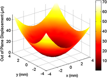
To measure the curvature change associated with deposition, three-dimensional traces of the middle one-third region of the sample surface, as represented by the image in Fig. 2, were obtained using a KLA-Tencor P-16+ profilometer (Milpitas, CA) equipped with a 2-μm stylus. Three-dimensional profilometry provides a more robust analysis method as compared with its two-dimensional counterpart, ensuring that the maximum curvature is always measured.
A representative three-dimensional profilometry trace of the middle one-third region of a copper substrate.
A nonlinear least squares approach was used to fit an ellipsoid to the sample surface, and the mean curvature of the ellipsoid, K, was calculated at its vertex (0,0, zo):
where a,b, and c are the fitted ellipsoid radii.
An important obstacle to the use of the extended Stoney formula with electrodeposits is achieving a uniform film thickness, hf, which is complicated by a non-uniform current density distribution that results in thicker deposits near the edges of the substrate, known commonly as the “edge effect”. This thickness non-uniformity is of concern because a portion of the resulting measured curvature of the substrate would result not from the true bending of the substrate but instead from the thickness gradient across the sample. We have estimated the error from such artificial curvatures to be on the order of ∼150 MPa.
To improve the current density distribution over the surface area of the substrate, an auxiliary cathode (or current thief) was constructed.Reference Mehdizadeh, Dukovic, Andricacos, Romankiw and Cheh37 Copper wire of 0.4 mm diameter was electrically connected to the substrate and positioned around its perimeter at a constant offset distance of 1 mm. Note that the full exposed area of the substrate and the thief were taken into account when calculating the applied current necessary to obtain the current density waveform illustrated previously in Fig. 1(a). In Fig. 3, we have cross-sectioned two deposits prepared using a pulse amplitude of 0 A/cm2 to compare the thickness distribution, as measured by SEM. The current thief redistributes the electric field near the edges of the substrate, leading to a significantly more uniform deposit near the substrate edges. In the middle third of the substrate, which is the region from which we take our curvature measurements, the film is effectively uniform in thickness.
Cross-sectional view of the radius of two Ni-W films prepared using a pulse amplitude of 0 A/cm2 of approximately 75 μm thickness, illustrating an increasing film thickness in moving from the center (0 mm) to the edge of the films (12.7 mm). It is clear that the addition of a current thief significantly improves the deposit uniformity.

The residual stress was characterized for 16 samples deposited using processing conditions ranging in pulse amplitude from 0–0.5 A/cm2 with resulting compositions, grain sizes, and thicknesses varying from 2–23 at.% W, 4–63 nm, and 10–98 μm, respectively. Table II summarizes the conditions used to produce each specimen.
Processing conditions and characterization of electrodeposited Ni-W films.

To determine the intrinsic residual stress state of the films, the extrinsic stress due to the difference in thermal contraction between the material being deposited (Ni-W) and the substrate (Cu) as the films cooled from the deposition temperature of 75 °C to room temperature was first calculated and subtracted out. The extrinsic stress was found to vary from 77–90 MPa (compressive) using the following relationshipReference Doerner and Nix38:
where thermal expansion coefficients, α, of 16.5·10−6, 13.4·10−6, and 4.50·10−6 K−1 (Ref. Reference Lide39) were used for Cu, Ni, and W, respectively, and a rule of mixtures was applied to estimate the thermal expansion coefficient of the Ni-W alloy films. The resulting intrinsic residual tensile stress in these as-deposited Ni-W films, σas-dep, was observed to vary from approximately 300–1300 MPa across the experimental space, as illustrated in Fig. 4(a). Propagation of the error due to the relative errors in curvature (±2%), substrate thickness (±5%), film thickness (±2%), and biaxial modulus (±15%) was used to calculate the error bars on stress (±9%) shown in this figure.
(a) The intrinsic residual stress of the as-deposited Ni-W films ranges from approximately 300–1300 MPa for pulse amplitudes ranging from 0 to 0.5 A/cm2. (b) Replotting this data as a function of grain size in a semilogarithmic fashion better represents the range of accessible grain sizes. A rapid increase in residual stress occurs with an increase in grain size below ∼15 nm while further increases in grain size result in a gradual decrease in stress.

Figure 4(a) compiles all the experimental data on a single axis related to a relevant processing variable (amplitude of the pulsed current, Ap); however, the data show a great deal of scatter and no clear trend with this single parameter. We attribute this scatter to the complex interdependency of processing conditions, grain size, and composition and note that the data in Fig. 4(a) correspond to different film thicknesses as well. As a result, presenting the data in this raw form obscures the most important physical trends. In Fig. 4(b), we replot the same data as a function of grain size (using a semilogarithmic scale to better represent the range of accessible grain sizes). We now observe a strong and reproducible trend wherein the stress level appears to first increase rapidly with grain size for the smallest grain sizes (<15 nm) and then gradually decreases beyond this point.
IV. RESIDUAL STRESS EVOLUTION DURING ANNEALING
To investigate the evolution of the stress state after annealing, the Ni-W films were annealed at 200 °C. Intermittently, after 1, 2, 4, 6, and 9 h, the films were cooled back to room temperature and their curvatures were measured to determine the residual stress using the approach outlined earlier. In all the samples, the resulting stress levels were observed to increase significantly in the first 1–2 h of annealing and then gradually reach a plateau as shown for some typical films in Fig. 5; no significant change in stress was observed for longer times. No evidence of grain coarsening has been observed in prior studies of electrodeposited Ni-W alloys after annealing for 24 h at temperatures up to 300 °C.Reference Detor and Schuh40 In the present work, the grain size of select samples was measured before and after annealing, verifying this expectation, and the results are provided in Table II.
Representative curves showing the evolution of residual stress in the Ni-W films. A significant increase in stress occurs within the first 1–2 h of annealing at 200 °C and eventually a plateau is reached. No significant increase in stress is apparent after 9 h of annealing.

The total increase in stress at the exhaustion of the annealing process (Δσ) can be extracted from Fig. 5 and is plotted in Fig. 6(a); the final residual stress of the films after annealing is presented in Fig. 6(b), in comparison with the as-deposited stress. In both cases, we observe the same concave-downward trend, with significant increases as the grain size rises to 15 nm and a gradual decrease thereafter. The similar trend in all three cases suggests that a similar mechanism for stress generation might be at play during both the deposition process and postdeposition annealing. This is a point to which we will return in the discussion.
(a) The increase in residual stress occurring during the annealing process ranges from approximately 300–1000 MPa and (b) the maximum residual stress of the annealed Ni-W films ranges from approximately 600 to 2300 MPa for grain sizes between 4 and 63 nm.

V. PHYSICAL ORIGINS OF RESIDUAL STRESS
The above results demonstrate that significant tensile residual stress can be present in nanocrystalline Ni-W in the as-deposited state and that this stress state can also evolve upon annealing. In fact, the residual stress can reach values as high as 2.3 GPa, which is close to the nominal strength of nanocrystalline Ni-W (∼2.5–3 GPa as inferred from indentation dataReference Rupert41, Reference Trelewicz and Schuh42). These data also exhibit interesting trends with respect to processing conditions and grain size, and these trends may provide some clues as to the origin of the residual stresses and their evolution and may also point the way to controlling or reducing residual stress in an application setting.
The underlying principle for existing theories of intrinsic stress generation in deposited films pertain to volume redistribution and constrained shrinkage of the film. While an unconstrained film would shrink as a result of a volume decrease ∆V/V in the film, its attachment to a substrate forces the build up of a tensile stress, σ, to oppose this strainReference Doerner and Nix38:
There are many ways in which the volume of a film might change relative to the substrate. And, presumably, whatever mechanism is responsible for film shrinkage during deposition may also be relevant for the postdeposition evolution of the residual stress state, as during annealing. With quantitative data for a variety of deposition conditions, both after deposition and after subsequent annealing, the present results allow us to explore some possible physical explanations for the residual stress in the Ni-W system. In the following section, we proceed by first analyzing the possible causes of stress evolution in these films upon annealing and later return to the as-deposited state. A more detailed discussion can also be found in the thesis upon which this paper is based.Reference Ziebell43
A. Evolution of residual stress during annealing
1. Codeposited hydrogen evolution
One prominent theory for the origin of residual stresses in electrodeposits in the literature proposes that codeposited hydrogen is incorporated during deposition; its subsequent release therefore decreases the occupied volume of the specimen, creating tensile stress in the deposit.Reference Weil19 Hydrogen that evolves from the specimen during plating can thus in principle be associated with the as-deposited residual stress, while stress evolution after deposition or during annealing can be explained by hydrogen removal well after deposition. Nickel-based deposition processes are known to generally involve hydrogen incorporation,Reference Armyanov and Sotirovachakarova44–Reference Gabe46 and the present Ni-W specimens are no exception. One set of 40-μm thick deposits prepared using three distinct pulse amplitudes (Ap = 0 A/cm2, 0.3 A/cm2, and 0.5 A/cm2) were placed in a beaker of glycerin heated to 100 °C immediately after deposition, upon which hydrogen evolution was directly observed; a prodigious number of small (∼100, 1-mm diameter) bubbles were emitted from each specimen before gas evolution slowed and ceased after approximately 10 min. An identical set of deposits were allowed to outgas under vacuum at 0.2 mbar for 22 h at room temperature, which was found to release all of the hydrogen without requiring a thermal treatment; samples subjected to the vacuum conditions released essentially no gas upon subsequent immersion in glycerin at 100 °C . No observable difference in the hydrogen content for different processing conditions was apparent.
Next, to determine whether the release of hydrogen gas could be responsible for the observed volume shrinkage and resulting increase in stress occurring during annealing, three Ni-W films of varying thickness and current waveform parameters were prepared: Ap = 0.1 A/cm2, hf = 21 μm; Ap = 0.1 A/cm2, hf = 75 μm; and Ap = 0.3 A/cm2, hf = 98 μm. The curvature of each of these samples was analyzed by profilometry immediately after plating and then again after experiencing 22 h in vacuum (a treatment that, as shown above, removes the hydrogen without requiring any thermal exposure).
As shown in Fig. 7, in all three cases, we observe only a negligible change in residual stress (∼15–45 MPa) following the removal of codeposited hydrogen; this change is well within the error of the measurement (±10%) and is smaller by an order of magnitude or more than the as-deposited residual stress. This value is also far smaller than the additional increment of residual stress Δσ that is found to develop upon annealing [see Fig. 6(a)]. Accordingly, we conclude that the postdeposition release of hydrogen plays a very minor role in the final residual stress state of annealed nanocrystalline Ni-W films. Although we cannot strictly rule out a contribution of hydrogen evolution during deposition to the as-deposited residual stress, the fact that we observe no clear differences in hydrogen evolution among the various specimens, despite very large differences in their residual stress state, suggests that hydrogen plays a very minor role at best.
Only a slight increase in residual stress (∼15–45 MPa) is observed following the removal of codeposited hydrogen by outgassing under vacuum at 0.2 mbar at room temperature for 22 h. These results suggest that the postdeposition release of hydrogen plays a very minor role in the final residual stress state of electrodeposited nanocrystalline Ni-W films and would not be responsible for the large volume shrinkage observed following annealing.

2. Structural rearrangements and defect annihilation
The densification of films as a result of the coalescence of isolated deposition clusters or islands is a widely cited theory of stress generation in the literature Reference Abermann, Koch and Kramer47–Reference Nix and Clemens53; however, while this may be the most significant stress-producing process to occur in very thin, noncontinuous films, it is not clear why this theory would apply to the relatively thick films (10–100 μm thick) deposited in our study. This mechanism leads to a maximum tensile stress occurring at the point when the film first becomes completely continuous (at <100 nm thickness) followed by a gradual reduction and eventual leveling off of the tensile stress at a film thickness of approximately 200 nmReference Janda and Stefan51; with thicknesses several orders of magnitude beyond this transition, we need to consider alternative mechanisms for the present Ni-W coatings.
Another prominent stress-generating mechanism common in very thin films but also not especially relevant to our current study is the growth of a film with an epitaxial relationship to the substrate, where a mismatch between the lattice spacings of the two materials is present. The strain energy in the film increases with the thickness of this epitaxial layer until the formation of a series of misfit dislocations at the interface becomes more energetically favorable. In the present case, new nanocrystalline grains are formed every few nanometers, and at thicknesses of 10–100 μm, many grains separate the surface from the substrate; the epitaxial relationship or lack thereof at the substrate interface is not expected to be of significant consequence for the bulk of the film.
For the case of continuous metal films, a tensile stress is created when material deposited in a nonequilibrium state experiences subsequent atomic rearrangements that serve to increase the elastic strain energy while decreasing the total energy of the system.Reference Klokholm and Berry54, Reference Buckel55 The annihilation of excess vacancies, dislocations, and grain boundaries; phase transformations; precipitation; and compositional changes can all lead to densification volume changes. We may rule out several of these possibilities for the present experimental materials.
Grain growth produces a denser material because the atomic density within grain boundaries is less than that in crystals,Reference Chaudhari56 and in nanocrystalline materials, the volume fraction of grain boundaries decreases rapidly over a narrow span of grain sizes. Similarly, volume changes associated with phase transformation and particle precipitation may be involved; for example, crystallization of an amorphous structure often results in a 1–2% increase in densityReference Davis57 and the generation of large stresses. However, as noted earlier, grain coarsening, phase separation or precipitation are simply not observed in Ni-W alloys for annealing temperatures up to 300 °C for 24 h,Reference Detor and Schuh40 and this observation was verified in our specimens as well (see Table II). As a result, we can eliminate these structural changes as possible mechanisms for the stress evolution observed during annealing (see Fig. 5).
The remaining likely structural change that may be associated with stress generation in nanocrystalline Ni-W is the escape of excess vacancies, which are expected in nonequilibrium electrodeposits and whose subsequent removal is a densifying proposition. For example, one can envision lattice vacancies within the grains, which diffuse to grain boundaries and are quickly lost; the constraint of the substrate against the volume contraction leads to the development of a biaxial tensile stress. Doerner and Nix calculated the stress development in Ni from vacancy diffusion and annihilation at grain boundaries for a grain size of 30 nm and an initial vacancy volume fraction of 1% for a range of temperatures and times.Reference Doerner and Nix38 After 9 h at 200 °C (similar to our annealing treatment), the calculated stress values were only on the order of 1 MPa. Given that >1 GPa of stress evolution is seen in our specimens, it appears unlikely that loss of a realistic content of lattice vacancies could contribute significantly to stress generation in our films.
Alternatively, we may envision excess vacancies (or more aptly, excess free volume) being predominantly located in the grain boundaries and intercrystalline regions of our deposits and its shrinkage or collapse as the kinetic process controlling residual stress development. In fact, in the specific case of deposited nanocrystalline coatings, simulation work has shown that vacancies and free volume have a tendency to populate grain boundaries.Reference Ruan and Schuh58 This situation is captured by Hoffman’s grain-boundary relaxation model,Reference Doljack and Hoffman49, Reference Hoffman50, Reference Pulker59 which proposes that deposition results in grain boundaries that are more widely spaced than equilibrium boundaries. An elastic strain and tensile stress are created in the film as the atoms relax toward their equilibrium positions.
Doerner and Nix modeled this situation by considering a fine distribution of very small voids, or vacancy clusters, the surfaces of which are brought into contact by diffusional processes, driven by capillarity because the energy of the void surface is always greater than the energy of the grain boundary.Reference Doerner and Nix38 Atoms move from the grain boundary into the void, and without the constraint of the substrate, the two crystals would move toward each other. Doerner and Nix adapted a cavitation-and-sintering model of Speight and BeereReference Speight and Beere60 to analyze the rate of stress generation and provided some representative results for Ni films at a grain size of 50 nm and a void fraction of 0.003, which is a close match to the samples in our experiments. At temperatures of 75 °C and an initial void radius of 2 nm, stress levels of 1.1 GPa would be generated in approximately 8 h; it is clear that the kinetics are much quicker than those associated with vacancy annihilation from the grain interiors, and these calculations are in line with both the kinetics and the magnitudes of the stresses we measured upon annealing of nanocrystalline Ni-W.
The thermally induced relaxation of grain boundaries in electrodeposited Ni-W is also a previously documented process, as studied by Detor and Schuh.Reference Detor and Schuh40 Those authors used calorimetry, hardness measurements, and atom-probe tomography (APT) to provide evidence of grain boundary relaxation initiating at temperatures as low as 100 °C and proceeding to temperatures greater than 300 °C. Detor and Schuh did not attempt to measure volume change in their specimens due to grain boundary relaxation, but it seems clear from the above discussion that our residual stress evolution data conform to the same process they observed through other means. From these observations and the above discussion, we conclude that excess free volume—incorporated principally in the grain boundaries during deposition—and its subsequent removal, is responsible for the increase in stress observed during annealing.
3. Effects of grain size and processing on stress evolution
Having developed some insight into the mechanism for stress evolution above, we now proceed to develop expectations for how deposition parameters and nanostructure are related to the residual stress evolution in nanocrystalline Ni-W films. We have produced films with a wide range of grain sizes (4–63 nm), and across this range, the intrinsic residual stress and its evolution vary dramatically. It seems clear that there should be an effect of grain size on the stress state, given that grain boundary relaxation is identified as the main mechanism of stress development. For example, on a geometrical basis alone, we might expect that finer-grained samples would exhibit more stress evolution, as they comprise more grain boundaries to relax. More specifically, the intergranular volume fraction, or volume fraction of atoms located at grain boundaries, can be expressed by a geometrical scaling law Reference Palumbo, Thorpe and Aust61:
where d is the grain size, t is the grain boundary thickness and is assumed to be 0.5 nm, and D is the dimensionality and has a value of 3 for conventional polycrystalline structures. Under the assumption that all of the excess free volume in the film will be located at the grain boundaries, the total volume fraction of excess free volume in the as-deposited film, Vex, would be expected to be proportional to the total grain boundary volume fraction:
where F is the free volume content of an average grain boundary.
Eqs. (8) and (9) describe a simple geometrical effect: because grain boundaries are out of equilibrium and contain excess free volume in deposits, having more grain boundaries means incorporating more free volume. This geometrical effect therefore anticipates that deposition stresses are exacerbated simply by having finer grains (more grain boundaries). However, there are additional nongeometric effects of processing that dictate just how far from equilibrium a grain boundary may be (i.e., how much free volume is stored in it). In other words, the excess free volume of the average grain boundary, F, should be expected to be a function of critical processing parameters. In particular, the pulse amplitude (Ap) represents a strong control variable that relates to the “aggressiveness” of the deposition process in the present case. As Ap is increased, more W atoms are stripped away from the deposit in an increasingly aggressive manner during the pulsing period; therefore, it is reasonable to expect an increase in the free volume incorporation with increasing Ap. Whereas the local defect production may occur anywhere on the surface during a pulse, we envision that any local free volume produced would then migrate to the grain boundary regions, where it can best be accommodated.
Thus, as a first approximation to capture the effect of processing aggressiveness, we propose that F will linearly increase with Ap:
Here, Fo represents the intrinsic free volume content produced for DC deposition (Ap = 0), and B is a proportionality constant. The form of Eq. (10) is speculative, and the two constants, B and Fo, must be treated as fitting parameters. However, we regard this form as the simplest possible model to capture the effects of pulse processing, and as we shall see, it seems to capture the most relevant physical trends.
While Eqs. (8) and (9) capture the geometrical effects of grain size (expressed in nm), Eq. (10) captures the effect of processing (expressed in A/cm2). To combine these effects into a single coherent model requires some conversion of the units. In the Ni-W system, the relationship between grain size and W content is well knownReference Detor and Schuh11 and can be described in a variety of waysReference Trelewicz and Schuh31; for our purposes here, it is simplest to use a semiempirical power-law to capture this known effect:
where G and n are 1.0 nm and −1.1, respectively. Additionally, the effect of pulsing on the incorporated W is known for this system and therefore the pulse amplitude can be converted into terms of W content, CW, as:
where the conversion constants L and C0 are −0.37 cm2A-1 and 0.23, respectively, based on the data presented in Fig. 1(b). It is important to note that Eqs. (11) and (12) are used purely for the purposes of relating composition, grain size, and pulse amplitude and do not introduce any additional physics or unknown fitting parameters; the only two physical effects specifically under consideration here are the geometrical effect of grain size [Eq. (8)] and the hypothesized effect of processing aggressiveness [Eq. (10)].
Combining Eqs. (7)–(12), we can now express the expected change in residual stress, Δσ, in a Ni-W film upon annealing out all the excess free volume in the film as:
![$$\Delta {\rm{\sigma }} =\, M_f \cdot {1 \over 3} \cdot \!\left[ {F_o + B \cdot {{\left( {{d \over G}} \right)^{{1 \mathord{\left/ {\vphantom {1 n}} \right. \kern-\nulldelimiterspace} n}} \,- \,C_o } \over L}} \right] \cdot [1 - \left( {{{d - t} \over d}} \right)^{D} ]\,\,\,\,,$$](https://static.cambridge.org/binary/version/id/urn:cambridge.org:id:binary:20151128092931294-0461:S0884291412000519_eqn13.gif?pub-status=live)
where the only adjustable parameters are B and Fo, both characteristic of processing aggressiveness. The maximum volume shrinkage, ∆V/V, occurring during annealing is synonymous with the excess free volume, Vex, stored in the as-deposited film.
The term in the first set of brackets in Eq. (13) is equal to the excess free volume content of the grain boundaries, F, and represents the processing contribution to the stress generation. The second bracketed term is the volume fraction of grain boundaries in the film, Vgb, which represents the structural or geometrical contribution. These two terms are schematically plotted in Fig. 8(a) as a function of grain size. As the pulse amplitude increases, i.e., processing becomes more aggressive, less W is incorporated in the film and the grain size rises. Thus, moving from left to right in Fig. 8(a) is associated with more aggressive processing, which leads to higher free volume storage and larger internal stress evolution. Yet, as the grain size of the sample increases, there is geometrically less grain boundary volume available to contain excess free volume, and thus, the total free volume storage is attenuated, as is the internal stress evolution. These two terms, one rising and one falling, combine to yield the concave downward trend in Fig. 8(a); this is the general form of the experimental data from Fig. 6. The biaxial modulus term also varies with composition, grain size, and possibly grain boundary state; however, modifying Mf over the full range of measured moduli values in this experimental space results in insignificant changes to ∆σ.
(a) The dashed gray curve represents the calculated excess free volume content in the grain boundaries, F(d), which is controlled by the processing parameter Ap, while the dotted black curve represents the volume fraction of grain boundary area in the film, Vgb(d), which is dependent on the structural parameter, i.e., the grain size of the film. Combining these two terms together yields the red curve, which represents the bulk excess free volume content of the film, Vex(d). Note that Vex(d) has been multiplied by a factor of 30x for ease of visibility. (b) A comparison of the experimentally determined ∆σ values as a function of grain size with those values calculated using Eq. (13).
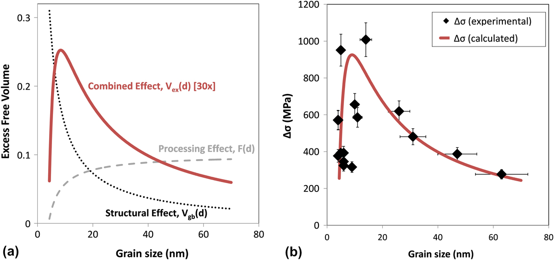
In Fig. 8(b), we explicitly fit Eq. (13) to the experimental data for the annealed films. Clearly, with only two fitting parameters (which relate only to the processing-controlled portion of the curve), we are able to reproduce the basic trend of the data. The fitted values of the adjustable parameters were found as B = 0.128 cm2A-1 and Fo = 0.019. The fitting parameter Fo seems very reasonable: it implies that in the case of DC deposition (where Ap = 0 A/cm2), the grain boundaries contain approximately 2% excess free volume. This value is comparable to the change in density in transitioning from amorphous to crystalline structures of between 1–2%Reference Chaudhari56; therefore, it is of the correct order expected for disordered grain boundaries. The parameter B essentially provides a scaling factor for how quickly additional free volume is incorporated as the pulse deposition current amplitude is increased. It is interesting to note that for our samples with the highest internal stresses [near the peak in Fig. 8(b)], the fitted value of B suggests that the grain boundary free volume content would be approximately 5%, which seems to be a reasonable magnitude for a highly disordered grain boundary structure of the kind envisioned by Hoffman.Reference Hoffman50
B. Evolution of residual stress during deposition
The above developments are most specifically related to the evolution of internal stress during annealing, although much of the logic also applies to the as-deposited condition. Returning to the as-deposited residual stress results in Fig. 4(b), we recall the striking resemblance between the shape of the σas-dep and ∆σ curves–this correlation is emphasized in Fig. 9(a), where we plot σas-dep against ∆σ. Despite some scatter, we believe that the significant degree of correlation between these parameters may speak to a common mechanism; we propose that grain boundary relaxation (i.e., the loss of grain boundary free volume) may also be a prominent factor leading to the residual stress state of the as-deposited films. Using the correlation factor of 1.4 from Fig. 9(a) along with Eq. (13), we are clearly able to reproduce the basic trend of the as-deposited residual stress data in Fig. 9(b).
(a) Correlation between the as-deposited residual stress and the maximum increase in residual stress upon annealing for the Ni-W films. This relationship points to a similar mechanism of grain boundary free volume also playing a role in the as-deposited stress state. (b) A comparison of the experimentally determined σas-dep values as a function of grain size with the calculated values based on the correlation factor of 1.4 between σas-dep and ∆σ.

A key concern for this proposal is clearly related to the issue of kinetics; a similar level of stress is generated during the deposition process (which occurs at 75 °C for between 0.25 and 4 h, depending on the film thickness and conditions used) as during the annealing treatment (which occurs at 200 °C for 9 h). Given that the kinetics of any diffusional relaxation process should be considerably slower at 75 °C than at 200 °C, it is not clear why the as-deposited residual stress levels can be so high. However, as elaborated by Doerner and Nix,Reference Doerner and Nix38 the kinetics of free volume removal is complicated by a nonlinear driving force for densification; the initial free volume fraction, scale of the free volume pockets, and characteristic diffusion distances required to annihilate free volume are all involved, and these factors can be very different during deposition vis-à-vis during annealing after deposition.
The apparent activation energy for grain boundary relaxation has been evaluated by RupertReference Rupert41 as ∼50 kJ/mol based on isothermal measurements of the strength evolution of Ni-W films; this energy scale is consistent with a process of triple junction diffusion in Ni,Reference Chen and Schuh62 which is indeed expected to be the dominant transport mechanism for our grain sizes.Reference Chen and Schuh63 Accordingly, the diffusion kinetics of annealing at 200 °C should outpace those of deposition at 75 °C by approximately a factor of 100. At the same time, however, the driving forces for densification are very different for these two stages, as the prior densification during deposition lowers the capacity for further densification upon annealing. From the calculations provided by Doerner and Nix,Reference Doerner and Nix38 it is easily possible to rationalize a factor of 100 decrease in driving force between deposition and annealing. For example, changing the initial free volume fraction in a Ni film from 1 to 0.2% slows the stress evolution by approximately a factor of 10. Furthermore, the scale of pockets into which free volume is collected (i.e., the void radius) is also important to the driving force, as the capillarity stress goes inversely with it; decreasing the free volume scale by only a factor of two leads to more than an additional order of magnitude change in the stress evolution rate.Reference Doerner and Nix38
Based on the above discussion, we envision that during deposition, free volume may be introduced with an inflated volume fraction and characteristic size scale as compared with what is retained after deposition. Although diffusion is somewhat slow at 75° C, the driving force is proportionally inflated simply due to the character of the free volume, such that the densification rate during deposition is appreciable. Accordingly, significant stress levels develop during deposition. Upon subsequent annealing, further densification can occur, and although diffusion is perhaps 100 times faster at the annealing temperature, the driving force is proportionally reduced due to prior densification during the deposition process itself. Clearly, more experimental effort aimed at in situ characterization of free volume content during deposition would be desirable to test this hypothesis. Nonetheless, it is encouraging that the above calculations based on the known activation energy for grain boundary relaxation and the Doerner-Nix model for free volume loss support its physical plausibility.
VI. CONCLUSIONS
We have illustrated a three-dimensional profilometry-based approach that permits a straight forward quantitative analysis of residual stress in thick nanocrystalline Ni-W electrodeposits. Residual stress is produced during both the deposition process and postdeposition annealing. The magnitude of the as-deposited intrinsic residual stress for Ni-W films with grain sizes of 4–63 nm ranges from approximately 300–1300 MPa (tensile) with a maximum occurring at a grain size of approximately 15 nm. The final residual stress values obtained after annealing for 9h at 200 °C range from 600–2300 MPa (tensile) with a maximum again occurring at a grain size of approximately 15 nm.
The residual stress of the as-deposited films is determined primarily by the fraction of excess free volume (or voids) in the grain boundaries of the film. The amount of free volume created and stored in the grain boundaries during the deposition process can be predicted by both the pulse amplitude, which determines the amount of free volume (or voids) created and thereby the percentage of grain boundary volume that will be composed of free volume, and the grain size, which sets the volume fraction of grain boundary area. As a result of subsequent grain boundary void shrinkage, a tensile stress develops in the film to compensate for the desired volume decrease while still maintaining the substrate dimensions. The same mechanism of grain boundary void shrinkage (or an increase in the density of the grain boundaries) is thought to be responsible for the increase in residual stress occurring during subsequent annealing.
ACKNOWLEDGMENTS
This research was supported by the US National Science Foundation, under grant DMI-0620304, the Air Force Office of Scientific Research of the Department of Defense (DoD), under the National Defense Science and Engineering Graduate (NDSEG) Fellowship, and a US National Science Foundation Graduate Fellowship. The authors would also like to thank Dr. Jason Trelewicz of MIT for providing the nanoindentation modulus data and Mr. Daniel Sauza of MIT for his assistance in the hydrogen evolution experiments.


