


I. INTRODUCTION
Over the last decade, tremendous progress has been made on the development of aberration-corrected scanning/transmission electron microscopy (S/TEM).Reference Haider, Uhlemann, Schwan, Rose, Kabius and Urban1–Reference Urban8 As a result, atomic-scale imaging and spectroscopic probing of materials appear to be routine practice.Reference Krivanek, Corbin, Dellby, Elston, Keyse, Murfitt, Own, Szilagyi and Woodruff9–Reference Jia, Mi, Urban, Vrejoiu, Alexe and Hesse14 Imaging materials at or near-realistic working conditions, or in situ S/TEM, is keeping pace with the progress of high-spatial, fast-temporal, and high-energy resolution, as exemplified by the in situ TEM observation of nanostructured materials growth,Reference Harutyunyan, Chen, Paronyan, Pigos, Kuznetsov, Hewaparakrama, Kim, Zakharov, Stach and Sumanasekera15,Reference Kim, Tersoff, Kodambaka, Reuter, Stach and Ross16 the solid–gas reaction in a catalytic system,Reference Hansen, Wagner, Helveg, Rostrup-Nielsen, Clausen and Topsoe17–Reference Yoshida, Kuwauchi, Jinschek, Sun, Tanaka, Kohyama, Shimada, Haruta and Takeda19 materials deformation behavior,Reference Shan, Mishra, Asif, Warren and Minor20,Reference Minor, Asif, Shan, Stach, Cyrankowski, Wyrobek and Warren21 particle nucleation and growth from a solution,Reference Zheng, Smith, Jun, Kisielowski, Dahmen and Alivisatos22–Reference Li, Nielsen, Lee, Frandsen, Banfield and De Yoreo24 the electrochemical deposition process,Reference Williamson, Tromp, Vereecken, Hull and Ross25 and cells in a liquid environment.Reference de Jonge, Peckys, Kremers and Piston26 This progress has benefited from both the development of a dedicated microscope that can handle certain gas pressure around the sample region, such as the environmental TEM, and the ability to manipulate and microfabricate materials at the nanoscale.
Energy storage technologies, such as lithium-ion (Li-ion) batteries, now are indispensably used for portable electronics, electric vehicles, and renewable energies.Reference Kang and Ceder27–Reference Gu, Belharouak, Genc, Wang, Wang, Amine, Gao, Zhou, Thevuthasan, Baer, Zhang, Browning, Liu and Wang31 One of the fundamental challenges for battery research is direct observation of the structural and chemical evolution of the battery components and how this directly correlates with battery properties. The ex situ method, based on electron beam imaging and spectroscopy, has been widely used for probing the structural features of a lithium battery system.Reference Retoux, Brousse and Schleich32–Reference Meng, Ceder, Grey, Yoon, Jiang, Greger and Shao-Horn39 However, due to the dynamic nature of the process, the ex situ method cannot answer some of the questions related to the dynamic process during battery operation.Reference Chen, Song and Richardson35,Reference McDowell and Cui40–Reference Kong, Kostecki, Nadeau, Song, Zaghib, Kinoshita and McLarnon43 For example, LiCoO2 has been used successfully as a cathode material for Li-ion batteries, and ex situ TEM studies indicate that there are high-density dislocations in the LiCoO2 electrode.Reference Gabrisch, Yazami and Fultz44 This observation subsequently raises several fundamental questions, such as when and how are these dislocations generated? What role do dislocations play during battery operation? And, what is the role of these dislocations on the growth of the solid electrolyte interface (SEI) layer? Answers to these questions only can be obtained by making measurements under operating conditions, such as in situ observation in a TEM. In particular, experiments must be designed to “observe” the dynamic evolution of the interface and internal structure of electrode during operation of the battery in a TEM and, ultimately,Reference Chen, Song and Richardson35,Reference Eswaramoorthy, Howe and Muralidharan45 to seek atomic and nanoscale understanding of the mechanisms associated with the following: (1) nature of the SEI layer between the electrode and the electrolyte, along with the movement of the SEI layer inside the electrode during charging/dischargingReference Bryngelsson, Stjerndahl, Gustafsson and Edstrom42,Reference Kong, Kostecki, Nadeau, Song, Zaghib, Kinoshita and McLarnon43,Reference Dedryvere, Martinez, Leroy, Lemordant, Bonhomme, Biensan and Gonbeau46 ; (2) change in the composition/structure of the SEI layer, along with the orientation/morphology of the nanostructured electrodesReference Chen, Song and Richardson35,Reference Laffont, Delacourt, Gibot, Wu, Kooyman, Masquelier and Marie Tarascon36 ; and (3) Li-ion insertion and extraction mechanisms during the electrochemical cell's operation.Reference Delmas, Maccario, Croguennec, Cras and Weill33,Reference Gibot, Casas-Cabanas, Laffont, Levasseur, Carlach, Hamelet, Tarascon and Masquelier34,Reference Nishimura, Kobayashi, Ohoyama, Kanno, Yashima and Yamada47,Reference Mauchamp, Moreau, Moncondut, Doublet, Boucher and Ouvrard48
II. CHALLENGES FOR IN SITU TEM IMAGING OF A RECHARGEABLE BATTERY
Electrochemical energy storage devices are complex, multicomponent systems that incorporate widely dissimilar phases in physical and electrical contact.Reference Tarascon and Armand30,Reference Kong, Kostecki, Nadeau, Song, Zaghib, Kinoshita and McLarnon43,Reference Dedryvere, Martinez, Leroy, Lemordant, Bonhomme, Biensan and Gonbeau46 Operation of a rechargeable battery relies critically on electron and ionic transfer across the solid–solid and solid–liquid interfaces and within each of the constituent phases. Repeated charging and discharging of the battery induces microstructural evolutions both at the interface between the electrolyte and electrode and within the electrode (active materials) due to ionic migration. Although it has been established that this structural evolution of active materials is responsible for battery failure, the mechanisms of the microstructural evolutions as a function of charging/discharging are not well understood.Reference Tarascon and Armand30,Reference Dedryvere, Martinez, Leroy, Lemordant, Bonhomme, Biensan and Gonbeau46 Overall, this imposes a fundamental scientific question regarding how the microstructures within the constituent materials and across the interface/interphase confined by the constituents evolve and affect the consequence of this structural evolution on cell properties. Due to the possibility of directly monitoring dynamic processes, in situ methods based on spectroscopies,Reference Chen, Song and Richardson35,Reference Bryngelsson, Stjerndahl, Gustafsson and Edstrom42,Reference Kong, Kostecki, Nadeau, Song, Zaghib, Kinoshita and McLarnon43,Reference Eswaramoorthy, Howe and Muralidharan45,Reference Dedryvere, Martinez, Leroy, Lemordant, Bonhomme, Biensan and Gonbeau46 atomic force microscopy (AFM),Reference Kong, Kostecki, Nadeau, Song, Zaghib, Kinoshita and McLarnon43,Reference Brazier, Dupont, Dantras-Laffront, Kuwata, Kawamura and Tarascon49 and SEM imagingReference Lux, Schmuck, Rupp, Kern, Appetecchi, Passerini, Winter and Balducci50,Reference Lewandowski and Świderska-Mocek51 have provided useful information regarding the structural evolution of the electrode materials during a battery's operation.Reference Brazier, Dupont, Dantras-Laffront, Kuwata, Kawamura and Tarascon49,Reference Yamamoto, Iriyama, Asaka, Hirayama, Fujita, Fisher, Nonaka, Sugita and Ogumi52–Reference Huang, Zhong, Wang, Sullivan, Xu, Zhang, Mao, Hudak, Liu, Subramanian, Fan, Qi, Kushima and Li60 Because of the TEM's high-vacuum operation and the vacuum incompatibility of liquid electrolyte used for most rechargeable batteries, including the Li-ion battery, the fundamental challenge is the integration of the liquid electrolyte and electrode system in the TEM's high-vacuum column.
III. IN SITU TEM STUDY OF RECHARGEABLE BATTERIES
Three strategies have been explored for this in situ TEM study of batteries, including open-cell configuration, closed liquid-cell configuration, and a whole solid-state battery.
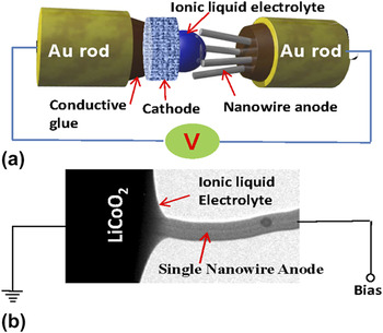
A. Open-cell configuration using ionic liquid-based electrolyte
Over the last few years, substantial progress has been made toward developing methodologies for in situ direct observation of structural and chemical evolution of electrodes used for Li-ion batteriesReference Brazier, Dupont, Dantras-Laffront, Kuwata, Kawamura and Tarascon49,Reference Wang, Xu, Liu, Choi, Arey, Saraf, Zhang, Yang, Thevuthasan, Baer and Salmon53,Reference Wang, Xu, Liu, Zhang, Saraf, Arey, Choi, Yang, Xiao, Thevuthasan and Baer54,Reference Huang, Zhong, Wang, Sullivan, Xu, Zhang, Mao, Hudak, Liu, Subramanian, Fan, Qi, Kushima and Li60–Reference Mai, Dong, Xu and Han69 —most notably, the development of an in situ TEM cell based on an open-cell configuration. The fundamental concept of the open-cell configuration for in situ TEM studies of the Li-ion battery was pioneered by Wang et al.Reference Wang, Xu, Liu, Choi, Arey, Saraf, Zhang, Yang, Thevuthasan, Baer and Salmon53 and Huang et al.Reference Huang, Zhong, Wang, Sullivan, Xu, Zhang, Mao, Hudak, Liu, Subramanian, Fan, Qi, Kushima and Li60 The basic operating principle of the cell is schematically illustrated in Fig. 1, where the ionic liquid was used as an electrolyte.Reference McDowell and Cui40,Reference Wang, Xu, Liu, Choi, Arey, Saraf, Zhang, Yang, Thevuthasan, Baer and Salmon53,Reference Huang, Zhong, Wang, Sullivan, Xu, Zhang, Mao, Hudak, Liu, Subramanian, Fan, Qi, Kushima and Li60,Reference Liu, Zhang, Zhong, Liu, Zheng, Wang, Cho, Dayeh, Picraux, Sullivan, Mao, Ye and Huang63 The essential components of the cell are a single nanowire as the observable electrode, vacuum-compatible ionic liquid as the electrolyte, and LiCoO2 as the counter electrode. A typical ionic liquid electrolyte is lithium bis(trifluoromethanesulfonyl)imide (LiTFSI) dissolved in a hydrophobic ionic liquid 1-butyl-1-methylpyrrolidium (P14) TFSI (P14TFSI). The overall composition of the electrolyte is 10% LiTFSI in P14TFSI. The open-cell configuration offers the possibility of atomic-level spatial resolution and analytical capability to study Li-ion insertion mechanisms into electrode materials during the charge/discharge cycles.Reference Ghassemi, Au, Chen, Heiden and Yassar65,Reference Ghassemi, Au, Chen, Heiden and Yassar70–Reference Yang, Huang, Huang, Fan, Liang, Liu, Chen, Huang, Li, Zhu and Zhang73 Since its invention, this technique has helped to reveal many details with respect to the lithiation mechanisms and structural evolution behavior of a range of materials, especially anode materials including Si,Reference McDowell, Ryu, Lee, Wang, Nix and Cui61–Reference Ghassemi, Au, Chen, Heiden and Yassar65,Reference Ghassemi, Au, Chen, Heiden and Yassar70,Reference Yang, Huang, Huang, Fan, Liang, Liu, Chen, Huang, Li, Zhu and Zhang73,Reference Liu, Zhong, Huang, Mao, Zhu and Huang74 Ge,Reference Liu, Huang, Picraux, Li, Zhu and Huang75 Al2O3,Reference Liu, Hudak, Huber, Limmer, Sullivan and Huang76 SnO2,Reference Wang, Xu, Liu, Zhang, Saraf, Arey, Choi, Yang, Xiao, Thevuthasan and Baer54,Reference Huang, Zhong, Wang, Sullivan, Xu, Zhang, Mao, Hudak, Liu, Subramanian, Fan, Qi, Kushima and Li60,Reference Nie, Gan, Cheng, Asayesh-Ardakani, Li, Dong, Tao, Mashayek, Wang, Schwingenschlögl, Klie and Yassar72,Reference Zhang, Liu, Perng, Cho, Chang, Mao, Ye and Huang77,Reference Zhong, Liu, Wang, Mao and Huang78 ZnO,Reference Kushima, Liu, Zhu, Wang, Huang and Li79 graphene,Reference Liu, Wang, Liu, Zheng, Kushima, Huang, Zhu, Mao, Li, Zhang, Lu, Tour and Huang80 Sn,Reference Li, Wang, Feng, Mao, Liu, Mao and Wang81 and carbon nanotubes.Reference Liu, Zheng, Liu, Huang, Zhu, Wang, Kushima, Hudak, Huang, Zhang, Mao, Qian, Li and Huang82 It has been noticed that the ionic liquid will spread along the nanowire surface to form a thin layer of coating. Therefore, this configuration can, in some degree, mimic the real battery configuration such that the liquid electrolyte forms a conformal coating around the active component in the electrode. The drawback of this method is the polymerization of the ionic liquid electrolyte under the imaging electron beam. As such, the cell only can be cycled several times, which is far short for revealing the structural evolution of the electrode materials relevant to a real battery.
(a) Schematic drawing showing the experimental setup of the open-cell approach using ionic liquid as the electrolyte, (b) TEM image showing a working nanobattery in TEM column, where the single nanowire anode can be imaged during charge and discharge of this nanobattery.
B. Open-cell configuration based on Li metal and metal oxide as the electrolyte
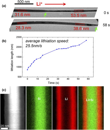
A variation of the open-cell configuration based on an ionic electrolyte (previously described) is the open-cell configuration using lithium oxide as the electrolyte. In this configuration, a Li metal is used as the anode, and a single nanowire is used as the cathode (shown schematically in Fig. 2). During insertion of the TEM holder into the TEM column, the Li metal surface is instantaneously oxidized to form a thin layer of Li2O, covering the surface of the Li metal. It is this layer of Li2O that serves as a solid electrolyte.Reference Wang, Yu, Chen, Wu, Pereira, Thornton, Van der Ven, Zhu, Amatucci and Graetz67,Reference Islam and Bredow83,Reference Liu, Zheng, Zhong, Huang, Karki, Zhang, Liu, Kushima, Liang, Wang, Cho, Epstein, Dayeh, Picraux, Zhu, Li, Sullivan, Cumings, Wang, Mao, Ye, Zhang and Huang84 In a typical example, a Si nanowire is used as one electrode, Li2O on Li metal is the solid electrolyte, and a bulk Li metal is the counter electrode. In principle, the battery assembled in this way is a charged battery, and connecting the circuit will lead to the discharging process. However, this will not be the case due to the low conductivity of the Li ion in Li2O at room temperature.Reference Islam and Bredow83 A negative potential of typically 2–4 V normally is applied between Si and Li to drive Li ions into Si. The propagation of the lithiation front can be clearly visualized by TEM imaging. The open-cell configuration offers the advantage of high spatial resolution imaging and chemical composition analysis by spectroscopic method. In a typical example, Fig. 3 shows the measured lithiation length of Si as a function of lithiation time, illustrating near-parabolic lithiation behavior. Simultaneously, the chemical composition evolution can be mapped using electron energy loss spectroscopy, or EELS.Reference Liu, Zhang, Zhong, Liu, Zheng, Wang, Cho, Dayeh, Picraux, Sullivan, Mao, Ye and Huang63,Reference Wang, Li, Wang, Xu, Liu, Gao, Kovarik, Zhang, Howe, Burton, Liu, Xiao, Thevuthasan and Baer64 The silicon map is obtained by an integration of Si L edges (99–170 eV), and the Li map is acquired by an integration of Li K edges (55–85 eV) after background subtractions. Notably, this type of experiment is not a real rechargeable battery. However, the structural response of Si with the Li-ion insertion adequately simulates what happens in a real battery. Therefore, this open-cell configuration provides a quick and convenient way for probing the intrinsic response of material to Li-ion insertion or extraction. A similar principle can be used with other metallic ion systems for studying ionic insertion and extraction behavior, such as in Na-, Mg-, and Ca-ion batteries.Reference Liu, Zheng, Zhong, Huang, Karki, Zhang, Liu, Kushima, Liang, Wang, Cho, Epstein, Dayeh, Picraux, Zhu, Li, Sullivan, Cumings, Wang, Mao, Ye, Zhang and Huang84 Another variation of the open-cell configuration has been developed by others using a standard TEM grid as described by Wang et al.Reference Miller, Proff, Wen, Abraham and Bareño66 The advantage of using a TEM grid is that it can increase the system's stability, affording high spatial resolution imaging.
(a) Schematic drawing showing the experimental setup of the open-cell approach using Li metal as the lithium source and Li2O as the solid electrolyte, (b) TEM image of a nanobattery with a single nanowire as cathode, which allows the direct observation of the structural and chemical evolution during charge and discharge.

The lithiation process observed using an open-cell configuration for Si. (a) Progression of lithiation of Si in a core–shell fashion. (b) Measured lithiation length as a function of time. The average lithiation speed is ∼25.5 nm/s. In (a), the Li+ diffusion direction is labeled by the red arrows, and the lithiation reaction fronts are marked by green arrows. The electron dose is 1.55 A/m2. (c) STEM-high-angle annular dark-field (HAADF) image and EELS mapping of Si, Li, and overlaid Si and Li composite, revealing a core–shell lithiation.
C. The closed electrochemical liquid-cell for direct correlation of structure and electrochemical properties
In situ TEM work conducted on open-cell configurations has provided insightful information on the structural and chemical evolution of electrodes upon lithiation/delithiation. However, three typical deficiencies are associated with the open-cell configuration. First, for the open-cell, the electrolyte is only in point contact with the electrode, which may inadvertently modify the diffusion pattern of the Li ion in the electrode. Therefore, what has been observed is not necessarily a representative case for the electrode being fully immersed in the liquid electrolyte in a real battery. Second, in using Li2O as the electrolyte, a large overpotential is normally applied to drive the Li ions into the electrode, which may change the kinetics and phase behaviors of solid-state electrode lithiation. Third, using the ionic liquid or Li2O electrolyte excludes some of the fundamental processes that occur only in real electrolytes and battery-operating conditions, such as the interaction between the electrolyte and electrode and the SEI layer formation.
To address the shortcomings of the open-cell (already described), recent work has focused heavily on developing a liquid-cell for in situ or more precisely operando TEM studies of Li-ion batteries using a battery-relevant liquid electrolyte and a lithium metal counter electrode. The in situ TEM study of electrochemical processes was initiated following the work depositing copper nanoparticles from a CuSO4 electrolyte under galvanostatic conditions using a liquid-cell into the TEM column.Reference Williamson, Tromp, Vereecken, Hull and Ross25 Since then, the microfabricated liquid-cell concept has inspired rapid development of in situ TEM imaging under liquid or gas environments for which most of the studies have focused on nucleation and growth of nanoparticles, a process that is essentially stimulated by the imaging electron beam.Reference Zheng, Smith, Jun, Kisielowski, Dahmen and Alivisatos22,Reference Liao, Cui, Whitelam and Zheng23,Reference Meng Gu, Kushima, Shao, Zhang, Liu, Browning, Li and Wang85–Reference de Jonge and Ross90 The progression of liquid-cell microscopy, in turn, has helped push the development of an electrochemical cell process.Reference Woehl, Park, Evans, Arslan, Ristenpart and Browning91,Reference Chen, Noh, Wen and Dillon92,Reference Evans, Jungjohann, Wong, Chiu, Dutrow, Arslan and Browning93 This approach already has allowed direct observation of beam-sensitive systems, such as macromolecular complexesReference Evans, Jungjohann, Wong, Chiu, Dutrow, Arslan and Browning93,Reference Mirsaidov, Zheng, Casana and Matsudaira94 and soft materials,Reference Huang, Liu, Chuang, Hsieh, Tsai, Wu, Tsai, Mirsaidov, Matsudaira, Chang, Tseng and Chen95,Reference Proetto, Rush, Chien, Abellan Baeza, Patterson, Thompson, Olson, Moore, Rheingold, Andolina, Millstone, Howell, Browning, Evans and Gianneschi96 and of processes that span from electrochemical deposition of metalsReference Williamson, Tromp, Vereecken, Hull and Ross25,Reference White, Singer, Augustyn, Hubbard, Mecklenburg, Dunn and Regan97 to growth of different nanostructures.Reference Liao, Cui, Whitelam and Zheng23,Reference Evans, Jungjohann, Browning and Arslan86,Reference Jungjohann, Bliznakov, Sutter, Stach and Sutter88,Reference Woehl, Evans, Arslan, Ristenpart and Browning89,Reference Zheng, Claridge, Minor, Alivisatos and Dahmen98,Reference Parent, Robinson, Cappillino, Hartnett, Abellán, Evans, Browning and Arslan99
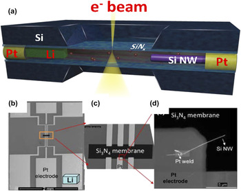
Gu et al.Reference Gu, Parent, Mehdi, Unocic, McDowell, Sacci, Xu, Connell, Xu, Abellan, Chen, Zhang, Perea, Evans, Lauhon, Zhang, Liu, Browning, Cui, Arslan and Wang100 successfully demonstrated the first working closed liquid-cell for a rechargeable battery (schematically illustrated in Fig. 4). Subsequently, similar devices have been demonstrated by other groups as well.Reference Gu, Parent, Mehdi, Unocic, McDowell, Sacci, Xu, Connell, Xu, Abellan, Chen, Zhang, Perea, Evans, Lauhon, Zhang, Liu, Browning, Cui, Arslan and Wang100–Reference Unocic, Sacci, Brown, Veith, Dudney, More, Walden, Gardiner, Damiano and Nackashi104 In a typical example, the working electrode is a single Si nanowire, while the counter electrode is a Li metal. This electrode geometry was implemented using a SiNx membrane deposited on Si chips (illustrated in Fig. 4). An ∼50 nm-thick SiNx membrane is used to seal the liquid while still allowing transmission of the high-energy electrons for imaging. The biasing chip has six Pt electrodes. The Pt electrodes extend from the SiNx window to the edge of the chip, connecting the electrode to the outside circuit. A single or multiple Si nanowires can be mounted on one of the Pt electrodes using focused ion beam (FIB) manipulation and Pt deposition welding. The welded Si NWs extend to the electron-transparent SiNx membrane region to enable imaging of the nanowire in electron transmission mode. A droplet of 1.0 M of lithium perchlorate, LiClO4—containing mixed ethylene carbonate (EC) and dimethyl carbonate (DMC) electrolytes (3:7, v/v)—was applied to the top surface of the SiNx membrane (fully immersing all Pt electrodes, Li metal, and Si NWs), and a blank chip with a SiNx membrane facing down was placed over the biasing chip to seal the liquid electrolyte. The sealing is completed based on a three-O-ring technique, and the whole device is implanted on a biasing in situ TEM liquid holder (Hummingbird Scientific, Lacey, WA). The assembly process was completed in an argon-filled glove box to avoid atmospheric degradation of the electrolyte/electrodes. The viewing window dimensions are 50 μm × 50 μm. The normal thickness of liquid layer is 500–1000 nm. However, after loading the cell into the TEM column, the membrane will bulge outward due to the pressure differences.
(a) Schematic drawing showing the setup of the liquid-cell battery. (b) SEM image of the inner side of the biasing chip, (c) magnified view of the region labeled by the orange rectangle, and (d) SEM image showing the welded Si NW electrode onto the Pt contact. Note that the Li location is labeled by the light blue color object in panel (based on the TEM holder system developed by Hummingbird Scientific).
In situ liquid-cell TEM observation of the lithiation of Cu-coated Si (Cu–Si) NW. (a) TEM image showing the pristine state of the Cu–Si NW at 0 s, and (b) core–shell formation of the Cu–Si NW during lithiation at 2462 s. (c) Current versus voltage plot during the delithiation process. (d–f) STEM Z-contrast image and bright-field images of the nanowire at different states of delithiation (the left side of each panel in (d–f) shows the HAADF Z-contrast image, and the right side shows the corresponding bright-field STEM image acquired simultaneously). Note that the white arrows in (d) indicate the deposited Pt markers for Ref. Reference Gu, Parent, Mehdi, Unocic, McDowell, Sacci, Xu, Connell, Xu, Abellan, Chen, Zhang, Perea, Evans, Lauhon, Zhang, Liu, Browning, Cui, Arslan and Wang100.

D. Direct in situ TEM observation of lithiation/delithiation of Si, Li ion transport in LiFePO4, and SEI layer formation on an Au electrode
The lithiation of Cu-coated crystalline Si NW in the liquid-cell is performed by holding the voltage of the Cu–Si anode to ∼0.03 V range. The structural evolution of the nanowire upon lithiation is illustrated by the captured video frames shown in Figs. 5(a) and 5(b). The lithiation of the Si nanowire immersed in the liquid electrolyte progresses in the core–shell fashion. The total diameter of the wire changes from 100 nm to 391 nm at 2462 s. Based on the projected radial dimension increase, this indicates that the radial direction of this wire is along the <110> direction (maximum volume expansion direction of Si upon lithiation).Reference Lee, McDowell, Choi and Cui41,Reference Yang, Huang, Huang, Fan, Liang, Liu, Chen, Huang, Li, Zhu and Zhang73 The increase in the diameter is quicker at the beginning of lithiation and slows down with progression of the lithiation process. This phenomenon is related to the interface stress generated by the volume expansion, which limits the diffusion of Li ions further into the core. The slowdown of lithiation after partial lithiation also has been consistently reported by earlier researchers.Reference McDowell, Ryu, Lee, Wang, Nix and Cui61,Reference Gu, Li, Li, Hu, Zhang, Xu, Thevuthasan, Baer, Zhang, Liu and Wang71,Reference Liu, Fan, Yang, Zhang, Huang and Zhu105
The delithiation process of a pure Si nanowire is shown in Figs. 5(d)–5(f). The delithiation process is performed by scanning the voltage from 0 to 0.65 V at an increment of 0.3 mV/s, and the current versus voltage curve is plotted in Fig. 5(c). The image shown in Figs. 5(d)–5(f) represents a pair of dark-field (left) and bright-field (right) STEM images. In Fig. 5(d), the white arrows in the dark-field image indicate the Pt markers, which were intentionally deposited on the nanowire using electron beam deposition in the FIB SEM. The Pt markers show a higher Z-contrast in the dark-field images, highlighting the wire's positions in the liquid-cell. The diameter of the lithiated Si nanowire is 195 nm [shown in Fig. 5(d)]. The diameter of the nanowire shrank when the voltage scanned to 0.45 V, as shown in Fig. 5(e). The diameter kept decreasing as lithium ions were extracted. In the end, the diameter shrank to ∼92 nm in the final delithiated state, as shown in Fig. 5(f) at 0.65 V. The large volume change, as measured based on the reduction in diameter from 195 to 92 nm, indicates that most of the Li ions were extracted during this process.
Using a closed liquid-cell configuration, Holtz et al.Reference Holtz, Yu, Gunceler, Gao, Sundararaman, Schwarz, Arias, Abruña and Muller101 studied the Li-ion transport kinetics and degradation mechanisms in LiFePO4 particles during the charge/discharge cycles. Observations of Li transport are very challenging. However, in their experiment, they used energy-filtered TEM imaging by selecting a valence energy loss peak at 5 eV, which is unique for FePO4 but not for LiFePO4. Therefore, environmental transmission electron microscopy (ETEM) images captured with the energy window selected at this region can be used to probe the phase transition and Li transport characteristics between LiFePO4 and FePO4. This method allowed Holtz et al.Reference Holtz, Yu, Gunceler, Gao, Sundararaman, Schwarz, Arias, Abruña and Muller101 to determine the lithiation state of a LiFePO4 electrode and surrounding aqueous electrolyte in real time with nanoscale resolution during electrochemical charge and discharge, enabling them to track lithium transfer between the electrode and electrolyte and image charging dynamics in the cathode.
Zeng et al.Reference Zeng, Liang, Liao, Xin, Chu and Zheng103 reported the formation of the SEI layer on an Au electrode during electrochemical lithiation and delithiation of Au anodes in lithium hexafluorophosphate (LiPF6)/EC/diethyl carbonate (DEC) electrolyte. Upon the cyclic voltammetry (CV) scan, they noticed the inhomogeneous lithiation of the Au electrode, lithium metal dendritic growth, electrolyte decomposition, and SEI formation. The SEI layer growth appears to be concurrently accompanied by the Li dendrite growth. The SEI layer is observed to uniformly develop on the Au electrode surface. In a similar effort, Sacci et al.Reference Sacci, Dudney, More, Parent, Arslan, Browning and Unocic102 observed the SEI layer on an Au electrode in 1.2 M LiPF6 EC/DMC battery-grade electrolyte. They noticed that SEI formed prior to the deposition of Li. Most dramatically, they found that the SEI layer shows a feature of dendritic morphology rather than a uniform layer: the dendritic SEI forms prior to Li deposition, and the SEI layer remains on the surface after Li electrodissolution. Therefore, the formation of SEI dendrites begins prior to Li deposition, suggesting that the electrolyte composition (and its electrodecomposition) affects Li deposition. It should be noted that for the case of the SEI layer growth work, no Li source is supplied in the liquid-cell. All observed phenomena result from the decomposition and deposition of the ions from the electrolyte. Even if a CV scan is done to offer a general view of the system's electrochemical behavior, more systematic work must be carried out with a proper Li source and a reference electrode.
E. Solid-state battery configuration
The solid-state battery configuration using a solid electrolyte provides another option to probe the structural and chemical evolution of electrode materials. For the solid-state configuration, it may be related to the solid-state system as a battery itself or as a platform for in situ TEM studies of a battery system.Reference Wang, Xu, Liu, Choi, Arey, Saraf, Zhang, Yang, Thevuthasan, Baer and Salmon53,Reference Meng, McGilvray, Yang, Gostovic, Wang, Zeng, Zhu and Graetz68 Brazier et al.Reference Brazier, Dupont, Dantras-Laffront, Kuwata, Kawamura and Tarascon49 developed the first cross-section for an all-solid-state Li-ion nanobattery for in situ TEM observation (illustrated in Fig. 6). The fundamental concept of this configuration is to use FIB to make a “nanobattery” from an all-solid-state battery prepared by pulsed laser deposition (PLD). Using a similar configuration, Yamamoto et al.Reference Yamamoto, Iriyama, Asaka, Hirayama, Fujita, Fisher, Nonaka, Sugita and Ogumi52 observed changes of electric potential in an all-solid-state Li-ion battery in situ with electron holography (EH). They mapped the two-dimensional potential distribution resulting from movement of lithium ions near the positive-electrode/electrolyte interface. Meng et al.Reference Meng, McGilvray, Yang, Gostovic, Wang, Zeng, Zhu and Graetz68 probed the dynamic phenomena in an all-solid-state nanobattery based on imaging and EELS. The solid-state configuration offers the possibility of high spatial resolution imaging. However, due to the rigidness of the nanobattery configuration, it is difficult to maneuver the sample to the appropriate orientation for lattice resolution imaging. A similar configuration based on a solid-state electrolyte and a single nanowire electrode also has been attempted.Reference Mai, Dong, Xu and Han69,Reference Yang, Xie, Ruffo, Peng, Kim and Cui106 Overall, the solid-state battery configuration provides a platform for coupled imaging, diffraction, and spectroscopy for comprehensive structural and chemical analysis of nanobatteries under battery-operating conditions. In particular, tracking the Li may be possible via developed Li K-edge spectroscopy and mapping.
Schematic drawing showing an all-solid-state battery machined by the FIB lift-out procedure for in situ TEM study.

F. Quasi-in situ TEM study of battery process
The in situ TEM cell based on the open-cell, closed liquid-cell, and all-solid-state cell is an especially useful way to probe Li-ion transport and directly visualize the structural evolution of electrode materials. However, the nanobattery only can be cycled in situ in the TEM column for a very limited number of cycles, typically only up to 10 cycles. Thus, this type of in situ nanobattery lacks a direct correlation with electrochemical data for a large number of cycles. To address these issues, a quasi-in situ TEM observation of energy materials has been reported by Lin et al.Reference Lin, Nordlund, Weng, Zhu, Ban, Richards and Xin107 The fundamental concept is to load the material of interest on a standard TEM grid that is embedded into the button cell with another battery material to perform a standard electrochemical testing. Following the electrochemical testing, the TEM grid is removed and loaded into a TEM for direct observation. This experimental scheme is mostly suited for probing the structural and chemical evolution of the electrode materials, but it is not suitable for probing the SEI layers due to the inevitable exposure of the sample in air following electrochemical testing. In principle, this appears to be a type of ex situ experiment. However, it provides the advantage of observing the same particle before and after electrochemical testing, as long as the particle is appropriately observed and marked.
G. Electron-beam-induced effect in the open-cell
As with all imaging situations, one issue for the open-cell in situ TEM study of lithiation is the electron-beam-induced effect. For electrochemical experiments, in addition to the generally observed beam effect such as knock-on damage, heating, and ionization of the materials, the electron beam also will affect the electrochemical process. It has been observed that the electron beam can either accelerate or retard the lithiation process, depending on the materials and electron dose. With uniform illumination of the whole nanowire by the electron beam, the beam effect cannot be visualized, yielding a uniform core–shell structure with silicon crystalline core and LixSi amorphous shell (as shown in Fig. 3). The electron-beam-induced retardation of lithiation is vividly demonstrated by the lithiation of Si nanowires, as illustrated in Fig. 7. To identify the beam effect, the electron beam was focused on part of the nanowire with a dose of 22.3 A/m2 (shown in Fig. 7). The region illuminated by the electron beam is marked by red arrows. The silicon core at the region under electron beam irradiation is lithiated at a slower rate than the region without electron beam exposure. Typically, the diameter of the silicon core in the region exposed to the electron beam is 37.6 nm compared to 26.9 nm in the region without the electron beam. Clearly, the electron beam inhibits the lithiation process.
(a) Schematic drawing showing the retardation of the lithiation of Si nanowire by the imaging electron. (b) TEM image showing the electron beam effect during lithiation. The imaging electron beam with an acceleration voltage of 300 kV was focused on the region indicated by the red circle, where lithiation is retarded as indicated by a crystalline Si core width of 37.6 nm compared to 26.9 nm in the region without electron beam exposure. Using this imaging condition, the electron dose is 22.3 A/m2. TEM image shows electron-beam-induced delithiation of lithiated Si NWs. (c) Lithiated Si NW with Si crystalline core and amorphous LixSi lithiated region. (d) The same region in (c) is delithiated following a prolonged electron beam exposure. (e) Higher magnification TEM image showing the formation of Li metal on the surface of the delithiated Si NW. The inset shows the Li K edge EELS from the Li metal.

The electron beam inhibition of lithiation appears to be consistent with the effect of electron-beam-induced delithiation of amorphous LixSi, as illustrated in Figs. 7(c)–7(e). The lithiated Si NW exhibits a Si crystalline core and amorphous LixSi-shell with a total diameter of ∼132 nm. After irradiating the lithiated Si NW for ∼26 min with an electron dose of 0.9 A/m2, a delithiation process was noticed. Li metal formed on the surface of Si NW, and the diameter of the Si NW shrank to ∼82 nm, as shown in Figs. 7(c)–7(e). A higher magnification TEM image in Fig. 7(c) clearly revealed that the formed Li metal exhibit crystalline contrast and some even with good surface facets. The EELS composition analysis, shown as the inset of Fig. 7(c), illustrates the Li K edges from the formed Li metal on the surface. It has been noticed that in the case of extremely high electron doses, the delithiation process happens without the formation of Li metal. This is due to the displacement damage of Li metal by the high-flux electron beam. Electron beams with a lower acceleration voltage, such as 80 kV, yield even higher damage to the lithiated LixSi layer. Wang et al.Reference Wang, Graetz, Moreno, Ma, Wu, Volkov and Zhu108 calculated the displacement cross section of Li and Li-containing compounds and concluded that electrons at lower acceleration voltage (even 60 kV) cause even more damage than at higher acceleration voltage (400 kV). Contrary to the case of Si, Liu et al. observed that electron irradiation of SnO2 nanowire and Li2O junction on a TEM grid leads to the lithiation of SnO2.Reference Liu, Liu, Kushima, Zhang, Zhu, Li and Huang109 They proposed that electron beam irradiation of Li2O leads to the decomposition of Li2O into elemental Li and volatile gas,Reference Vajda and Beuneu110,Reference Krexner, Prem, Beuneu and Vajda111 such that 2Li2O → 4Li + O2↑, followed by xLi + SnO2 → LixSnO2. Therefore, during in situ TEM imaging, the effect of the imaging electron beam on the electrochemical process requires careful evaluation.
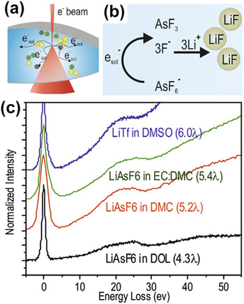
IV. ELECTRON RADIOLYSIS IN TEM TO PROBE ELECTROLYTE DEGRADATION
Electrolyte degradation in rechargeable batteries has been generally realized. However, it is difficult to directly monitor and quantify such a gradual evolution of liquid in a sealed battery. Modification of imaging electrons on the sample, or electrochemical processes in general, has been very well perceived.Reference Wang, Baer, Amonettea, Engelharda, Antony and Qiang112–Reference Grogan, Schneider, Ross and Bau115 Often, the electron-beam-induced damage or modification has to be minimized by either adjusting the accelerating voltage, reducing the electron dose, or a combination of both. Recently, Abellan et al. pioneered the concept of using electron radiolysis in TEM and STEM to study the degradation mechanism of electrolytes, as schematically illustrated in Fig. 8.Reference Abellan, Mehdi, Parent, Gu, Park, Xu, Zhang, Arslan, Zhang, Wang, Evans and Browning116 The electron beam itself caused the localized electrochemical reaction, enabling the observation of electrolyte breakdown in real time. Via in situ S/TEM, researchers explored the stability of five different electrolytes commonly used for Li-ion and Li–O2 battery applicationsReference Xu117,Reference Nasybulin, Xu, Engelhard, Nie, Burton, Cosimbescu, Gross and Zhang118 : lithium hexafluoroarsenate (LiAsF6)Reference Gofer, Ben-Zion and Aurbach119,Reference Nanjundiah, Goldman, Dominey and Koch120 ; AsF6 salt dissolved in different organic solvents, such as 1,3-dioxolane (DOL), DMC, and a mixture of DMC and EC; lithium triflate (LiTf) in dimethyl sulfoxide (DMSO) for Li–O2 batteriesReference Nasybulin, Xu, Engelhard, Nie, Burton, Cosimbescu, Gross and Zhang118; and LiPF6 in EC:DMC for Li-ion batteries.Reference Xu117 When the high-energy imaging electrons (300 kV) irradiate the solution, primary and secondary scattering occurs, generating radicals and solvated electrons. For the case of a simple salt dissolved in an aqueous solution, the electron beam essentially acts as a reducing agent, where the created radicals, such as the aqueous electrons, induce the reduction of metallic cations to grow metallic nanoparticles from the solution.Reference Belloni, Mostafavi, Remita, Marignier and Delcourt121,Reference Belloni122 In more complex solutions, such as Li battery electrolytes, the solvated electrons,  $e_{{\rm{sol}}}^ -$, and other radical species induced by the electron beam will interact through secondary chemical reactions with the salt and solvent. Figure 8 depicts an example of a likely reaction occurring between $e_{{\rm{sol}}}^ -$ and an electrolyte solution containing the salt LiAsF6. The overall reductive decomposition of the LiAsF6 electrolyte salt on carbonaceous anodes is reported to be LiAsF6 + 2e− + 2Li+ → AsF3 + 3LiF.Reference Xu117,Reference Nanjundiah, Goldman, Dominey and Koch120 Figure 8(b) illustrates both processes with the reduction reaction of AsF6− by the electron-beam-induced $e_{{\rm{sol}}}^ -$ and the subsequent recombination of F− with Li+ to form solid LiF molecules. The rate constant for the reaction of solvated electrons with AsF6− is high (K e = 9 × 10⁹ M−1 s−1), approaching values for diffusion-controlled reactions,Reference Peled, Golodnitsky, Menachem and Bar-Tow123 which indicates that AsF6− is a kinetically unstable component. Once the Lewis acid AsF3 is formed at a high rate, precipitation of LiF can occur by a simple combination of the F− anion with Li+ cation. LiF is a component frequently observed on the electrode surfaces after battery cycling in electrolytes containing fluorinated salts, such as LiAsF6 or LiPF6.Reference Verma, Maire and Novak124 Electrolytes containing the salt LiAsF6 show fast degradation under the electron beam, consistent with the high reactivity reported for LiAsF6. In addition, all three LiAsF6-based electrolytes displayed formation of nanoparticles as degradation products, which was expected due to the known formation of LiF particles from these electrolytes during previous tests.Reference Verma, Maire and Novak124 The stability of the electrolytes investigated here using in situ S/TEM correlates with electrochemical trends reported in the literature, suggesting this technique potentially could provide new insights into the reduction/degradation processes that occur during the operation of Li-ion batteries.
(a) Schematic of the interaction of imaging electrons with liquid in the liquid-cell. (b) Example of a simple process induced by electron irradiation on an electrolyte. One-electron reduction mechanism of the AsF6− component in electrolytes containing the LiAsF6 salt induced by the solvated electrons followed by possible subsequent recombination with Li+ into LiF. (c) Valence band EELS of 1 molar LiTf in DMSO, LiAsF6 in EC:DMC, LiAsF6 in DMC, and LiAsF6 in DOL. Thickness of the liquid film as a function of number of mean free paths (λ) is given for each plot.
V. EXTENSION OF IN SITU TEM TO IN SITU SEM
Based on the open-cell concept using ionic liquid electrolytes, Miller et al.Reference Miller, Proff, Wen, Abraham and Bareño66 recently developed an approach for in situ observation of cathode particles during electrochemical cycling within SEM. In Fig. 9, the fundamental concept of the device is shown by the SEM image. An electrode material was partially dipped into the ionic liquid electrolyte. To monitor the electrode's internal structure under the dynamic operating conditions of the battery, a cross-section of the electrode was cut using FIB. In a typical example, Li(Ni0.8Co0.15Al0.05)O2-based cathode materials were examined. The researchers found that significant separations develop between grains—even during the very first charge (oxide delithiation) and electrolyte penetration through that crack network all the way into the particle interior. Comparing these results to post-test microstructural characterization of oxide particles subjected to extensive cycling confirmed the occurrence of these processes in practical cells, suggesting that the physical separation and isolation of grains may contribute to performance degradation of Li-ion cells. The advantage of this cell is the large-scale observation option, which provides information on the level of electrode. The disadvantage of the device is that the ionic liquid-based electrolyte is not very relevant to the rechargeable Li-ion battery. As such, some of the electrochemical processes, such as formation of the SEI layer, may be missing.
Schematic drawing showing the fundamental concept of microscale battery for in situ study within FIB/SEM. A nanomanipulator probe was used to immerse or partially immerse an attached single cathode oxide particle into a liquid droplet covering an anode material.Reference Miller, Proff, Wen, Abraham and Bareño66

VI. SUMMARY AND PATH FORWARD
Both the open-cell and closed liquid-cell are feasible ways to probe structural and chemical evolution of materials for electrochemical applications, yet each method has its own associated advantages and disadvantages. The open-cell configuration offers the possibility of high spatial resolution imaging, but it cannot be directly correlated with electrochemical characteristics. Therefore, the open-cell is mostly suited for probing the intrinsic structural response of materials to ion insertion or extraction. Three major challenges exist for capturing high spatial resolution images using the open-cell configuration. The first one is the mechanical stability for the single nanowire system, which can be partially mitigated by using a relatively short nanowire. The second is the electron-beam-induced damage to the sample, which can be alleviated by using low-dose mode and increased detector efficiency. The third one involves orienting the sample to an appropriate zone axis as most nanomanipulators only work as a single tilt.
Development of the closed liquid-cell opens new avenues for in situ TEM study of structural and chemical evolution of electrochemical processes closely related to real working systems. Currently, for most cases, only a two-electrode system is used, and, due to the lack of the reference electrode, it often is difficult to quantitatively correlate the structural and chemical evolution with the observed electrochemical behavior. A standard three-electrode system setting for electrochemical experiments needs to be implemented. The standard electrochemical techniques, such as electrochemical impedance spectroscopy (EIS), cyclic voltammetry (CV), and chronoamperometry (CA), also need to be used. Furthermore, as a single nanowire often is used within the system, the possible involvement of peripheral material in the electrochemical process needs to be eliminated, or the surface must be passivated.
A critical contribution of the closed liquid-cell will be the observation of the SEI layers in the electrochemical system. To make this observation feasible, the following factors must be carefully considered and optimized. (1) The electron-beam-induced effects on the electrolyte need to be carefully calibrated. To eliminate possible artifacts of the electron-beam-induced electrolyte decomposition, the imaging electron dose needs to drop below the damage threshold of the electrolytes.Reference Egerton125,Reference Woehl, Jungjohann, Evans, Arslan, Ristenpart and Browning126 (2) Improving the image resolution through liquid. To obtain in situ images with high spatial resolution using organic solvent electrolytes, the thickness of the liquid layer and electron dosage needs to be optimized.Reference de Jonge, Peckys, Kremers and Piston26,Reference Woehl, Evans, Arslan, Ristenpart and Browning89,Reference de Jonge and Ross90,Reference Egerton125–Reference Welch, Faller, Evans and Browning128 The thickness of the liquid layer usually is decided by the spacer between the top and bottom chips. However, due to the liquid-induced window bulging, the liquid cell center will be much thicker than the nominal thickness. The spatial resolution drops significantly as the thickness increases, as shown in early literature.Reference de Jonge, Peckys, Kremers and Piston26,Reference Woehl, Evans, Arslan, Ristenpart and Browning89,Reference de Jonge and Ross90,Reference Jungjohann, Evans, Aguiar, Arslan and Browning127,Reference Welch, Faller, Evans and Browning128 The total SiNx-liquid thickness, t, can be estimated using EELS based on I/I 0 = e (−t/λ),Reference Egerton129 where λ is the inelastic mean free path, I 0 is the intensity of the zero-loss peak, and I is total electron intensity. This method has been used to estimate the thickness of aqueous solutions within the liquid-cell.Reference Jungjohann, Evans, Aguiar, Arslan and Browning127 Based on EELS, Holtz et al.Reference Holtz, Yu, Gao, Abruña and Muller130 mapped the liquid film thickness distribution, which clearly demonstrated that the bulging of the film increased the total thickness by a factor of 2–3. The bulging effect depends on a range of factors, such as the geometry/size of the window and film thickness. An optimized design of the window with an overall thin liquid layer ultimately will increase the image resolution. (3) The distance between the counter electrode and the working electrode needs to be shortened. In the optimized cell, the distance between the Li-source and the counter electrode should be controlled to the approximately tens of micrometer range. Thus, a more precise delivery and attachment of the Li-source electrode need to be developed within the liquid cell. One promising approach for implementing the attachment of a Li-source electrode with high accuracy is the FIB lift-out procedure.Reference Stevie, Irwin, Shofner, Brown, Drown and Giannuzzi131 Although the closed liquid-cell offers the promise of mimicking real battery behavior, the in situ cell only can be cycled for a few cycles, which is far less than the several hundred to thousand cycles of a real battery. Therefore, the structural and chemical evolution of the materials captured by the in situ cell only reflects what happens at the initial stage of battery performance. Thus, rather than expecting a long life cycle study of an electrochemical system, using the in situ cell should focus primarily on exploring the fundamental process in an electrochemical cell.
ACKNOWLEDGMENTS
The author would like to thank Meng Gu for his contribution to part of the in situ TEM studies. Most of the in situ work was carried out with support of the Assistant Secretary for Energy Efficiency and Renewable Energy, Office of Vehicle Technologies of the U.S. Department of Energy (DOE), Contract No. DE-AC02-05CH11231, Subcontract No. 6951379, under the Batteries for Advanced Transportation Technologies (BATT) Program and from the Chemical Imaging Initiative at Pacific Northwest National Laboratory (PNNL) under the Laboratory Directed Research and Development Program. The work was performed at EMSL, a national scientific user facility sponsored by the DOE's Office of Biological and Environmental Research and located at PNNL. PNNL is multi-program national laboratory operated by Battelle for the DOE under Contract DE-AC05-76RL01830. The author thanks the help of Norman Salmon and Daan Hein Alsem of Hummingbird Scientific for developing the liquid electrochemical holder that makes part of the work possible.


