


I. INTRODUCTION
Knowledge about the creep properties of metallic freestanding thin films is still scarce.Reference Wang and Prorok1–Reference Karanjgaokar, Chasiotis, Peroulis and Jonnalagadda7 This is especially true for the lower submicrometric range, due to the fragilityReference Preiß, Merle and Göken8 of the corresponding specimens, which makes their production and testing extremely challenging. This lack of data is detrimental to the design of reliable microchips and MEMS based on freestanding thin films. Mechanical creep is especially a critical issue for the radiofrequency microswitches providing essential signal processing functionalities to smartphones and other telecommunication systems.Reference Gregori and Clarke9,Reference Kolis, Bajaj and Koslowski10
The investigations presented in this publication rely on plane-strain bulge testing,Reference Xiang, Chen and Vlassak11 which is generally considered a robust method for characterizing specimens as thin as ∼40 nm.Reference Javed, Merle, Preiß, Hivet, Benedetto and Göken12,Reference Merle and Göken13 Its reliability is connected to the large area of the tested samples, which limits the statistical effects that can otherwise occur with the much smaller microtensile specimens.Reference Coulombier, Boé, Brugger, Raskin and Pardoen14 As early as 1975, bulge testing was considered suitable for creep testing purposesReference Solonovich15 and several groups have since been actively using it to investigate the time-dependent deformation of thin films.Reference Merle, Cassel and Göken16–Reference Mongkolsuttirat, Smyth, Brown and Vinci22 Some of these investigations have been performed at elevated temperaturesReference Kalkman, Verbruggen and Janssen17,Reference Ghazi and Kysar18,Reference Huang, Lu, Wu, Chen, Vinci, Brown and Lin20,Reference Mongkolsuttirat, Smyth, Brown and Vinci22 for the purpose of reproducing the operational conditions of the films used in microchips and MEMS. In this study, these technical possibilities are combined in a systematic way in order to characterize the time-dependent properties of gold thin films as a function of the applied pressure and temperature.
II. MATERIALS AND METHODS
A. Samples
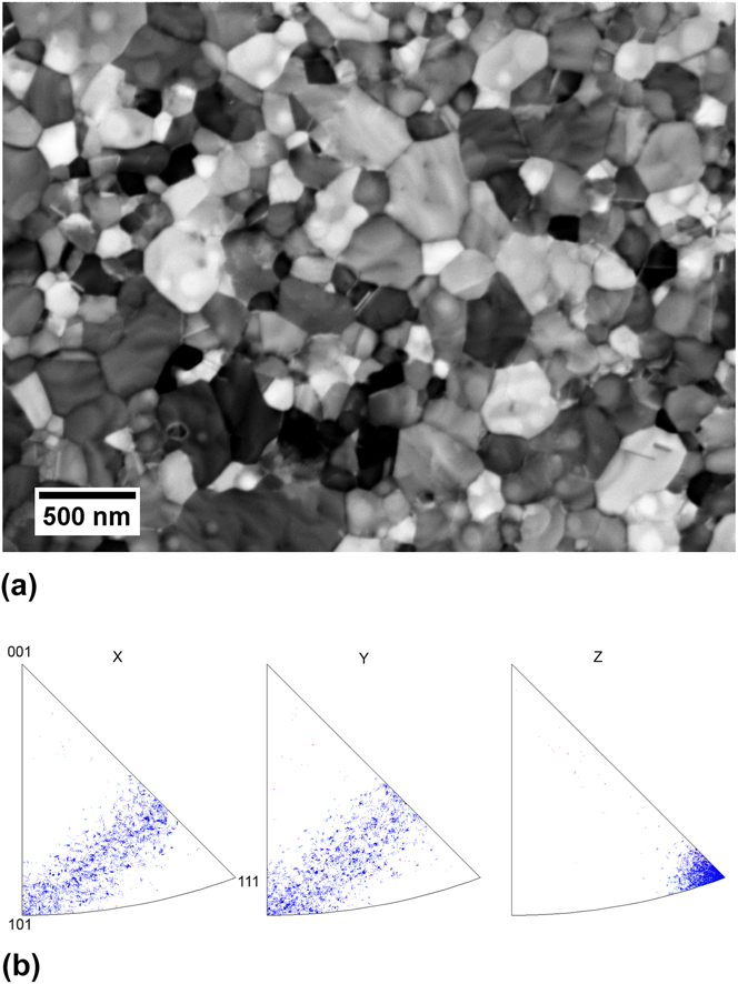
The investigated samples are 200 nm thick gold films produced by thermal deposition, using a custom built thermal coater operated at a base pressure of 2 × 10⁻⁷ mbar. Rectangular 1 mm × 4 mm SiNx membranes purchased from Silson Ltd. (Southam, U.K.) were used as sacrificial substrates. They consisted of a 100 nm thick SiNx film held by a 525 µm thick silicon frame. Gold was deposited at a rate of 1–1.5 Å/s onto the SiNx substrates while these were heated to 80 °C and constantly rotated. The substrates were preheated for 1 h prior to deposition. Following deposition, the films were heat treated at 120 °C for 2 h without interrupting the vacuum, in order to stabilize the microstructure before mechanical testing. A representative image of the resulting microstructure is shown in Fig. 1(a). An evaluation of several electron micrographs by the line intersection method evidenced a mean grain size of 220 ± 13 nm, which is slightly larger than the film thickness. This is in line with the expectation of a mostly columnar microstructure from the Grovenor deposition model.Reference Grovenor, Hentzell and Smith23 As expected for thermally grown submicron films,Reference Thompson24 the samples also evidenced a strong (111) texture, see Fig. 1(b).
Microstructure of the gold films before creep testing: (a) Back-scattered electron micrograph (CrossBeam 540, Zeiss, Germany)—(b) Inverse pole figures from EBSD (Electron Back-Scattered Diffraction, NanoLys Detector, Oxford Instruments, UK) showing a strong (111) texture.
In a further processing step, the SiNx substrate layer was removed by reactive ion etching using a 30 sccm flow of CF4 at a pressure of 12.67 Pa and a RF power of 100 W for 3 min. This left the gold film freestanding inside the 4 × 1 mm rectangular opening and ready to be mechanically deformed by bulge testing.
B. Bulge testing
The plane-strain bulge test is a convenient method for measuring the mechanical behavior of thin films. Vlassak et al. showed that the lateral stress σ and strain ε in the sample are directly related to deflection h of the membrane under the action of a given pressure pReference Xiang, Chen and Vlassak11,Reference Vlassak and Nix25 :
 $$\sigma = {{p{a^2}} \over {2ht}}\quad ,$$
 $$\varepsilon = {{2{h^2}} \over {3{a^2}}} + {\varepsilon _0}\quad .$$
The custom-built bulge tester used for this study is shown in Fig. 2. It relies on pressurization by a continuous flow of gaseous nitrogen and a measurement of the resulting deflection by white light interferometry. For the purpose of the present study, a set of miniature heater and thermocouple (Allectra GmbH, Berlin, Germany) was fitted to the sample holder and operated with a PID controller (Eurotherm, Worthing, UK). This combination ensured that the sample could be kept at any temperature in the range 23–110 °C with variations smaller than 0.1 °C during an experiment. The actual temperature of the sample was furthermore calibrated with a reference thermocouple before the beginning of the study. For the purpose of the creep tests, the bulge tester was confined inside a double-walled enclosure and left to stabilize thermally for 12 h before every creep test so that the measurements would not be affected by thermal drift due to the expansion of the setup.
Custom-built bulge tester for thin films.
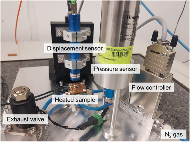
A supplementary challenge associated with bulge tests at elevated temperature is related to metallic membranes usually becoming slack when heated up, due to their thermal expansion coefficient being much larger than that of the retaining silicon frame. This is usually a critical issue for performing bulge tests because the evaluation procedure requires knowledge of the initial flat position of the membrane. Fortunately, Ghanem et al.Reference Ghanem, Göken and Merle26 have recently shown that measuring the initial height of the central buckle and subtracting it from the displacement data yields robust results, as long as the buckling is not too strong and the pattern disappears upon loading to a certain pressure, as was the case in the present study. As a consequence, the height of the buckle was measured by a line scan using the white light interferometer and its value was taken into account for setting up the creep tests and evaluating the corresponding data.
C. Creep testing
To carry out the creep tests, a feedback loop was implemented into the pre-existing Labview control program. It aimed at continuously adjusting the pressure p to keep the stress σ [Eq. (1)] equal to the value specified by the operator. This required a prior measurement of the geometrical dimensions of the sample and the height of the central buckle. The stress was held constant for a duration of 12 h, during which the load–displacement data were recorded at a rate of 5 Hz. Due to the limited availability of the samples, stress increments of at least 100 MPa were implemented so as to probe the creep response at more than one stress level for each sample and therefore maximize data collection. This procedure is commonly used in macroscopic creep testing.Reference Bauer, Neumeier, Pyczak and Göken27 On thin film samples, the repeated loading scheme was found to be unproblematic,Reference Karanjgaokar and Chasiotis28 as long as the films had been previously annealed and the stress increments were large enough. This holds true for the present study, where samples tested with and without prior stress increment experienced similar creep rates. All in all, 23 similar gold membranes were subjected to bulge creep tests.
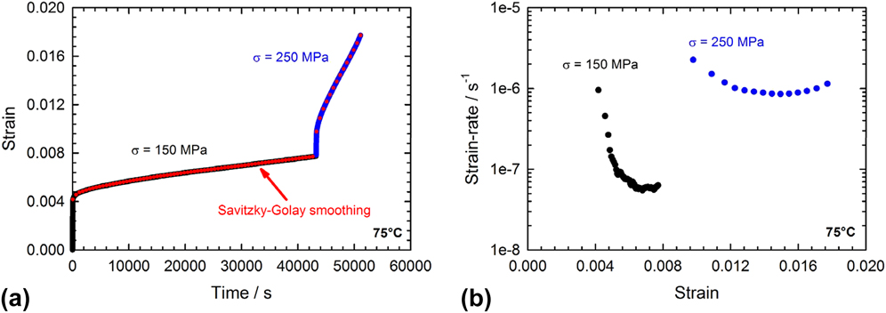
The raw load–displacement data were converted to stress–strain data using a Python/SciPy script based upon the analytical model from Vlassak et al. [Eqs. (1) and (2)]. In the next step, the strain data were smoothed and differentiated using a Savitzky–Golay numeric filterReference Savitzky and Golay29 associated to a moving window of 1200 s. The effect of the smoothing and differentiating procedures implemented in the Python/SciPy script is illustrated in Fig. 3. The outcome of a measurement is a strain-rate plot where one data point corresponds to 600 s creep data. From this plot, the minimum creep rate can be identified and used as the main parameter extracted from the creep experiment.
Smoothing of the strain data by using a Savitzky–Golay numeric filter: (a) Strain data with overlayed smoothened signal—(b) Resulting strain-rate data. The sample shattered during the creep test at 250 MPa, which is why the strain-rate increases toward the end of the measurement.
III. RESULTS
A. Apparent stress dependence
Measuring the dependence of the creep rate on the applied stress is usually an efficient way to identify the rate-limiting deformation. This is achieved by comparing the experimental values to the theoretical equations derived for most mechanisms.Reference Frost and Ashby30 The experimental data from the creep tests on the 23 specimens are displayed as Norton plots in Fig. 4(a). For each investigated temperature, the diagram describes the dependence of the creep rate on the applied stress. Within the limits of the experimental scattering, these data seem to be fairly linear within the investigated stress range. The slope of the linear regression corresponds to the apparent creep stress exponent n for this range:
 $$n = {{\partial \ln \dot{\varepsilon }} \over {\partial \ln \sigma }}\quad .$$
Apparent stress dependence of the creep of the gold films: (a) Norton plot for each tested temperature, (b) Resulting creep stress exponents as a function of the testing temperature. The error bars correspond to the bounds of the 95% confidence interval of the linear regression.
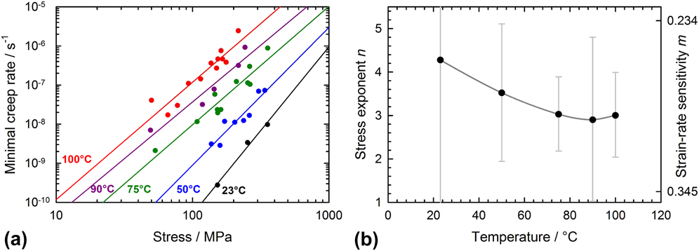
The measured stress exponents n are plotted versus the testing temperature in Fig. 4(b). Their value decreases from a maximum of 4.3 at room temperature, to a minimum of approximately 3 at 75 °C and above, which suggests a change of deformation mechanism occurring around 75 °C. However, it should be pointed out that the experimental scattering of the creep data is significant, as indicated by the large confidence intervals shown in Fig. 4(b). Most of the measured values fall within the characteristic 3–5 range of power-law creep, which is a much-investigated deformation behavior based on dislocation glide and/or climb.Reference Frost and Ashby30,Reference Weertman31
B. Apparent temperature dependence
Further information about the creep mechanisms can be inferred from the measurement of the apparent activation energy (also called Gibbs free energy). For this purpose, an Arrhenius plot has to be constructed for a given applied stress, based on the interpolated experimental data previously presented in Fig. 4(a). Calculations for 100 and 200 MPa are shown in Fig. 5. Assuming the most general activation lawReference Nabarro and De Villiers32
 $$\dot{\varepsilon } = {\dot{\varepsilon }_0} \cdot {{\rm{e}}^{ - {{U\left( \sigma \right)} \over {kT}}}}\quad ,$$
Arrhenius plots contructed from the interpolated creep data shown in Fig. 4(a) for different creep stresses: (a) 100 MPa—(b) 200 MPa. The apparent activation energy in kJ/mol is calculated by multiplying the slope by R ln 10 × 10−3.
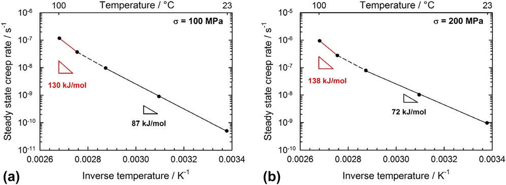
the apparent activation energy U can be calculated from the slope of the Arrhenius plots (see Fig. 5). For both investigated stress levels, it appears to remain constant between 23 and 75 °C and subsequently increases to a larger value of 130–140 kJ/mol.
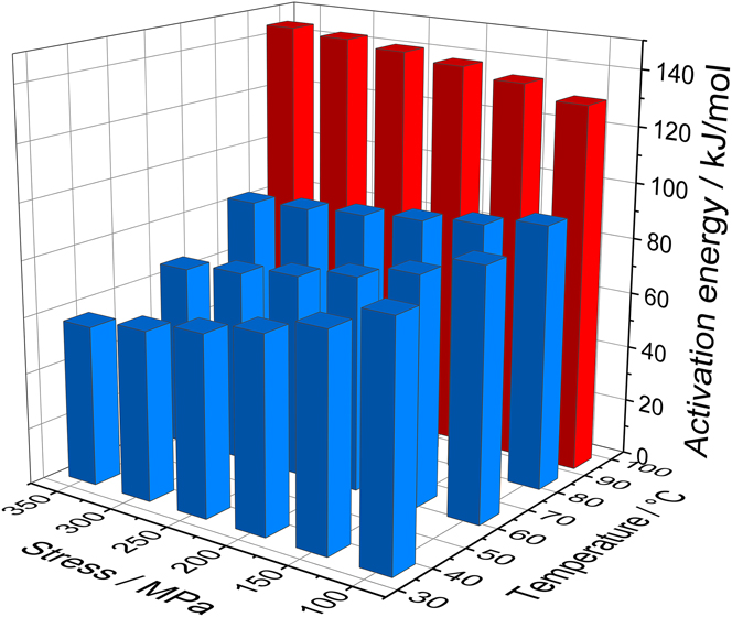
A similar analysis was performed for the whole range of investigated stresses and the corresponding apparent activation energies are summarized in Fig. 6. It is striking that the apparent activation energy depends strongly on the sample temperature and only weakly on the applied stress. This confirms the previous suggestion from the stress exponent analysis that the elevation of the temperature above 80 °C is the main driving force for a transition in deformation mechanisms. The apparent activation energy at room temperature is much smaller than the activation energy for lattice diffusion in gold (167 kJ/molReference Rupp, Ermert and Sizmann33) but on the order of grain boundary self-diffusion (85 kJ/molReference Gupta34) or surface diffusion (87 kJ/molReference Lin and Chung35). This does not conflict with the previous assumption of diffusion-assisted power-law creep at room temperature. Indeed, while power-law creep is often considered the consequence of dislocations overcoming obstacles inside the grains by climb or glide,Reference Frost and Ashby30 it has already been suggested that the annihilation of dislocation pile-ups by climb at the grain boundaries produces similar effects.Reference Nabarro36,Reference Spingarn and Nix37 In this case, the measured activation energy corresponds to the diffusion of vacancies along grain boundaries, as it is the case here. The weak dependence of the activation energy on the applied stress also visible in Fig. 6 is in no way comparable to the temperature effect. At low temperatures, its small decrease could be interpreted as an indication of the beginning of a transition to dislocation glide at higher stress levels, which is characterized by a lower apparent activation energy.Reference Gibbs38
Calculation of the apparent activation energy for the whole range of investigated stresses. A steep increase is visible around 90 °C.
The measurement of the apparent activation energy values only provides a preliminary hint at the deformation mechanism. Based on these first observations, it is necessary to compare the experimental results to the rate equations predicted by specific models available in the literature.
C. Comparison to stress activation rate-equation
The Arrhenius analysis shown in Fig. 6 hints at a strong influence of the temperature on the kinetics of creep. A popular model is often used to describe such creep deformation, which assumes that dislocations overcoming discrete obstacles by thermal activationReference Frost and Ashby30 or that the thermal activation of Frank–Read sourcesReference Nabarro and De Villiers32 is the rate-controlling process, in which case the following rate-equation should apply:
 $$\dot{\varepsilon } = {\dot{\varepsilon }_0} \cdot {{\rm{e}}^{ - {{{U_0} - V\sigma } \over {kT}}}}\quad ,$$
where U 0 is the activation energy at 0 K and V is the so-called activation volume. Given the widespread (and sometimes indiscriminate) use of this equation, it is worth taking the time to examine how well it matches the experimental data.
The first step consists of measuring the apparent activation volume as
 $$V = kT{{\partial \ln \dot{\varepsilon }} \over {\partial \sigma }}\quad .$$
This yields values of the order of b 3, which steadily increase with the testing temperature, see Fig. 7(a). However, as advocated in some textbooks,Reference Hirth and Lothe39 caution should be taken not to over-interpret the physical meaning of the activation volume and use it to identify a rate-limiting deformation mechanism. Comparison to literature values is also difficult due to the different definitions used by different researchers: V is defined as a derivative either with respect to the resolved shear stress or to the applied tensile stress [as in Eq. (6)]. In the case of a polycrystal, this leads to a difference of a factor 3.06 (Taylor factorReference Frost and Ashby30,Reference Hosford40,Reference Taylor41 ) between the different numerical values reported in the literature. Further adding to confusion, the analysis in certain publications incorrectly assumes a value of √3 for the Taylor factor, see discussion in Ref. Reference Stoller and Zinkle42. Altogether, this makes the interpretation of activation volume values and their comparison to the literature a very challenging task.
Evaluation of creep data assuming a dislocation-based discrete obstacles thermally activated limiting mechanism: (a) Activation volume (calculated with respect to σ) with 95% confidence intervals—(b) Activation energy at 0 K.
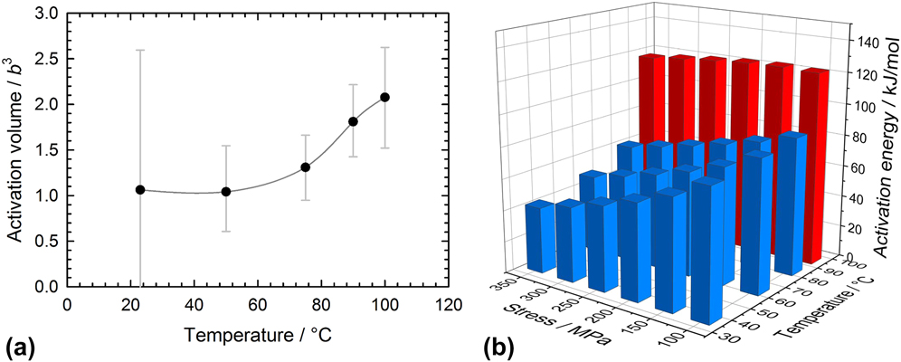
More importantly, the measurement of the activation volume enables calculating the activation energy at 0 K by subtracting the product Vσ from the previously measured [Fig. 6(b)] apparent activation energy. The new athermal values are shown in Fig. 7(b). They can readily be compared to the product μb 3 (390 kJ/mol at room temperature, with μ: shear modulus, b: Burgers vector), to gain physical information about the kind of obstacles encountered by the dislocations.Reference Hirth and Lothe30 The measured U 0/μb 3 ratio of 0.1–0.2 at room temperature is indicative of a rather weak obstacle strength. This is consistent with the fact that pure gold films do not contain precipitates.
It can be observed for any given stress that the activation energy at 0 K is strongly increased above a temperature of 80 °C. A similar trend also holds for the activation volume [see Fig. 7(a)]. The end of the stability for both parameters evidences that the discrete obstacle thermal activation model described by Eq. (5) breaks down for these temperatures. This strongly suggests that another mechanism is taking over. To characterize its nature, it is necessary to resort to direct observations of the corresponding deformation.
D. Observation of deformation
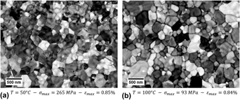
Only very few gold film specimens survived the creep tests and did not delaminate from the surface when unmounted from the bulge tester. They were inspected in electron backscattering mode (BSD), to be compared with the initial microstructure of the films (shown in Fig. 1). A few representative images taken after the creep tests are shown in Fig. 8. The mean grain size was measured by the line intersection method from at least four of such micrographs of the same sample. The measurements evidenced no significant growth during testing. For instance, for the samples presented in Fig. 8, mean grain sizes of 223 ± 13 nm and 225 ± 13 nm were found, which do not significantly differ from the pre-creep-test condition (220 ± 13 nm). This is not excessively surprising because the samples were heat treated at 120 °C prior to the tests to ensure that the microstructure would remain thermally stable. Besides, the limited strain (<1%) accumulated during the tests makes it unlikely that any very large mechanically induced grain growth takes place. However, it cannot totally be excluded that grain boundary motion takes place on a limited scale during the creep tests, which cannot be resolved due to technical limitations.
Morphology of the samples after the creep tests investigated in electron-backscattered contrast (BSD): (a) Sample tested at 50 °C—(b) Sample tested at 100 °C, with similar accumulated strains. After testing at 100 °C, prominent grooves are apparent along the grain boundaries.

Qualitatively, there appears to be a major difference between the topology of the samples shown in Fig. 8. While the sample tested at 50 °C [Fig. 8(a)] shows little differences to the microstructure pre-existing creep testing (Fig. 1), the sample tested at 100 °C [Fig. 8(b)] evidences dark bands between its grains in electron-backscattered (BSD) contrast. Closer examination reveals that these bands correspond to grooves, which amount to a local thickness reduction. This is not simply a consequence of the accumulated deformation, as both samples shown in Fig. 8 have been tested to a similar total strain. Rather, this appears to be an effect of the temperature since such prominent grain boundary grooves are only found in samples tested above 75 °C. As this temperature range correlates well with the variations in stress exponent and activation energy reported earlier, it appears likely that these are directly connected to the localization of the deformation at grain boundaries.
IV. DISCUSSION
A. Overall deformation behavior
The analysis of the data shown above allows drawing some likely conclusions about the mechanisms governing the deformation of the films at the investigated temperatures and strain-rates. At low temperatures (23–75 °C), the stress exponent analysis points toward a power-law like mechanism. The apparent activation energy value suggests that it relies on the diffusion of vacancies along grain boundaries (or surface). From this, it can be inferred that climbing of dislocations at the grain boundaries is the limiting mechanism. This is consistent with in situ TEM observations showing the annihilation of dislocations at the grain boundaries of samples of similar grain size.Reference Mompiou, Legros, Boé, Coulombier, Raskin and Pardoen43 In any case, the deformation is well described by a discrete obstacle thermal activation model up to a temperature of 75 °C.
In the high temperature range (90–100 °C), the creep data consistently suggest that another rate-controlling mechanism takes over. Although the stress exponent remains constant around 3—which could still correspond to power-law creep—there is a clear break-down from the discrete obstacles thermal activation model. Post-mortem micrographs also evidence a transition to a completely different morphology of the surface of the tested specimens, which is characterized by large grooves running along grain boundaries. The increase of the apparent activation energy to values significantly larger than for grain boundary diffusion might suggest that diffusion along grain boundaries happens much more easily, while the more demanding diffusion of vacancies from the bulk of the grains to their periphery is for some reason required and thus becomes the new rate-limiting mechanism. Deformation by pure diffusion is, however, not consistent with the measured stress exponent value (n = 1, even in the case of coatingsReference Thouless, Gupta and Harper44 versus n = 3, experimentally) and the described mechanism would presumably restrict grooving to the grain boundaries perpendicular to the main tensile direction, in opposition to the microscopic observations. This suggests that the localized deformation observed at grain boundaries is more likely connected to the accommodation of the shape of the grains required by a structural grain-boundary mediated mechanism, such as grain rotation,Reference Liu, Mao, Wang, Han and Zhang45 grain-boundary sliding,Reference Karanjgaokar and Chasiotis28,Reference Haque and Saif46,Reference Lohmiller, Kobler, Spolenak and Gruber47 or shear-coupled grain boundary migration.Reference Gianola, Van Petegem, Legros, Brandstetter, Van Swygenhoven and Hemker48–Reference Rajabzadeh, Mompiou, Legros and Combe51 It is quite true that the measured stress exponent values are slightly too high for these mechanisms, as diffusion-supported grain boundary sliding is for instance usually associated with a stress exponent n ≈ 2.Reference Lüthy, White and Sherby52 Nonetheless, it should not be overlooked that the underlying model was developed for bulk materials and neither takes into account the possible out-of-plane motion of grains in thin films nor their local thinning and their effect on the overall strain and strain-rate. It is also possible that several mechanisms almost equally contribute to the deformation so that the apparent stress dependency is in fact of a composite value.
B. Comparison to prior studies
The experimental results are partly in agreement with and partly in apparent contradiction to the limited literature available on the creep of thin films.
Karanjgaokar et al. investigated the creep of gold films in the same temperature rangeReference Karanjgaokar and Chasiotis28 as the present work and also observed a transition in deformation mechanisms. They measured similar stress exponent values (in the 3–5 range) but evidenced a different trend, with the stress exponent increasing with temperature. Hence, they concluded that the deformation shifts from grain boundary sliding at room temperature to dislocation power-law creep at 110 °C. Surprisingly, the reported apparent activation energy was found to be constant [Fig. 12(a) in Ref. Reference Karanjgaokar and Chasiotis28]. It was also significantly smaller than in the present study, suggesting that diffusion did not play any major role. It should, however, be noted that the films investigated by Karanjgaokar et al. had a very different microstructure. Not only were the films one order of magnitude thicker (t = 1.76 µm versus 200 nm) but also their mean grain size was much smaller (d = 53 nm versus 220 nm). As it is well-known from investigations on the superplastic behavior of materials that the temperature and strain-rate ranges where grain-boundary sliding occurs are significantly affected by the microstructure of the samples,Reference Feldner, Merle and Göken53 the apparent discrepancy between the studies should not be a matter of surprise.
An even finer microstructure was investigated by Ghazi et al.,Reference Ghazi and Kysar18 who performed creep tests on 200 nm thick copper films of 35 nm mean grain size at room temperature and 100 °C. In opposition to both Karanjgaokar et al. and the present study, they concluded from the experimental creep rate data that Coble creep was the dominating mechanism over the whole temperature range. The present observations agree with the importance of grain-boundary diffusion at room temperature, but the larger apparent activation energy rules it out for the tests performed at 100 °C. Besides, the exponent values measured over the whole temperature range rather point toward dislocation-based creep.
These different behaviors evidence important heterogeneities between thin films and emphasize the need for further experimental investigations of their creep behavior, so as to derive a better understanding of the effects of their microstructure.Reference Liebig, Göken, Richter, Mackovic, Przybilla, Spiecker, Pierron and Merle54 The originality of the present study lays in the strongly columnar character of its microstructure, which implies that almost every grain extends through the whole thickness. The ubiquitous presence of the free surface is known to influence the strength of the samplesReference Yang, Motz, Rester and Dehm55 and is also believed to promote grain-boundary mediated deformation because less accommodation of the neighboring grains is required. The occurrence of grain-boundary sliding has for instance already been reported in detail in a preliminary study at room temperature by the author.Reference Merle, Cassel and Göken16 The discrepancy between both room-temperature measurements most likely results from significant differences between the gold samples investigated in both studies. As a matter of fact, the earlier results were achieved on non-annealed samples, which also evidenced a much higher surface roughness, with small grain boundary grooves already present in the as-deposited condition.
V. CONCLUSIONS
All in all, the report presented a new bulge setup developed for creep tests at elevated temperatures, as well as its application to columnar 200-nm thick gold membranes. The creep data enabled the calculation of the stress exponent, apparent activation energy, and activation energy at 0 K. The recorded trends evidence a transition in deformation mechanisms occurring around 75 °C. At low temperatures (23–75 °C), deformation appears to be governed by the diffusion-assisted climb of dislocations at grain boundaries, as indicated by the stress exponent of ∼4, the value of the apparent activation energy of ∼80 kJ/mol close to grain boundaries self-diffusion and the good fit to the discrete obstacle thermal activation model. Above 75 °C, this model breaks down and the apparent activation energy increases significantly. No clear picture can be derived from the value of the creep parameters, but direct observations of the surface of the deformed samples reveal a pronounced grooving of the grain boundaries. It is therefore suggested that an increased contribution of both diffusion and grain-boundary mediated deformation is the origin of the measured changes in creep parameters. This behavior seems to be specific of the columnar microstructure investigated in the present study and is not found in thicker nanocrystalline films.
ACKNOWLEDGMENTS
The author gratefully acknowledges significant contributions by Eva Preiβ (FAU Erlangen) for building the bulge tester and by Florentina Gannott (MPL Erlangen) for RIE-etching the SiNx substrate layer below the gold films. B.M. also expresses his sincere gratitude to Jan P. Liebig for helpful discussions about the creep results.


 Open access