


Introduction
The introduction of modern silicon and especially silicon-germanium technologies, such as e.g. [Reference Böck, Aufinger, Boguth, Dahl, Knapp, Liebl, Manger, Meister, Pribil, Wursthorn, Lachner, Heinemann, Rücker, Fox, Barth, Fischer, Marschmeyer, Schmidt, Trusch and Wipf1], led to the emergence of scalable multiple-input and multiple-output (MIMO) radar systems in the D-band, especially around  $120\,\mathrm{GHz}$ and beyond [Reference Ng, Kucharski and Kissinger2–Reference Kueppers, Cetinkaya, Herschel and Pohl5].
Especially the use of automotive radars in the frequency range around  $80\,\mathrm{GHz}$ led to the development of sophisticated MIMO arrays and highly integrated measurement systems enabling the use of this technology for a multitude of other applications, like contactless vital sign detection [Reference Wang, Kueppers, Cetinkaya and Herschel6], drone detection and avoidance systems [Reference Dogru and Marques7], or imaging applications [Reference Kueppers, Herschel, Wang, Nüer and Pohl8].
Most of these MIMO systems have in common, that the local oscillator (LO) generation and distribution is separated by their respective transmitters Tx, receivers Rx, or transceivers TRX. This leads to maximum flexibility in the system design by enabling the possibility to implement a multitude of different system configurations with the same high-frequency integrated circuits (monolithic microwave integrated circuits [MMICs]). This enables the scaling of these systems from ultra-compact MIMO systems the size of a matchbox [Reference Kueppers, Cetinkaya and Pohl9], to systems with thousands of transmit and receive channels [Reference Schiessl, Genghammer, Ahmed and Schmidt10, Reference Ahmed11].
In this article, a flexible MIMO chipset is presented, consisting of different voltage-controlled oscillator (VCO) MMICs for reference signal generation, and additionally highly integrated transmitter and receiver MMICs, containing four transmitters or receivers each. For the signal generation MMICs, three different circuit implementations are investigated to determine the influence of different circuit optimization techniques on the overall performance of these VCO circuits.
In Section “Chipset concept and circuit design,” the chipset concept and the design of the individual circuits is introduced. This is followed by Section “Experimental results,” where measurement and simulation results of the implemented circuits are discussed. This article is concluded in Section “Discussion and conclusion” that not only summarizes our findings but also contains a comparison with the state-of-the-art of signal generation MMICs around  $30\,\mathrm{GHz}$ and D-band active multiplier chains.
Chipset concept and circuit design
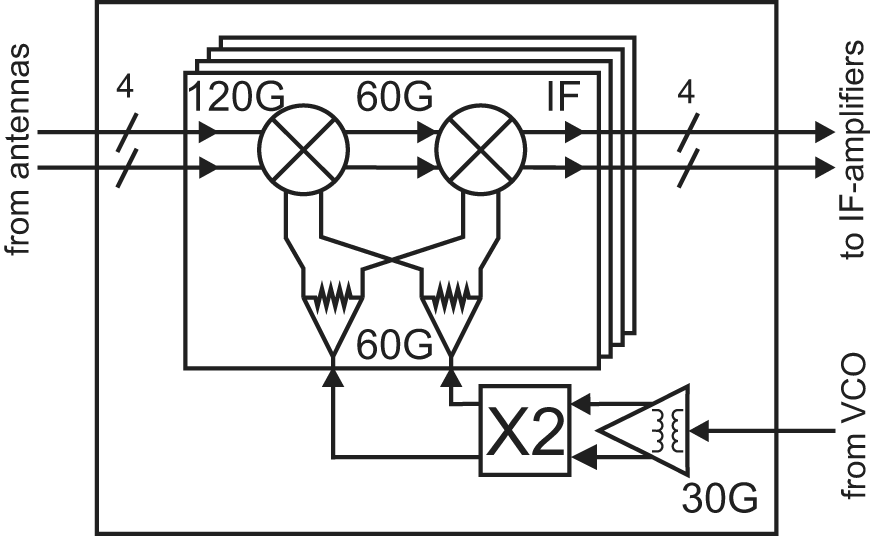
A proposed system concept for the front-end module of a  $8\times 8$ MIMO frequency-modulated continuous wave (FMCW)-radar at a center frequency of 120 GHz is shown in Fig. 1. The front-end module will be based on three different custom application-specific integrated circuits in Infineons (IFAGs) B11HFC SiGe-Technology and a frequency ramp generation block based on a custom of the shelf (COTS) phase-locked loop (PLL) chip. The PLL chip is triggered by the control logic of the backend and will stabilize a 30 GHz VCO for the generation of the frequency ramps needed for the FMCW operation of the radar. On the VCO chip, two small output amplifiers for two separate 30 GHz outputs will be realized along with a prescaler in order to use the limited input frequency range of available COTS PLL chips. The derivation of all frequency ramps from one VCO is done to provide coherence between all channels in all measurements. One of the outputs of this VCO chip is used to drive two transmit chips while the other output is used to drive the two receive chips. This coherent signal generation is done only at 30 GHz since this comparable low frequency is easier to route with less parasitic radiation than in the intended frequency band of 120 GHz. Also, a single-ended approach is used for easier distribution of the generated 30 GHz signal on the high-frequency substrate with only one metal layer.
Block diagram of a proposed 120 GHz  $8\times 8$ MIMO FMCW-radar based on the designed reference VCO, four-channel transmit and four-channel receive chip presented in this work.

The transmit as well as the receive chips integrate four channels each resulting in two transmit and two receive chips needed for the chosen  $8\times 8$ MIMO system concept. The ramp signal is pre-amplified and distributed to the four respective channels on the chips. In both chips, a frequency translation for the up-conversion of the ramp signal to the 120 GHz transmit signal and the downconversion of the 120 GHz RX input signal to the intermediate frequency (IF) ( $ \lt \!\!20\,\mathrm{MHz}$) will be realized. Quad channel MMICs have been chosen as a sweet spot for integration, chip size, still feasible bond interfaces, and inter-channel coupling. From an on-chip view, the channels are limited due to four edges that are available for distribution of bondpads on the bare die. While from a PCB routing perspective, the size and spacing between the high-frequency interfaces at 120 GHz of the MMIC and the routing to the PCB antennas already becomes quite challenging even with only four differential channels per MMIC.
The rest of this section is divided into three sub-parts describing the circuit design of the three different MMICs of the MIMO chipset used in Fig. 1. For the fabrication of the MMICs Infineon’s B11HFC [Reference Böck, Aufinger, Boguth, Dahl, Knapp, Liebl, Manger, Meister, Pribil, Wursthorn, Lachner, Heinemann, Rücker, Fox, Barth, Fischer, Marschmeyer, Schmidt, Trusch and Wipf1], automotive qualified production SiGe:C hetero bipolar technology with an  $f_{\rm{T}}$ of 250 GHz and $f_{\rm{max}}$ of 370 GHz was chosen. In addition to the high-speed heterojunction bipolar transistors (HBTs), the technology offers different flavors of HBTs (high-voltage, medium speed) and MOS transistors (digital and analog IO) in its front end of line (FEOL). Furthermore, a back end of line (BEOL) into which dedicated radio frequency (RF) metal–insulator–metal (MIM) capacitors and thin film RF-Tantalum-Nitride (TAN) resistors are integrated consisting of six copper layers and one aluminum layer, which is used for laser-fuses and pads, is offered by the manufacturer. A supply concept with only one single supply voltage of 3.3 V is used for all three SiGe MMICs.
Reference VCO MMIC
The designed reference VCO MMIC that is described here in detail and (already presented in [Reference Bredendiek, Kueppers, Aufinger and Pohl12]) offers more flexibility and features than needed for the realization of the proposed  $8\times 8$ MIMO radar given in Fig. 1. The band selection capabilities of this presented MMIC are not needed for the proposed 120 GHz system.
Block diagram of the proposed dual-band signal generation MMIC. Differential signal paths are drawn with double lines.

For the generation of the signal at the higher band, a fundamentalLC-VCO around 30 GHz is used while the lower band is generated by a frequency division by two on the chip. For stabilization within an off-the-shelf PLL chip, an additional divide-by-2 stage with a buffer is also integrated. This first sub-part is outlined in Section “Fundamental 30 GHz LC-VCO”. For the band selection, two wideband single pole, double throw (SPDT) RF switches were used due to the differential architecture which can be seen in Fig. 2. The circuit design of this second sub-part is described in Section “Wideband SPDT RF switch”. In the last Subsection “Output differential to single-ended buffer amplifier,” the design of the output unbalance buffer amplifiers that have to operate in two frequency bands simultaneously are given. These amplifiers can be enabled separately for further flexibility of the MMIC.
Fundamental 30 GHz LC-VCO
Due to its excellent efficiency and phase noise performance, a modified Colpitts–Clapp LC-VCO topology that was first presented in [Reference Pohl, Rein, Musch, Aufinger and Hausner13]. The schematic of the designed VCO is given in Fig. 3. As a result of their beneficial properties at these frequencies, all needed inductive elements ( $L_{\rm B}, L_{\rm E}$, and $L_{\rm 1}$) were realized with compact 2.5D EM simulated monolithic integrated planar inductors in the top thick metal layer of the BEOL.
Schematic of the fundamental fully differential LC-VCO at 30 GHz. All inductive elements are realized with monolithic integrated planar inductors.

The Colpitts-varactor  $C_{\rm{var1}}$ and the Clapp-varactor $C_{\rm{var2}}$ are simultaneously tuned with the same external voltage $V_{\rm{tune}}$. Here, however, no additional on-chip voltage drop for compensation of $V_{\rm BE,1}$ of transistor $\rm{T_{1}}$ is used. Although simulations have shown a decrease in tuning range by about 15%, this approach improves phase noise variation over the tuning range by about 3 dB. The oscillation tank is formed by the two varactors $C_{\rm{var1}}$ and $C_{\rm{var2}}$, the differential center-tap inductor L B, the capacitor C B, and the parasitic capacitances of $\rm{T_{1}}$.
The inductors L E are used for decoupling the oscillating tank from the resistor current source supplying  $I_{\rm{0}}$. To reduce load pull effects from the output to the oscillator an additional base-stage with transistor $\rm{T_{2}}$ is added between the load inductor $L_{\rm 1}$ and the oscillating transistor $\rm{T_{1}}$. A thorough investigation of frequency pulling as an effect of load pulling on VCOs and methods for its reduction was discussed in [Reference Pohl, Rein, Musch, Aufinger and Hausner14]. The voltage references $V_{\rm{casc}}$ and $V_{\rm{B}}$ are generated on-chip through simple diode and resistor networks from the single 3.3 V supply. The static frequency divider chain is based on current-mode-logic (CML) latches with an additional buffer behind the second divide-by-2 stage.
For further characterization, investigation and optimization purposes of the VCO, three different standalone breakout VCOs were taped out. The first one matches (VCO1) depicted in Figs. 2 and 3 with its output directly connected to the probing pads in a GSSG configuration. This breakout circuit enables an explicit estimation of load pull effects from the used divider and SPDT concept on the VCO. Within the second implementation (VCO2) custom designed deep trench areas below the spiral inductors where used. This was done to investigate a possible way to reduce eddy currents induced in the substrate below the spiral inductors, potentially increasing their quality factor. While in the third test VCO (VCO3), the core current of the VCO is regulated with a dedicated transistor degenerated current mirror as a current source instead of the simple resistor supplying  $I_{\rm{0}}$ in Fig. 3. This additional realization was chosen for optimization purposes especially regarding the temperature stability but also regarding the phase noise performance of the VCO.
Wideband SPDT RF switch
For the realization of the SPDT RF switch, all available transistor devices except for the digital MOS devices have been evaluated in simulation. The best overall results concerning insertion loss and isolation were achieved by using the high-speed HBTs available in the technology. A simple series-shunt topology is adopted for the SPDT switch which is shown in Fig. 4.
For further improvement of the series as well as the shunt devices of the SPDT, an antiparallel HBT design that was demonstrated and evaluated for the series device in [Reference Cheon, Cho, Rao, Cardoso, Connor and Cressler15] was selected. With the antiparallel design, the otherwise asymmetric HBT device can be pseudo-symmetrized.
Schematic of the wideband SPDT RF switch with a series-shunt design. Antiparallel high-speed HBTs are used to gain pseudo-symmetrical series and shunt devices.

Since the main criteria for optimizing the SPDT is the isolation between both input ports and the inactive input port to the output, with the latter one always being higher than the former one, no needed matching to  $50\,\Omega$ in favor of area savings was assumed. Also, the insertion loss of the SPDT was rebalanced for the different levels at the outputs of the VCO and the first divide-by-2 stage. This was realized by different impedance levels with the capacitors $C_{\rm 1}=100\,\rm{fF}$, $C_{\rm 2}=400\,\rm{fF}$ and resistors $R_{\rm 1}=50\,\Omega$, $R_{\rm 2}=200\,\Omega$. The switch signal SW and $\overline{SW}$ are generated on chip from a single input signal by using analog IO MOS inverters. The bases of the HBTs are terminated with a high-value resistor $R_{\rm 4}=1\,{\rm{k}}\Omega$.
Output differential to single-ended buffer amplifier
A differential-to-single-ended buffer was required, since PCB-routing of the clock tree using differential signals on a single layer is very cumbersome. Common transformer-based balun solutions at these frequencies have the drawback that the transformer only operates well either at Ku- or at Ka-Band.
Schematic of the two-stage output buffer amplifier that converts the differential signal to single-ended.

Here, a two-stage amplifier solution was used, as shown in Fig. 5. The first stage with a common differential cascode amplifier topology is responsible for the wideband amplification at Ka- as well as Ku-Band with a purely resistive load of  $R_{\mathrm L}=500\,\Omega$.
The second stage is used to transform the impedance level in order to drive a single-ended impedance of  $50\,\Omega$. A differential emitter-follower stage is used for the impedance level transformation. A current mirror load to the emitter-follower is introduced for improving the single-ended conversion at the output.
The voltage references  $V_{\rm{1}}$ and $V_{\rm{2}}$ are also generated on-chip. An additional enable-signal can be used to shut down the reference current source resulting in only small leakage current of several hundred nA as a standby current.
120 GHz four-channel transmit MMIC
This subsection describes in detail the design of the four-channel transmit MMIC that is needed for the realization of the MIMO radar system as given in the block diagram of Fig. 1. For reasons already given at the beginning of Section “Chipset concept and circuit design,” a single input frequency at one quarter of the operation frequency (30 GHz) serves as the input signal for the transmit MMICs. The single-ended or unbalanced input signal at 30 GHz is converted to a differential signal via a transformer based balun and is then pre-amplified on the MMIC before redistribution. After this signal reconditioning, the differential signal is distributed to the four receive, respective transmit channels with a passive coupler that is based on spiral inductors. The differential on-chip architecture is adopted for its various benefits such as common-mode rejection and higher usable voltage swings before transistor breakdown occurs. Every transmit chain uses its own independent quadrupler and amplifier chain to translate the input frequency from 30 GHz to the operational frequency of 120 GHz instead of one single quadrupler chain. This is done to increase the efficiency and therefore the output power since the distribution at 120 GHz would become more lossy compared to a distribution at 30 GHz. To allow for a time-division multiplexing-MIMO modulation scheme every TX-chain can be activated by separate dedicated shutdown (SHDN) or enable (EN) pins/signals.
The concepts of the developed circuits for the transmit MMIC are based on the results achieved in [Reference Kueppers, Aufinger and Pohl16] with optimizations regarding the input stage at 30 GHz and a tuning of the circuits to a center frequency of 120 GHz. In addition, the quadrupler chain from [Reference Kueppers, Aufinger and Pohl16] which consisted of two cascaded bootstrapped Gilbert cell doublers and a small output buffer was expanded by two cascaded power amplifier (PA) stages to reach higher output power levels for a higher dynamic range of the whole system. The total current consumption with one active transmit channel is 122 mA. The preamp of the MMIC is always active even when no transmit channel of the MMIC is needed to ensure a good matching of the LO input at 30 GHz. This leads to a small standby current consumption of 6.2 mA with all channels deactivated which will happen in the chosen  $8\times 8$ MIMO system proposed in Fig. 1.
60 and 120 GHz bootstrapped Gilbert doublers
One very fitting example for Gilbert cell doublers in SiGe technologies was investigated in [Reference Forstner, Starzer, Haider, Wagner and Jahn17] with the basic concept that the Gilbert cell as a mixer is multiplying two signals at the same frequency. This results in a output signal at the sum of the input frequencies as well as a DC-part. A thorough examination of the output imbalance of the supposed to be differential Gilbert cell was done in [Reference Bredendiek, Pohl, Aufinger and Bilgic18] while a comprehensive study on different doubler topologies has been done in [Reference Jaeschke, Bredendiek, Küppers and Pohl19] showing that Gilbert type doublers can deliver a good peak output power and 3 dB bandwidth at the same time. This evolution of Gilbert cell type doublers in SiGe technologies basically ended in the bootstrapped topology first described in [Reference Yuan and Schumacher20] for the implementation of the needed phase shift of the input signal to suppress the DC-part of the multiplication.
Schematic of the first bootstrapped Gilbert cell doubler used in the cascaded quadrupler.

In comparison to the common Gilbert cell doubler topology, the bootstrapped versions shows two very convenient benefits which are a higher conversion gain (CG) and a better amplitude and phase balance. The schematic of this developed and optimized doubler is shown in Fig. 6 for the first stage of the quadrupler. The bootstrapped topology employs the needed phase shift of the input signal between the input differential pair of  $\mathrm{T_{2-3}}$ and the switching quad formed by $\mathrm{T_{4-7}}$ with inductor $L_{\mathrm{1}}$ and capacitor $C_{\mathrm{1}}$.
The differences between the two cascaded doubler stages can be found in the biasing especially in the core current that is supplied with the current source of transistor  $\mathrm{T_{1}}$. This leads to a current consumption of 9.7 mA and 12.1 mA for the first and the second stage, respectively. A second difference lies within the realization of $L_{\mathrm{1}}$. In the first stage $L_{\mathrm{1}}$ is realized with a planar spiral inductor as can be seen in the chip micrograph later on. In the second stage, a transmission line has been used, due to the higher operating frequency, it can already be conveniently implemented as $L_{\mathrm{2}}$ for both stages.
120 GHz amplifiers
The three cascaded amplifiers after the quadrupler consisting of a simple buffer and two PA stages are described in this subsection. The simple buffer is used to properly decouple the PA stages from the quadrupler. While the following two PA stages consisting of an intermediate amplifier and an output amplifier are optimized to deliver a high and flat power output.
Schematic of the last amplifier in the cascaded three amplifier chain. All three amplifiers are based on the same topology with different biasing settings and matching schemes.

All three amplifiers share the same topology that is shown in Fig. 7 which is commonly used at millimeter wave frequencies. Here, a simple class-A biased cascode amplifier architecture with the differential pair  $\mathrm{T_{1}}$ as the input stage and a following base stage $\mathrm{T_{2}}$ at the output is used. To increase the gain of the amplifier, a compensation line $TL_{\mathrm{1}}$ is used between the differential pair and the base stage. While the output matching for all three amplifiers is realized with a T-type matching network formed by $TL_{\mathrm{2-4}}$. With this output network, an interstage matching between the output stage and the intermediate stage is realized resulting in less lossy networks being used. This ends up in $C_{\mathrm{1}}$ of the output stage being the exact same capacitor $C_{\mathrm{2}}$ of the intermediate stage. The same is done at the output of the last doubler and the buffer stage with $C_{\mathrm{Out}}$ in Fig. 6 being the same as $C_{\mathrm{1}}$ of the buffer in Fig. 7. This results in only the intermediate stage using a dedicated, but simple, input matching network based on transmission lines and MIM-capacitors, that is not shown here for clarity.
The class-A biasing is realized with the current source supplying  $I_{\mathrm{1}}$ which differs for the three amplifier stages. This leads to a current consumption for the buffer following the frequency translation stages of 12 mA, for the intermediate amplifier of 32 mA and the output stage of 49.7 mA.
120 GHz four-channel receive MMIC
The subharmonic four-channel receive MMIC presented in this section is based on previous work presented in [Reference Kueppers, Cetinkaya, Herschel and Pohl5, Reference Kueppers, Cetinkaya and Pohl9]. In time-division multiplexed MIMO systems with a large number of channels and high dynamic range, problems can occur due to parasitic signal radiation at the receivers. Due to limited isolation between the LO- and RF-port of the receive mixers, the LO signal with a large amplitude can directly feed into the RF input port of the mixer, where this signal will be transmitted by the receive antenna. As the receive channels of such a MIMO systems are active all of the time, the power of this parasitic transmission is multiplied by the number of channels and can cause errors in the radar measurement, like ghost targets or “smeared” targets.
To prevent these parasitic transmission signals originating at the receiver, we developed a subharmonic receiver concept, as shown in Fig. 8. In this concept, the parasitic radiation is mitigated by the introduced frequency shift of the LO signal in regard to the frequency of the received RF signal. Because of this concept, the feed-through of the LO signal is prevented by two mechanisms. Due to the frequency shift, only a  $60\,\mathrm{GHz}$ differential signal or a $120\,\mathrm{GHz}$ common-mode signal can occur at the RF port of the first mixer. Due to the geometric configuration of the intended differential receive antennas, neither signal can be radiated from the antennas, as the antenna can not radiate common-mode signals and the length and width of the antenna is optimized for a center frequency of $120\,\mathrm{GHz}$ and therefore too short to radiate a $60\,\mathrm{GHz}$ signal. Furthermore, due to the differential characteristic of the mixers, the common-mode signal at $120\,\mathrm{GHz}$ is attenuated by the common-mode rejection of the current source.
In this receiver implementation, we use a single-ended input signal at a center frequency of  $30\,\mathrm{GHz}$ and convert this signal to a differential signal using a balun and a preamp circuit, similar to [Reference Kueppers, Cetinkaya, Herschel and Pohl5]. This signal is doubled in frequency and amplified before it is split for distribution on the receive MMIC. The individual receivers consist of two cascaded mixers operating at one half of the $120\,\mathrm{GHz}$ input frequency, therefore the input signal at a frequency of $120\,\mathrm{GHz}$ is down-converted to a first IF of $60\,\mathrm{GHz}$ and then in a second step converted again to an IF in the baseband.
Block diagram of the developed subharmonic receiver MMIC.
LO input and distribution network
For the LO input and distribution network on the receive MMIC circuits derived from [Reference Kueppers, Aufinger and Pohl16] are used. In the presented receiver MMIC, we use the input balun, preamp, and first frequency doubler cell to generate the differential, subharmonic LO signal. Instead of the frequency quadrupler presented in [Reference Kueppers, Aufinger and Pohl16], we omitted the second frequency doubler to generate a subharmonic LO signal for this receiver implementation.
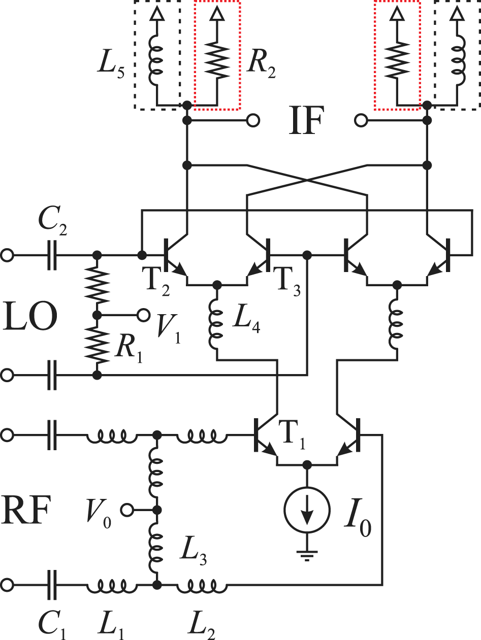
Receive mixers
The two downconversion mixers of this receiver architecture are based on Gilbert cell mixers. The schematic of the mixers is depicted in Fig. 9. The difference between the first and second mixer stage lies in the used load impedance, the current source I 0, and the reference voltages V 0 and V 1. As the first mixer stage has a output frequency around  $60\,\mathrm{GHz}$ an inductive load impedance can be used (as depicted in the black dashed boxes). This solution has the advantage, that the inductive load exhibits minimal dc voltage drop, therefore, more voltage headroom is available for the output signal. This available headroom is used to implement a degenerated current mirror as the current source I 0, to ensure high common-mode rejection for the first mixer stage. In return, the voltage drop over the base-emitter diode of the current source leads to a voltage difference of $\approx 800\,\mathrm{mV}$ for the bias voltages $V_\mathrm{0}$ and $V_\mathrm{1}$ compared to a resistor current source.
The second downconversion mixer converts the  $60\,\mathrm{GHz}$ signal into a baseband signal, therefore a resistive load impedance (as depicted in the red dotted boxes) is used in this mixer implementation. Due to the voltage drop introduced by this resistive load impedance, we use a resistive current source for the second mixer stage.
To complement the two receive mixers an additional differential IF amplifier is implemented for each of the receive channels on the receiver MMIC. This IF amplifier is connected with signal pads to anti-aliasing filters on the front-end PCB of a radar system.
Schematic of the implemented downconversion mixers. For the first mixer stage, a inductive load (black dashed box) is used, the second mixer stage uses a resistive load (red dotted box).
Experimental results
Reference VCO MMIC results
The fabricated MMIC measures  $0.86\rm{\,mm}^2$ in size and is shown in Fig. 10. The on-wafer measurements were conducted with a Rohde & Schwarz FSW85 spectrum analyzer and a Rohde & Schwarz NRP power meter. Losses of the probes and cables were de-embedded. The two separate outputs on opposite sides to the left and right are chosen for a high level of flexibility and routing options on PCB level. The total measured power consumption of the chip is 212 mW from the 3.3 V supply. This divides into 52.8 mW VCO, $2\times43.8$ mW for the buffer amplifiers, $2\times9.7$ mW for the SPDT, and 52.2 mW for the frequency divider.
Photograph of the dual-band MMIC with highlighted building blocks. The overall chip size is  $930 \times 930$ $\mu \mathrm{m}^{2}$ which is mainly dominated by the VCO and its planar inductors.

As a first measurement result the tuning curves of the two bands are shown in Fig. 11. Both tuning curves agree very well with each other with half of the absolute tuning range at one-half of the center frequency. The relative frequency tuning range of both bands is the same with 32%.
Measured oscillation frequency versus tuning voltage of the MMIC chips at room temperature for both bands. The center frequency as well as the tuning range are perfectly halved for the lower band.

As a second result, the output power achieved by this MMIC at one of its two outputs is plotted in Fig. 12. The output levels at both frequency bands are nearly on the same level even though the fundamental VCO can easily deliver much higher levels than the first divide-by-2 CML stage. To further balance the levels of both bands, a buffer between the first and second divider stage could be introduced in a future work. For this work, an important result is the observable feed-through of the feed-through of the unwanted harmonic. The suppression of the unwanted signal is better than 25 dB in all cases. The feed-through of the Ka-Band is more problematic due to the decreasing but expected isolation of SPDTs with frequency. The output power levels of more than −10 dBm are large enough to be distributed to an array of RX- and TX-SiGe-MMICs with built-in active baluns or buffers.
Measured output power  $\rm P_{Out}$ at one output versus frequency for both bands. The high isolation of the SPDT can be observed with suppression of the feed through.

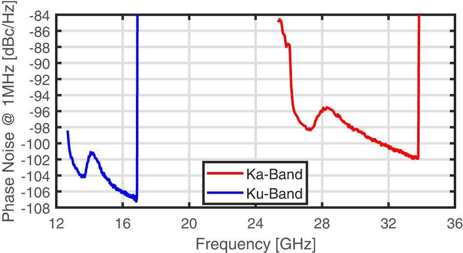
Lastly, the phase noise in both bands is plotted over the oscillation frequency at 1 MHz offset in Fig 13. The strong rise in phase noise at the band edges is due to the limits of the varactor. At the upper edge, the avalanche breakdown occurs while at the lower edge the varactor begins to be biased in forward region. The phase noise minimum is −101.9 dBc/Hz and −107.2 dBc/Hz for the Ka- and Ku-Band, respectively. This results in a minor decrease of 5.3 dB for the Ku-Band from the expected 6.02 dB from an ideal frequency translation by 2. This small sub-dB difference between the two switching states can also be seen in simulations but on a still smaller scale. The unfavorable effects of the chosen switch and divider architecture as a load on the VCO can also be seen with the available breakout chips of the VCO which are shown in the following Subsection “Standalone 30 GHz VCO results”. The phase noise variation stays within 6 dB when neglecting the steep edges at the limits of the varactor.
Measured phase noise versus frequency for the two bands. The results are in good agreement with the expected phase noise change of 6.02 dB due to the frequency translation.
Standalone 30 GHz VCO results
All three different standalone implementations of the VCOs where characterized on-wafer. The results for VCO2, the design with the additional deep trench areas below the planar spiral inductors, however, shows very small improvements compared to the original VCO (VCO1). Therefore, the results for VCO2 are not shown here for a clearer arrangement of the achieved results.
From a tuning range perspective, all three VCOs show nearly the same performance with marginally differences. The center frequencies fC are 30.29, 30.23, and 30.17 GHz with frequency tuning ranges of 10.05 (rFTR = 33.18%), 9.97 (rFTR = 32.98%), and 10.1 GHz (rFTR = 33.48%) for VCO1, VCO2, and VCO3, respectively. This also matches very well to the result achieved in the reference VCO MMIC shown in Fig. 11.
The DC current consumption of VCO3, the one VCO with a dedicated current source, on the other hand shows a stronger difference to the other two implementations with the simple resistor as a current source. While VCO1 and VCO2 consume a measured current of 16 mA in total, VCO3 only consumes 13 mA in total. This is counter intuitive since VCO3 consumes an additional biasing current for the current source and therefore a higher current consumption was expected. The higher current consumption can be explained by a rectifying process through the occurring oscillation at the base nodes of  $T_{\mathrm{1}}$ which increases the common mode potential $V_{\mathrm{B}}$. This behavior can also be reconstructed within simulations, which leads to a higher current consumption for VCO1 and VCO2 since the current consumption is directly and strongly correlated to the voltage drop over the current source. While the degenerated transistor current source in VCO3, which has a similar topology than the current source used in the frequency doubler in Fig. 6, shows a comparatively low dependency on this voltage deviation. The temperature stability for VCO3 is also much better with an increase of only 0.3 mA ( $+2.3\%$) with an temperature increase of 75 $^\circ\mathrm{C}$ (from room temperature at 25 $^\circ\mathrm{C}$ to 100 $^\circ\mathrm{C}$). Compared to 1 mA ( $+6.25\%$) for VCO1 and VCO2 for the same temperature change. Furthermore, the current consumption of VCO1 and VCO2 are also depended on the tuning voltage which will be seen and explained later on.
Measured phase noise versus frequency for VCO1 and VCO3 at room temperature (25 $^\circ\mathrm{C}$) and an elevated temperature of 100 $^\circ\mathrm{C}$.

Due to this variance in  $I_{\mathrm{0}}$, a higher impact on the phase noise as well as the output power is to be expected. This influence and large difference can clearly be seen in the measured phase noise of VCO1 and VCO3 shown in Fig. 14. From Fig. 14 can be observed that for high frequencies between 32 and 34 GHz the phase noise level is dominated by the contribution of $I_{\mathrm{0}}$ and therefore the current densities of the oscillating HBTs $\mathrm{T_{1}}$ with a phase noise level of about −120 dBc/Hz for VCO3 compared to −114 dBc/Hz for VCO1 where a higher $I_{\mathrm{0}}$ is applied. While the frequency opposing trend can be explained by the quality factor of the LC-tank where the quality factor of the pn-varactor is decreasing with its applied junction voltage through $V_{\mathrm{tune}}$. The mean phase noise level of VCO2 for a frequency range from 32 to 34 GHz is only about 0.5 dB better than for VCO1 (VCO1: −113.61 dBc/Hz, VCO2: −114.13 dBc/Hz). In retrospect two versions of VCO3 with the different spiral inductor implementations would have been the better approach to properly gauge the influence of the deep trench areas due to the higher impact of the LC-tank quality factor on the lowest noise floor level of the VCOs.
Compared to the results of the reference VCO MMIC from Subsection “Reference VCO MMIC results,” the phase noise is much better when loaded by the  $50\,\Omega$ interface of the measurement equipment than, as already mentioned in Subsection “Reference VCO MMIC results,” the unfavorable load of the divider and the SPDTs on the VCO. The difference for the same VCO just at different load conditions at 34 GHz is 12 dB worse when comparing Fig. 13 to Fig. 14. Another interesting point that can be observed in Fig. 14 as well as in Fig. 13 is the hump near 28 GHz which does exclusively not appear in VCO3. This hump relates to the previously stated dependency of the current consumption of VCO1 and VCO2 from the tuning voltage. At lower tuning voltages the high oscillation amplitudes are alternately turning the diodes of the differential pn-varactor into forward region. This effectively clips the oscillation amplitude in the core which leads to a current starvation of $I_{\mathrm{0}}$ for VCO1/2. This roughly starts to occur for $V_{\mathrm{tune}}$ below 1.5 V. Since this effect is anti-proportional to $V_{\mathrm{tune}}$ $I_{\mathrm{0}}$ for VCO1/2 and therefore also the phase noise level converges to that of VCO3.
From a output power focus, the higher consumed current for VCO1 and VCO2 is beneficial. The 3 mA higher core current  $I_{\mathrm{0}}$ also leads to a higher peak output power for VCO1 and VCO2 of −1 dBm around 30 GHz. The better regulated $I_{\mathrm{0}}$ within VCO3 on the other hand leads to a better flatness over frequency but at a maximum output power level of −4 dBm. But, from this it is also clearly evident that the DC-to-RF-efficiency for the Class-B biased VCO1 and VCO2 is better with 15% compared to the Class-A biased 9.3% of VCO3. With an external tuning pin, the reference current of the current mirror can be controlled which allows for an additional adjustment of the output power of $I_{\mathrm{0}}$ for VCO3. With an increase of the total current consumption to 15.3 mA, the peak output power for VCO3 is increased by 2 dBm but at the same time the minimum phase noise level of VCO3 is also increased by about 2 dB.
120 GHz TX SiGe MMIC results
Chip-photo of the developed four-channel transmitter. The overall chip size of the receiver MMIC is  $3000 \times 1448$ $\mu{\mathrm m^{2}}$.

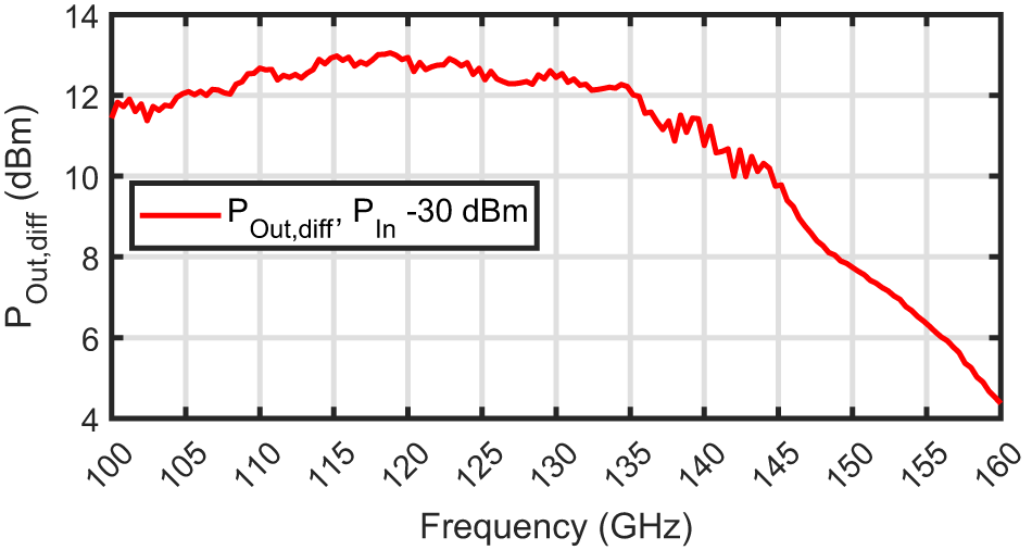
The chip-photo of the 4 channel 120 GHz transmit MMIC is shown in Figure 15. The frequency response of one channel is shown in Fig. 16 as a first result. To obtain this result, an input signal is applied by a Keysight PSG signal generator and its frequency is swept from 25 GHz up to 40 GHz at a constant input power level of  $\rm P_{In}=-30\,dBm$. The losses at 120 GHz have been perfectly compensated by vector network analyzer measurements while at higher frequencies more losses especially from the coaxial cable have not been properly compensated. Still the variation over frequency between 100 and 145 GHz is below 3 dB, which is a very good result. Additionally, it is important to note that the used measurement equipment (GGB Dual GSGSG 145 GHz Probe and Anritsu 0.8mm semi rigid coaxial cable) are only certified up to 145 GHz. Due to this, the measurement above 145 GHz is not valid. The actual performance above 145 GHz is expected to be even better than the measured result shown in Fig. 16. Even with these constraints from the measurement it is clear that the half-power bandwidth of the transmitter chip is larger than the available tuning range of the VCO MMIC.
Measured differential output power  $\rm P_{Out,diff}$ at one output channel versus frequency at a constant input power of $\rm P_{In}=-30\,dBm$.
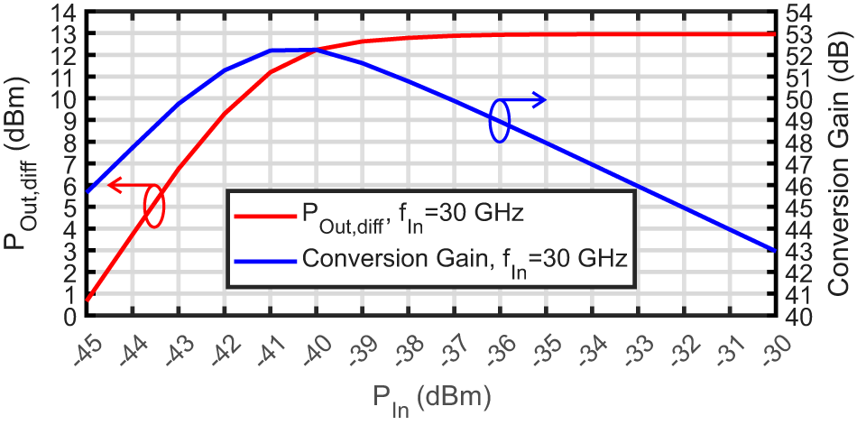
As a second result, the compression performance of the transmit chain is shown in Fig. 17. For this measurement, the input signal from the signal generator was fixed at 30 GHz while its power level was swept from −45 to  $\rm -30\,dBm$. As can be seen from Fig. 17, an input power level of $\rm P_{In}=-30\,dBm$ at the input pad of the chip is enough to fully saturate the transmit chain. This can be attributed to the preamp that is used as an active balun as the first stage. This is very important to reduce the impact of variations from the distribution network. The maximum output power of about 12.9 dBm is already obtained at input power levels of $\rm P_{In}=-36\,dBm$ and this level is kept even at input levels as high as $\rm P_{In}=-10\,dBm$. This result also clarifies the previously made assumption in Section “Reference VCO MMIC” that the minimum output power of −10 dBm at the high band of the reference VCO MMIC is high enough to drive the transmit and receive chip even after passive distribution on a PCB. The CG of the active multiplier chain is as high as 52 dB at for instance 120 GHz and an input power of −40 dBm.
Measured differential output power  $\rm P_{Out,diff}$ and conversion gain at one output channel versus input power $\rm P_{In}$ at an input frequency $\rm P_{In}=30\,GHz$.
120 GHz RX SiGe MMIC results
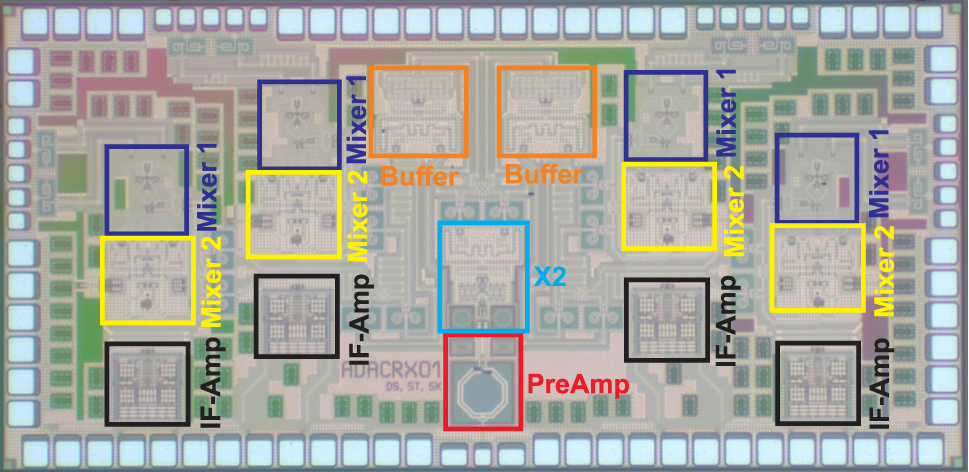
The circuit layout of the developed four-channel subharmonic receiver MMIC can be seen in Fig. 18. In this figure, the general layout of this receiver chip can be distinguished. The single-ended LO input at a frequency of around  $30\,\mathrm{GHz}$ is located at the bottom center. This external single-ended signal is converted to a differential signal and amplified by a preamp circuit (PreAmp) and then frequency doubled by a doubler circuit (X2). The differential $60\,\mathrm{GHz}$ LO signal is then split and amplified by the buffers shown in Fig. 18. The signals is then split again for distribution to the four individual receive channels, consisting of two mixers (Mixer 1 & Mixer 2) and one IF amplifier (IF-Amp) each. The $120\,\mathrm{GHz}$ RF inputs of the receivers are distributed along the top half of the MMIC. Due to space constraints, the inputs of the leftmost and rightmost receiver are placed on the left and right edge of the chip. The low-frequency outputs of the IF amplifiers are connected to the pads on the bottom edge of this MMIC.
Chip-photo of the developed subharmonic four-channel receiver.The overall chip size of the receiver MMIC is  $3000 \times 1448$ $\mu{\mathrm m^{2}}$.
Due to this compact and highly integrated layout and the resulting complex contact configuration, the characterization of this MMIC was challenging, as this receiver was not intended to be measured on a on-wafer measurement setup, but characterized based on the overall system performance. Because of the pad configuration, that made the characterization of the MMIC infeasible using only on-wafer probes, we chose to perform the measurement of this chip using a combination of on-wafer probes and integration on a measurement PCB. Using this PCB, the power supply and low-frequency IF-signals of the MMIC are bonded to the PCB and are connected to connectors for characterization. This enabled the characterization of the MMIC using only two RF probes for the measurement, a 27.5– $32.5\,\mathrm{GHz}$ input signal for the LO generation and a 110– $130\,\mathrm{GHz}$ signal as an artificial receive signal for characterization. A photograph of the used measurement setup is depicted in Fig. 19. On the right of this figure, a $170\,\mathrm{GHz}$ GSG probe is depicted that is used to connect the artificial receive signal at frequencies between 110 and $130\,\mathrm{GHz}$, which are generated using a Keysight PSG signal generator and a VDI VNA-X frequency extender module. On the left of this figure, a $40\,\mathrm{GHz}$ GSG probe is used to feed the chip with an LO signal with a frequency between 27.5 and $32.5\,\mathrm{GHz}$ with a power level of $-6\,\mathrm{dBm}$. The IF signals of the receiver are connected to SMA connectors, which are soldered to the underside of the PCB below the $40\,\mathrm{GHz}$ probe. These signals are connected to a Keysight Infiniium mixed-signal oscilloscope for characterization of the IF signal. The dc supply is connected on the bottom of the figure with a pin-header that leads to traces which are bonded to the supply pads of the MMIC.
Photograph of the used measurement setup for characterization of the four-channel receiver MMICs. High-frequency signals at 30 and  $120\,\mathrm{GHz}$ are fed to the MMIC with on-wafer probes while dc and IF signals are bonded to the measurement PCB.

In Fig. 20, the results of small-signal measurements and simulations of the developed circuits are detailed. Measurements as well as simulations were performed with a RF input power of  $\approx -22\,\mathrm{dBm}$ and an IF frequency of $25\,\mathrm{MHz}$. Because of mechanical incompatibilities of the available D-band noise source with this measurement setup, noise measurements could not be performed, but simulations of the noise figure (NF) of the receiver were done with the highest accuracy possible. For these simulations, a simulation model containing parasitic resistors and capacitors, introduced by the circuit layout, were included and the simulations were performed utilizing HICUM transistor models at a temperature of $80^\circ\mathrm{C}$. In this figure, the CG and integrated NF of the subharmonic receiver circuit, implemented by two mixer cells and an IF amplifier, are depicted for input frequencies between $110\,\mathrm{GHz}$ and $130\,\mathrm{GHz}$. A CG between $22.59\,\mathrm{dB}$ and $29.3\,\mathrm{dB}$ and an NF between $12.99\,\mathrm{dB}$ and $17.67\,\mathrm{dB}$ can be evaluated for this frequency range.
Measured conversion gain (CG) and simulated noise figure (NF) of the implemented subharmonic receiver MMIC for different input frequencies.

To investigate the large signal behavior of the developed receiver architecture, the output signal of the circuit was characterized while performing a power sweep for the artificial receive signal. For this measurement, the conversion gain CG and differential output voltage  $\mathrm{V_{Out,diff}}$ of the developed circuit was investigated for different input powers $\mathrm{P_{In}}$. To perform this measurement, the output power of the used VNA-X frequency extender, that is generating the artificial receive signal, is characterized using a Erickson PM5B power meter for more than 50 settings of the internal mechanical attenuator, achieving output powers between −25 and $+10\,\mathrm{dBm}$. As the simulated compression point at center frequency is around $-20\,\mathrm{dBm}$, an additional fixed $30.4\,\mathrm{dB}$ rectangular waveguide attenuator was utilized, to achieve output powers as low as $-45\,\mathrm{dBm}$. Using this characterized signal source, the output voltage and CG for input powers between −45 and $+5\,\mathrm{dBm}$ was evaluated. The results of this measurements are shown in Fig. 21 for an input frequency of $120.025\,\mathrm{GHz}$ and an LO frequency of $30\,\mathrm{GHz}$, resulting in an IF frequency of $25\,\mathrm{MHz}$. Here a CG between 27 and $30.5\,\mathrm{dB}$ can be evaluated for input powers between −45 and $-22\,\mathrm{dBm}$. The maximum differential output voltage in this region is achieved at an input power of $-21.4\,\mathrm{dBm}$, resulting in a differential output voltage of $1.82\,\mathrm{V}$ peak-to-peak ( $-3.83\,\mathrm{dBV}$). For higher input powers, the receiver is in saturation, resulting a linear decrease in CG and only a marginal increase in output voltage with a maximum output voltage of $2\,\mathrm{Vpp}$ ( $-3\,\mathrm{dBV}$) at an input power of $5\,\mathrm{dBm}$.
Measured conversion gain and differential output voltage of the subharmonic receiver at center frequency for different receive powers  $\mathrm{P_{In}}$.

To characterize the needed LO input power of the receiver chip, we varied the LO power from the level of  $-6\,\mathrm{dBm}$, as stated in the description of the earlier receiver measurements, down to $-30\,\mathrm{dBm}$. While performing this measurement no perceivable degradation in receiver performance could be observed. This is due to the high gain of the preamplifier and the frequency conversion stage integrated into the LO distribution network on the MMIC.
The measured current consumption of one 4-channel receiver MMIC is  $157.1\,\mathrm{mA}$ from a $3.3\,\mathrm{V}$ supply voltage, resulting in a power consumption of $518.4\,\mathrm{mW}$ per receiver MMIC.
Discussion and conclusion
This paper presents a 120 GHz SiGe MMIC chipset developed with scale-able FMCW MIMO radar systems in mind. The chipset consists of three different MMICs. The first MMIC introduces a clever and flexible signal generation solution for the distribution of the LO signal in a tree hierarchy at Ka- and Ku-Band. The concept is based on multiplexing a fundamental signal at 30 GHz with a frequency by 2 divided signal at 15 GHz over HBT-based SPDTs with high isolation. A wideband output buffer supplies output levels of more than −10 dBm with an additional conversion from differential to single-ended signals over a wide relative tuning range of 32%. This MMIC can directly be used to implement MIMO radar systems at 15 or 30 GHz as well as indirectly as is showcased with this paper.
To compare the shown results of the first MMIC and the breakout VCOs in a fair way for oscillators in Table 1, we used the  $\rm{FoM_{VCO-PAT}}$ defined in [Reference Jaeschke, Bredendiek, Küppers and Pohl19]. A focus in this comparison was put onto ultra-wideband VCO topologies around 30 GHz. This defined figure of merit (FoM) factors every key performance element and is based on the three FoMs defined by the ITRS. It is defined as
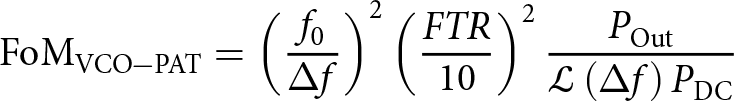 \begin{equation}
{\rm FoM_{VCO-PAT}} = \left(\frac{f_{0}}{\Delta f}\right)^{2}\left(\frac{FTR}{10}\right)^{2}\frac{P_{{\rm Out}}}{\mathcal{L}\left(\Delta f\right)P_{{\rm DC}}}
\end{equation}
\begin{equation}
{\rm FoM_{VCO-PAT}} = \left(\frac{f_{0}}{\Delta f}\right)^{2}\left(\frac{FTR}{10}\right)^{2}\frac{P_{{\rm Out}}}{\mathcal{L}\left(\Delta f\right)P_{{\rm DC}}}
\end{equation} with f 0 the center frequency,  $\Delta f$ the offset frequency at which the phase noise $\mathcal{L}\left(\Delta f\right)$ is taken, FTR the relative frequency tuning range in percent, $P_{{\rm Out}}$ the output power of the signal source, and $P_{{\rm DC}}$ the power consumption of the signal source. Based on this $\rm{FoM_{VCO-PAT}}$, the here presented VCO3 shows to the best of the authors knowledge the best overall performance for VCOs at a center frequency of 30 GHz.
Performance summary of the VCOs and comparison to the state-of-the-art

The second MMIC is a four-channel transmit MMIC based on quadruplers and amplifiers to supply a high output power over a wide frequency range. The achieved results of the implemented active multiplier chains is thoroughly compared to the state-of-the-art in Table 2. Even though significant measurements are limited to a frequency range of 100–145 GHz, the multiplier chains shows very good results regarding the 3 dB bandwidth and output power. A peak output power of 12.9 dBm with half-power bandwidth of more than 45 GHz could be demonstrated which competes very well with the shown state-of-the-art. But, it also shows that the already large tuning range of the VCO is not enough to fully use the potential of the transmit MMIC bandwidth wise.
Performance summary of the wideband D-band active multiplier chain and comparison to the state-of-the-art

The last MMIC of the chipset is the four channel receive MMIC. This MMIC implements a uncommon sub-harmonic approach to suppress a unwanted LO-to-RF feed-through at 120 GHz. This architecture shows a measured CG as high as 29 dB in the intended frequency range from 117 to 122 GHz with a at least simulated minimum NF as low as 13 dB at 110 GHz.
The presented three MMIC chipset provides a very promising starting point for scale-able MIMO radars. The achieved results from all three MMICs are expected to be sufficient for demonstration in a radar system. The next steps include the realization, demonstration, and characterization of a  $8\times 8$ MIMO FMCW radar systems in our future work.
Acknowledgements
This project has received funding from the ECSEL Joint Undertaking (JU) under grant agreement No 876019. The JU receives support from the European Union’s Horizon 2020 research and innovation program and Germany, Netherlands, Austria, Romania, France, Sweden, Cyprus, Greece, Lithuania, Portugal, Italy, Finland, and Turkey. The authors would also like to thank Infineon Technologies AG and its staff members for fabricating the chips.
Competing interests
The author(s) declare none.

Christian Bredendiek was born in Gelsenkirchen, Germany, in 1981. He received the Dipl.Ing. and Dr. Ing. degrees in electrical engineering from Ruhr University Bochum, Bochum, Germany, in 2008 and 2014, respectively.
From 2008 to 2014, he was a Research Assistant with the Institute of Integrated Systems, Ruhr University Bochum. Since 2015, he has been with the Department of Integrated Circuits and Sensor Systems, Fraunhofer Institute for High Frequency Physics and Radar Techniques FHR, Wachtberg, Germany. His current research interests include frequency synthesis, working on system concepts, and integrated circuits for various mm-wave applications.
Dr. Bredendiek was a recipient of the EuMIC Best Paper Award from European Microwave Week in 2012 and a co-recipient of the EuMIC 2021 Best Student Paper Award.

David Starke was born in Herne, Germany, in 1992. He received the B.Sc and M.Sc. degrees in electrical engineering and information technology from Ruhr University Bochum, Bochum, Germany in 2015 and 2017, respectively.
Since 2017, he has been a Research Assistant with the Institute of Integrated Systems, Ruhr University Bochum, Bochum, Germany.
His current research interests include mm-wave to THz radars and monolithic microwave integrated circuit (MMIC) design using silicon-germanium technologies.

Simon Kueppers was born in Oberhausen, Germany, in 1988. He received the M.Sc. degree in electrical engineering from Ruhr University Bochum, Bochum, Germany, in 2014, where he is currently pursuing the Ph.D. degree in system architectures for MIMO radar systems. In 2015, he joined the Fraunhofer Institute for High-Frequency Physics and Radar Techniques FHR, Wachtberg, Germany, where he was involved in the research on system architectures for millimeter-wave MIMO radar systems. He is currently Chief Technology Officer with 2 ${\pi}$ LABS GmbH, Bochum.

Klaus Aufinger was born in Kirchbichl, Austria, in 1966. He received the diploma and the Ph. D. degrees in physics from the University of Innsbruck, Austria, in 1990 and 2001, respectively. In 1991, he joined the Corporate Research and Development of Siemens AG, Munich, Germany, where he investigated noise in submicron bipolar transistors. Now he is with Infineon Technologies, the former semiconductor group of Siemens, Munich, working in the field of device physics, technology development and modeling of advanced SiGe technologies for high-speed digital and analog circuits.

Nils Pohl received the Dipl.-Ing. and Dr.-Ing. degrees in electrical engineering from Ruhr University Bochum, Bochum, Germany, in 2005 and 2010, respectively.
From 2006 to 2011, he was a Research Assistant with Ruhr University Bochum, where he was involved in integrated circuits for millimeter-wave (mm-wave) radar applications. In 2011, he became an Assistant Professor with Ruhr University Bochum. In 2013, he became the Head of the Department of mm-wave radar and high frequency sensors with the Fraunhofer Institute for High Frequency Physics and Radar Techniques, Wachtberg, Germany. In 2016, he became a Full Professor of integrated systems with Ruhr University Bochum. He has authored or coauthored more than 200 scientific papers and has issued several patents. His current research interests include ultra-wideband mm-wave radar, design, and optimization of mm-wave integrated SiGe circuits and system concepts with frequencies up to 300 GHz and above, and frequency synthesis and antennas.
Dr. Pohl was the recipient of the Karl-Arnold Award of the North Rhine-Westphalian Academy of Sciences, Humanities and the Arts in 2013, and the IEEE MTT Outstanding Young Engineer Award in 2018. He was the co-recipient of the 2009 EEEfCom Innovation Award, Best Paper Award at EuMIC 2012, Best Demo Award at RWW 2015, and Best Student Paper Awards at RadarConf 2020, RWW 2021, and EuMIC 2021. He is a member of VDE, ITG, EUMA, and URSI.


 Open access