


DISCUSSION POINTS
• The photon conversion efficiency of Cu–Sb-chalcogenide solar cells is limited by their current harvesting—what is the cause of this limitation?
• Does phase purity and the possible presence of deep level recombination centers irrevocably compromise this class of materials for PV?
Introduction and scope
At the time of writing, the total annual world energy consumption is 13,500 × 106 tonnes of oil equivalent, and the demand is rising at 2.2% per annum.1 Given the need to peg CO2 emissions, there is a strong case that renewables should play an increasing role in the inevitable future expansion of energy production. Indeed, the renewable sector increased its energy output by 17% in 2017, mainly through wind power. Solar photovoltaic (PV) generating capacity continues to grow at the rate of 20–40% year on year, with approximately 90% of world production being of crystalline silicon modules, which are being very effectively mass produced in the Far East. The intrinsically cheaper thin film compound semiconductor alternatives, notably CdTe and copper indium gallium disulphide/diselenide (CIGS), are the strongest competitors to wafer silicon. However, while they have a significant market position, PeterReference Peter2 makes the case in a 2011 manifesto paper that these present-day thin film leaders will struggle to meet the future demand for PV if they are to provide a significant fraction of the required power generation: the underlying issues are the scarcity of the constituent elements, the competition for them from other industries, and the costs involved. The example is given that tellurium production, presently just 450–500 tonnes per annum,Reference Zinke and Werkheiser3 is a factor of 100 times lower than that needed to meet the demand required.Reference Peter2 Indium, although slightly less rare, is well-known to command high prices due to the competing demands for it from for the display industries. Hence it has become widely accepted that alternative, Earth abundant, and cheap materials, capable of being the mainstay of a mass-market PV industry, should be sought. Of these, Cu2ZnSnS4 (CZTS) is the best known, but it suffers from the major disadvantage that despite more than a decade of research, PV devices made from it have very low voltages compared to those expected from materials having a comparable band gap. Alternative chalcogenides of copper, and antimony or bismuth are, however, potentially viable. The annual production figures (tonnes per annum) indicate that there is not a resource issue, except for the tellurides. (The figures are as follows: Cu—20,000; Sb—150,000; Bi—14,000; S—83,000; Se—3300; Te—450). There has therefore been growing interest in these materials for electro-optic applications, and they are therefore the subject of this review.
This paper comprehensively summarizes the state of knowledge of Cu–Sb and Cu–Bi chalcogenide materials and identifies research opportunities for them as potential PV materials. Recently, this family of Cu–Sb and Cu–Bi chalcogenides, long known in mineralogy, has come under scrutiny from the electronic materials community—there having been a rapid increase in the number of publications since 2010. The diversity of the compounds available from the combinations of Cu, Sb, and/or Bi and S, Se, and Te offer a wide range of potentially appropriate properties, notably band gaps and p-type semiconducting behavior. Moreover, by analogy with CIGS and CZTS, copper vacancy (VCu) driven native p-conductivity is expected for this class of materials and there is real potential for the large-scale production of p–n junction devices. For example, as the most widely explored material in the class, CuSbS2 has a band gap (1.49 eV) within the optimum range 1.1–1.6 eV from the Shockley–Queisser analysisReference Shockley and Queisser4 and is naturally p-type. PerniuReference Perniu, Duta and Schoonman5 has made a Kroger–Vink analysis of the conduction mechanisms and indeed deviations from stoichiometry, notably VCd, are expected to give p-type electronic conduction. (However ionic conduction on the Cu sublattice is also possible in principle and could be harmful to PV devices at elevated temperatures.)
At the time of writing, there has been sufficient interest in the Cu–Sb,Bi chalcogenides as electronic materials (about 300 papers) to warrant this overview. PV devices having efficiencies of several percent have been made by a number of labs using a variety of device architectures, most notably with CuSbS2 (which has itself been the subject of a brief reviewReference Krishnan, Shaji and Ornelas6). However, it is fair to say that progress is presently stuck, and that some kind of breakthrough is needed to increase the efficiency further. It is a common experience that a given lab will work on CuSbS2, making credible reports of some aspect of its development, only to go on to achieve no more than 1% photon conversion efficiency (PCE). The best reported is not much more than 3% PCE. It is therefore an objective of this paper to identify research targets that may enable the field to move on.
The scope and outline of this overview is as follows: Section “Cu–Sb, Bi–S, Se, Te compounds: crystallographic data, stability and phase diagrams” reports the known compounds in the Cu–Sb, Bi–S, Se, Te series, their crystal structures, phases, reactions, and Gibbs free energies of formation. Their silver analogues are beyond the scope of this paper, but a list of the known compounds and some studies of them as electronic materials are presented in Appendix A. Section “Formation and properties of bulk, thin film and nanoparticle materials” reports the synthesis of the materials in bulk, thin film, and nanoparticle form. The preparative methods are recorded, along with the materials properties, especially those pertinent to PV, namely band gap, conductivity type, carrier concentration, and mobility. Comparisons with theory are included. Section “Photovoltaic devices—predictions of performance, design of devices and technological status” focusses on PV devices themselves, reporting structures, performance, and performance limiting aspects where known. A brief overview of the other potential applications of the materials is given in section “Other applications”. Section “Conclusions and research recommendations for solar PV devices from the Cu–Sb- and Cu–Bi-chalcogenides” highlights the gaps in the current research portfolio, and opportunities for research that could result in improvements in the generally modest PCE values obtained so far.
The review uses a combination of tables with a commentary to provide an accessible yet comprehensive overview of the full output of the research community. It is the intention to draw attention to the important findings and themes, concluding with a summary of missing work and a view of the future direction of the field. The specialist researcher may wish to use section “Conclusions and research recommendations for solar PV devices from the Cu–Sb- and Cu–Bi-chalcogenides” directly and to use the remainder as a reference source, which is comprehensive at the time of writing.
Cu–Sb, Bi–S, Se, and Te compounds: crystallographic data, stability, and phase diagrams
Materials category, bonding, grain boundary passivation, and stoichiometries and solid solutions
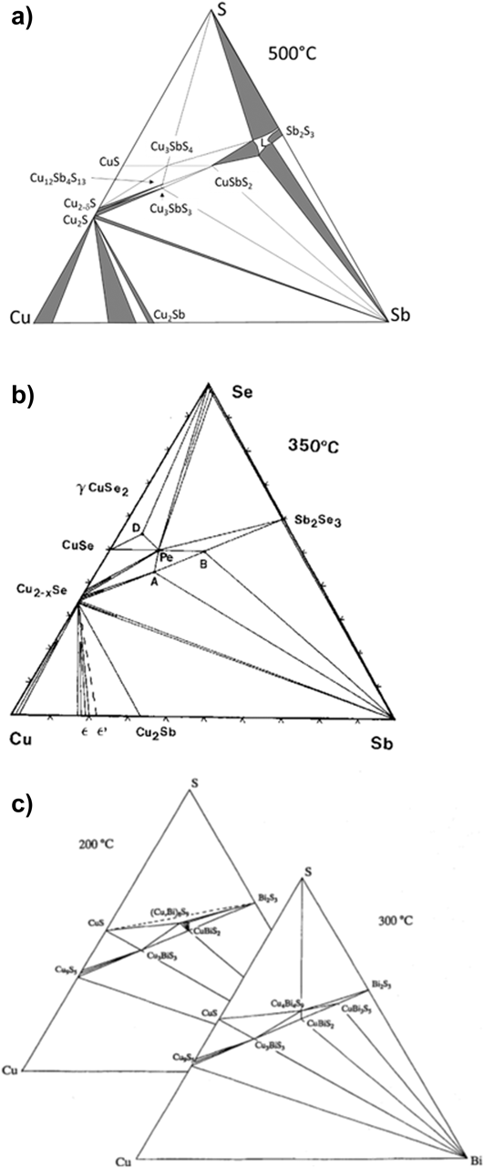
Each of the ternary groups Cu–Sb–S, Cu–Sb–Se, Cu–Sb–Te, Cu–Bi–S, Cu–Bi–Se, and Cu–Bi–Te, comprise a wide range of compounds which are listed in Table 1 but are more easily visualized from triangular phase diagrams—a selection is shown in Fig. 1. Much of the early work on this class of materials was driven by ore mineralogy which distinguishes ternary metal sulfides as ‘sulfo-salts’, a subclass of the chalcogenides. The interested reader is referred to MoeloReference Moelo, Makovicky, Mozgova, Jambor, Cook, Pring, Paar, Nickel, Graeser, Karup-Moller, Balic-Zunic, Mumme, Vurro, Topa, Bindi, Bente and Shimizu7 for a comprehensive account, while a summary of the discoveries of CuSbS2 and Cu3SbS3 for the PV reader are given by Lane et al.Reference Lane, Hutchings, McCracken, Forbes and Irvine8
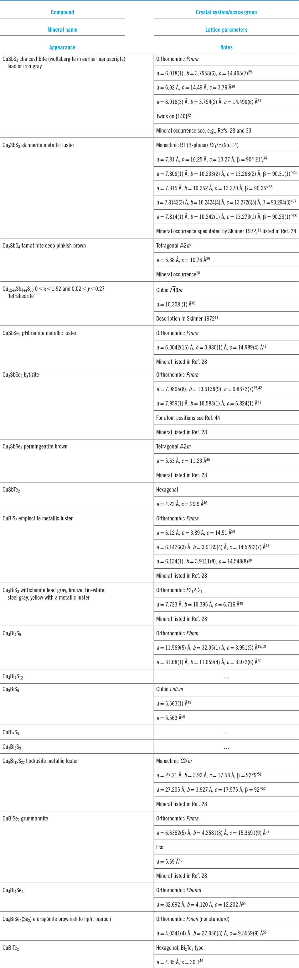
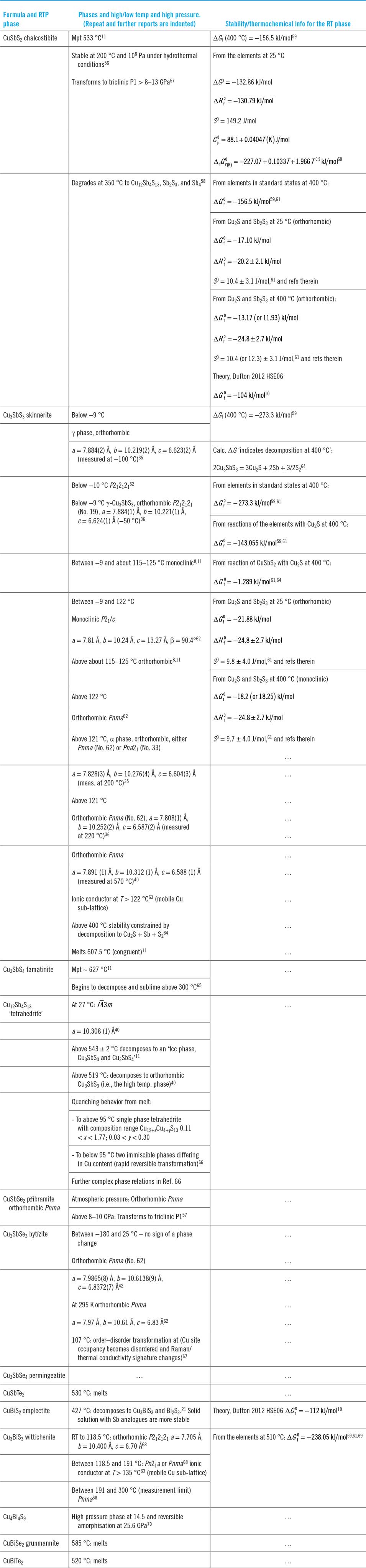
List of Cu–Sb and Cu–Bi chalcogenide phases at room temperature with mineralogical names/appearances and crystallographic data. The crystallographic data are in chronological order. Mineral names are those adopted by International Mineralogical Association only unless in inverted commas. Visual appearances of minerals are from mindat.org.28
Ternary phase diagrams for some Cu–Sb,Bi chalcogenides—the tie lines connect the phases that exist in stable equilibrium. (a) Cu–Sb–S at 500 °C.Reference Skinner, Luce and Makovcky11 (b) Cu–Sb–Se section at 350 °C,Reference Karup-Moller12 and (c) Cu–Bi–S sections at 200 and 300 °C.Reference Wang13 (a) redrawn from Skinner, 1972Reference Skinner, Luce and Makovcky11 and with permission from the Society of Economic Geologists, (b) redrawn from Karup-Moller, 1999Reference Karup-Moller12 www.schweizerbart.de/journals/njma with permission of Schweizerbart Science Publishers, and (c) reproduced with the permission of the Mineralogical Society of Great Britain & Ireland, from Wang, 1994.Reference Wang13
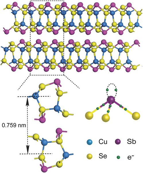
A particular feature of the Sb(III) and Bi(III) compounds is that these ions have Sb5s2 and Bi6s2 lone pairs that block a bonding direction (see Fig. 2). These may be considered as antibonding orbitals that are energetically stabilized by including distortions into the crystal lattice—a detailed appraisal may be found in Ref. Reference Walsh, Payne, Egdell and Watson9. Further work on their influence on the structures of CuSbS2 and CuBiS2 is given by Dufton.Reference Dufton, Walsh, Panchmatia, Peter, Colombara and Islam10 The resulting broken symmetry imparts complex crystal structures to most of the family of compounds, with orthorhombic, monoclinic, and tetragonal unit cells being common (Table 1). These crystal structures often comprise covalently bonded sheets that are themselves connected by van der Waal’s forces along planes of lone pair electron density where covalent bonds may not form. Anisotropy of the physical properties is expected.
The crystal structure of CuSbSe2 showing the layered structure that results from the lone pair on the Sb ion.Reference Xue, Yang, Yuan, Wang, Liu, Zhou, Hu, Pan, Chen and Tang14 Covalently bonded sheets are joined by van der Waals forces. Figure from Xue, 2015,Reference Xue, Yang, Yuan, Wang, Liu, Zhou, Hu, Pan, Chen and Tang14 reproduced with permission from John Wiley.
An important—but yet to be realized—consequence of this structural feature is its potential effect on grain boundaries and their influence on recombination in PV devices. In the better-known diamond-like semiconductors (Si, GaAs, CdTe, CIGS, etc) the bonding is entirely covalent or covalent/ionic. The wrong- or dangling-bonds at grain boundaries are generally considered to be associated with electronic energy levels that are deep in their band gaps, and hence able to promote rapid Shockley–Hall–Reed recombination. This harms both the open circuit voltage (V oc) and short circuit currents (J sc) of PV devices. However, it has been pointed out that for compounds with mixed covalent and van der Waals bonding (e.g., the ribbon-bonded compound Sb2Se3Reference Zhou, Wang, Chen, Qin, Liu, Chen, Xue, Luo, Cao, Cheng, Sargent and Tang15), it is in principle possible for the grain boundaries in crystallographically textured films to be van der Waal’s bonded, and hence to contain no bad covalent bonds. Engineered formation of low recombination boundaries by means of encouraging aligned needle-like grains through the use of the ‘structure zone model’Reference Messier, Giri and Roy16 has yet be demonstrated in practice for any material, let alone the Cu–Sb,Bi-chalcogenides.
A second consequence of the mixed bonding in the Sb(III) and Bi(III) is that the phonon dispersion relations are affected and hence they have low thermal conductivity. For example, Ref. Reference Du, Zhang, Chen, Mahajan and Reece17 used calculations to compare CuSbS2 and its Fe analogue—the lone pairs present in the Sb, but not the Fe compound were responsible for extra phonon scattering and hence low thermal conductivity. This combination of low thermal with high electrical conductivity has led to some interest from the thermoelectric community but without any remarkable demonstrations of any high ZT figure of merit to date (see “Other applications”).
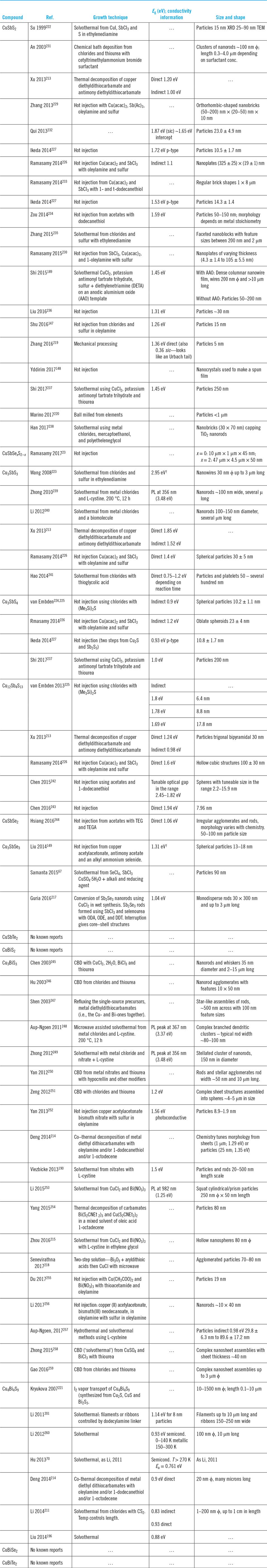
While there are many members of this family of compounds, the most commonly reported ones are analogous to CuSbS2, Cu3SbS3, Cu3SbS4, and Cu12Sb4S13, i.e., substituted with Bi, Se, and Te. In addition, the Cu–Bi–S series contains the phase Cu4Bi4S9 which is a recognized mineralogical phase that has been studied for its crystal structure.Reference Takeuchi and Ozawa18–Reference Bente and Kupcik20 Of these, the most important compounds for PV to date are CuSbS2 (>90 papers) and Cu3BiS3 (>60 papers, but no devices), although there are some remarkable but as yet unverified claims for Cu4Bi4S9 (see “Photovoltaic devices—predictions of performance, design of devices and technological status” and Table 10).
Of the many unusual stoichiometries, ‘tetrahedrite’ requires special explanation. Named for its striking crystal habit in natural deposits, the Sulfosalt Sub-committee of the International Mineralogical Association Commission on Ore MineralogyReference Moelo, Makovicky, Mozgova, Jambor, Cook, Pring, Paar, Nickel, Graeser, Karup-Moller, Balic-Zunic, Mumme, Vurro, Topa, Bindi, Bente and Shimizu7 lists tetrahedrite as Cu6[Cu4(Fe,Zn)2]Sb4S13, i.e., with the sum of Cu and Fe and/or Zn being 12. Indeed, the name ‘tetrahedrite’ is used in the literature to embrace a multiplicity of substituted compositions. Its pure ternary analogue, and the only one relevant here, is Cu12Sb4S13. Deviations from this stoichiometry (the existence region of ‘tetrahedrite’ in phase space) were identified as Cu12+xSb4+yS13 0 ≤ x ≤ 1.92 and 0.02 ≤ y ≤ 0.27 by Skinner.Reference Skinner, Luce and Makovcky11 The bismuth substituted analogues are named bismuthian tetrahedrites.
Given that Sb may substitute for Bi, and the chalcogens are all interchangeable, it is to be expected that many of the Cu–Sb,Bi chalcogenides will form solid solutions with their analogues. The few that have been studied are as follows:
(i) CuSbS2–CuBiS2: Existence of a continuous solid solution across whole composition range was verified by synthesis from the elements in the tube reaction at 310 °C (although success of forming the Bi-rich compounds depends on the heating schedule used, see Ref. Reference Razmara, Henderson, Pattrick, Bell and Charnock21). CuBiS2 is thermally unstable to decomposition to Cu3BiS3 and Bi2S3 at 427 °C, but addition of Sb increases stability, and for x ≥ 0.3, decomposition is not observed.Reference Razmara, Henderson, Pattrick, Bell and Charnock21 An unrelated paper on analytical methods demonstrated that the accuracy of ‘abrasive stripping voltammetry’ is x ± 0.03 for the same solid solution.Reference Meyer, Zhang and Scholz22
(ii) CuSbS2–CuSbSe2: The full composition range of ‘mesocrystals’ was synthesized by the hot injection method and shows almost linear Vegard’s plots for a, b, and c. Reference Ramasamy, Gupta, Palchoudhury, Ivanov and Gupta23 Theory also supports the linear variation of the band gap with composition.Reference Takei, Maeda and Wada24,Reference Wada, Maeda, Maiberg, Franzel and Scheer25
(iii) Cu3SbS3–Cu3BiS3: MaielloReference Maiello, Zoppi, Miles, Pearsall and Forbes26 fabricated the full composition range and demonstrated linear behavior of Vegard’s law for band gap.
(iv) Cu12Sb4S13–Cu12Bi4S13: KumarReference Kumar, Chetty, Femi, Chattopadhyay, Malar and Mallik27 made the full composition range by direct reaction of the elements.
Table 2 shows the high and low temperature phases of the Cu–Sb,Bi chalcogenides and also the Gibbs free energies of formation of the room temperature phases.
Phase transformations and thermochemical information. (Second, and further confirmatory reports of data in columns 2 and 3 are indented).
Phase changes in the range of PV device operation
Since the normal temperature range of operation for solar PVs is from an upper limit of about 60 °C down to the winter minimum, few compounds in the series have phase transitions that would compromise the stability of PV devices in service. However, Cu3SbS3 would be susceptible to low temperatures, undergoing a transition from monoclinic to orthorhombic at −9 °C, which probably rules it out for PV applications in some climates. Its bismuth analogue, Cu3BiS3 has a phase transition at 118.5 °C, but this is above the likely operating range for PV.
Thermal decomposition
Thermal decomposition information is available for a limited range of the compounds. The onset of degradation has been recorded as follows (see Table 2): CuSbS2 > 400 °CReference Welch, Zawadzki, Lany, Wolden and Zakutayev58; Cu3SbS3 > 400 °CReference Seal, Essene and Kelly64; Cu3SbS4 > 300 °CReference Franzer, Paudel, Xiao and Yan65; Cu12Sb4S13 519 °CReference Lemoine, Bourges, Barbier, Nassif, Cordier and Guilmeau40 or 543 ± 2 °CReference Skinner, Luce and Makovcky11; and CuBiS2 472 °C.Reference Razmara, Henderson, Pattrick, Bell and Charnock21 These relatively low temperatures, especially for the former three, may cause problems for the formation of films using methods where the substrate temperature is expected to exceed the decomposition point, e.g., close space sublimation.
Ternary phase diagrams, pseudo-binary phase diagrams, and reactions
Cu–Sb–S system
The ternary isothermal phase diagrams (see Fig. 1) indicate the stable phases and their relationships at a given temperature. For the Cu–Sb–S system, the earliest determinations were by SkinnerReference Skinner, Luce and Makovcky11 who made an experimental evaluation of the behavior of the main phases in the range 400–600 °C, including, for example, evaluation of the temperature dependence of the existence region of ‘tetrahedrite’ Cu12SbS13. Follow-on work by BragaReference Braga, Ferreira, Lopes, Malheiros, Marques, Silva, Baptista, Sa, Alves, Malheiros and Vieira71 largely confirmed Skinner’s findings and there is a comprehensive summary by Tesfeye Firdu.Reference Tesfeye Firdu61
As may be expected, some of the principal phases in the Cu–Sb–S plane lie on lines connecting significant binary phases. For example, both CuSbS2 and Cu3SbS3 lie directly on the Cu2S–Sb2S3 line. Hence the pseudo-binary phase diagrams are of interest in informing the stability, reactions, and synthesis of the main phases. Figure 3 shows the Cu2S–Sb2S3 pseudo-binary diagramReference Tesfeye Firdu61,Reference Cambi and Elli72 and this highlights the possibility of reactions of Cu2S and Sb2S3 to form either CuSbS2 or Cu3SbS3. Indeed, the combination of binary compounds has been used to inform the bulk and thin film synthesis of this class of ternary materials more generally, either from solid state reactions or by co-sputtering, for example, as described in the section “Formation and properties of bulk, thin film and nanoparticle materials”.
Pseudo-binary phase diagram of Cu2S–Sb2S3. Adapted from Cambi, 1965,Reference Cambi and Elli72 and also appears in Tesfeye Firdu, 2010.Reference Tesfeye Firdu61 A simplified version also appears in Ref. Reference Taras Bryndzia and Kleppa75.
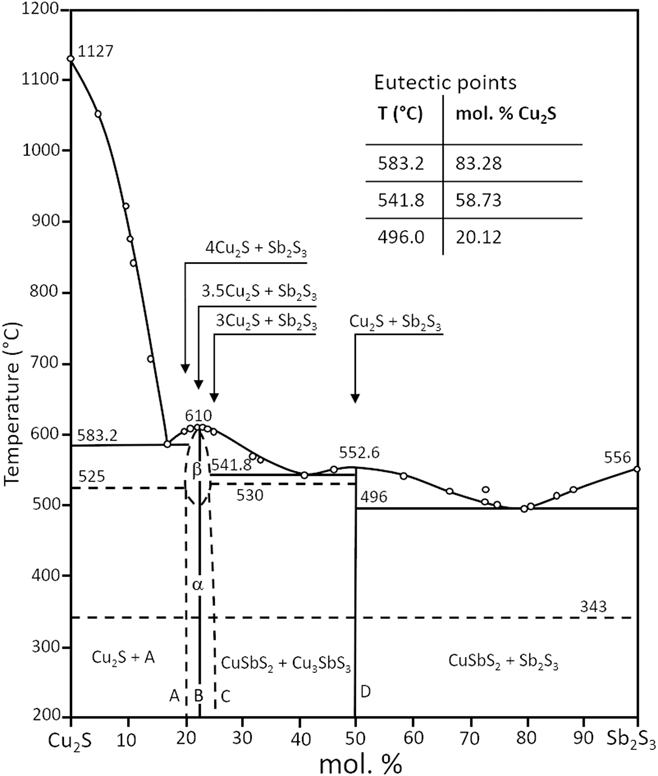
For a full description of the phase diagrams, phase relations, and reactions in the Cu–Sb–S system, the reader is referred to the comprehensive review by Tesfeye Firdu.Reference Tesfeye Firdu61 The reader is reminded that the Cu–S phase diagram and that the number and type of phases of the Cu2−δS compounds is itself very complex—the binary phase diagram and the main phases are reported in Ref. Reference Chakrabarti and Laughlin73.
Cu–Sb–Se and Cu–Sb–Te systems
The ternary diagram is shown in Fig. 1 for 350 °CReference Karup-Moller12 and has considerable similarities with that of Cu–Sb–S. Karup-Moller’s paperReference Karup-Moller12 is comprehensive, giving the three binary Se–Cu–Sb–Se phase diagrams plus a thorough determination of the Cu–Sb–Se triangle at 300, 400, 450, 500, 600, and 700 °C.
No triangular phase diagram is known to the author for Cu–Sb–Te.
Cu–Bi–S system
Ternary isotherms for Cu–Bi–S were determined by Wang et al.Reference Wang13 at 200 and 300 °C, while the pseudobinary Cu2S–Bi2S3 T–x phase diagram is reported by Chang.Reference Chang, Neumann and Choudary69 Both are contained in Tesfeye Firdu’s reviewReference Tesfeye Firdu61 along with accounts of the main reactions and the Gibbs free energies of formation of Cu9BiS6, Cu3BiS3, Cu3Bi5S9, and CuBi3S5—from the elements, and from the elements in various combinations with either Cu2S or one of several other Cu–Bi–S compounds.Reference Craig and Lees59,Reference Chang, Neumann and Choudary69 The thermochemical data come from solid state galvanic cell e.m.f measurements.Reference Schmidt, Sagua and Lescano74
A significant difference between the Cu–Bi–S and Cu–Sb–S systems is the presence of the Cu4Bi4S9 phase, for which the Sb analogue is not recorded. Cu4Bi4S9 is a well-documented uncontroversial orthorhombic phase that has been the subject of several crystallographic investigations.Reference Takeuchi and Ozawa18–Reference Bente and Kupcik20
Cu–Bi–Se and Cu–Bi–Te systems
No phase diagrams have been reported to date to the author’s knowledge.
Interaction of copper antimony sulfides with CIGS and ZnS
A further aspect of the copper antimony chalcogenides is that Sb has been reported to promote the formation and subsequent metallurgical change in Cu(In,Ga)Se2 (CIGS). The key intermediate is Cu3SbSe3.
Sintering aid for chalcopyrites and kesterites
The lower melting point of CuSbS2 compared to CuInSe2 enables it to act as a sintering aid for thermal processing of CuInSe2 solar cell materials. The use of SbCl3 in this context is explained in Ref. Reference Yang, Wang, Li, Wan and Huang76. Korzun gives the relevant pseudobinary phase diagram.Reference Korzun, Gavrilenko, Fadzeyeva, Ignatenko, Maroz, Sobol, Rusu, Klenk, Merschjann, Schedel-Niedrig and Lux-Steiner77 Xiang, in work on Cu(In,Ga)Se2 (CIGS), identifies Cu3SbSe3 as an important intermediate.Reference Xiang, Zhang and Zhang78
It is used similarly with Cu2ZnSnS4 (CZTS)Reference Guo, Cui, Tian, Gao, Wang and Pan79 in which it promotes grain growth, although Sb2S3 is more effective.
The mineralogical literatureReference Seal, Essene and Kelly64 evaluated the interaction of Cu3SbS3 with ZnS and identified the reaction:
 $${\rm{4C}}{{\rm{u}}_3}{\rm{Sb}}{{\rm{S}}_3} + 2{\rm{ZnS}} = {\rm{C}}{{\rm{u}}_{10}}{\rm{Z}}{{\rm{n}}_2}{\rm{S}}{{\rm{b}}_4}{{\rm{S}}_{13}} + {\rm{C}}{{\rm{u}}_2}{\rm{S}}\quad {\rm{,}}$$
that is, ZnS is a thermodynamically unsuitable partner layer for Cu3SbS3 in PV devices.
Formation and properties of bulk, thin film and nanoparticle materials
This section reviews the methods used to form the compounds in their bulk, thin film and nanoparticle forms. Since these materials comprise the basis of the experimental reports of band gap, conductivity and optical dispersion, this section also provides a comprehensive account, including the results of theoretical calculations.
Bulk synthesis methods (see Table 3)
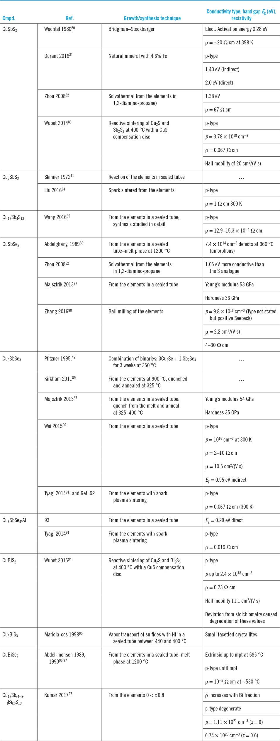
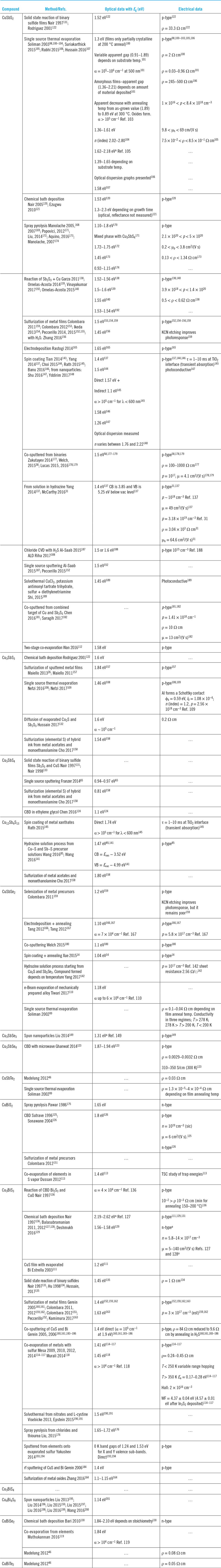
A full palate of methods has been used to form the bulk materials, there being a total of just over 20 reports in all. While there are isolated studies of the optical and electrical properties of naturally occurring minerals, e.g., CuSbS2,Reference Durant and Parkinson81 the presence of impurities (nearly 5% Fe in this case) makes artificial synthesis preferable for reliable physical studies. A summary of the laboratory methods used follows, while Table 3 provides a comprehensive review of the literature reports of bulk synthesis including the band gaps and conductivity properties of the products.
Formation of the bulk compounds and associated reports of their conductivity type, band gap, and resistivity where available.
Bulk synthesis from the elements (in tubes; by spark; ball milling and solvothermal methods)
Direct combination of the elements is favourable energetically and several methods have been used to achieve it in practice.
Synthesis from the elements in sealed tubes is the most widely reported method and has been demonstrated for Cu3SbS3,Reference Wubet and Kuo83 ‘tetrahedrite’ Cu12Sb4S13 and its mixed Sb–Bi analogue,Reference Wang, Gu, Bao, Li and Chen85 CuSbSe2,Reference Abdelghany, Abdelmohsen, Abouelela and Abdelwahab86,Reference Majsztrik, Kirkham, Garcia-Negron, Lara-Curzio, Skoug and Morelli87 Cu3SbSe3,Reference Majsztrik, Kirkham, Garcia-Negron, Lara-Curzio, Skoug and Morelli87,Reference Kirkham, Majsztrik, Skoug, Morelli, Wang, Porter, Payzant and Lara-Curzio89,Reference Wei, Wu, Sun, Pan and Li90 and CuBiSe2.Reference Abdelmohsen, Abdelghany and Sharaf96,Reference Abdelmohsen, Abdelghany, Abouelela and Abdelwahab97 Spark sintering of the elements has been used for Cu3SbSe3Reference Liu, Ren, Tan, Lin and Nan84 and Cu3SbSe3Reference Tyagi, Gahtori, Bathula, Toutam, Sharma, Singh and Dhar91; and.Reference Tyagi, Gahtori, Bathula, Toutam, Sharma, Singh and Dhar91,Reference Tyagi, Gahtori, Bathula, Srivastava, Shukla, Auluck and Dhar92 The elements may also be combined by ball milling at room temperature to produce powder. While for the present family of compounds, this has only been demonstrated for CuSbSe2,Reference Zhang, Yang, Jiang, Fu, Xiao, Luo and Zhou88 the method has been used for CdTe and CZTS and may be expected to be general. The elements have been combined by solvothermal synthesis in 1,2-diamino-propane to form CuSbS2 and CuSbSe2,Reference Zhou, Bian, Zhu, Zhang, Li and Dai82 although to date this has only been the subject of a single paper as a method of making bulk materials.
Bulk synthesis from the binary compounds
Reactions highlighted from the pseudo-binary phase diagrams have been exploited to form CuSbS2, Cu3SbSe3, and CuBiS2: For CuSbS2, CuS, and Sb2S3 were heated in the presence of a compensation disk to prevent volatile escape.Reference Wubet and Kuo83 For Cu3SbSe3, the binaries were combined in the ratio 3Cu2Se + 1Sb2Se3 and then heated for 3 weeks at 350 °C in a quartz capsule.Reference Pfitzner42 For CuBiS2, Cu2S was combined with Bi2S3 at 400 °C, again with a CuS compensator.
MajsztrikReference Majsztrik, Kirkham, Garcia-Negron, Lara-Curzio, Skoug and Morelli87 considers that the formation of Cu3SbSe3 from the elements proceeds via the intermediates Cu2S and CuSbSe3 and that the rate of the reaction is controlled by their solid state interdiffusion. Possibly this is general, but it has not been investigated for other compounds.
Crystal growth
There are few reports. WachtelReference Wachtel and Noreika80 grew CuSbS2 by the Bridgman–Stockbarger method; Mariolacos grew Cu3BiS3 octahedral crystallites by HI vapor transport and gives a thorough thermochemical evaluation of the options for process chemistries.Reference Mariolacos95
Thin film formation methods
This section outlines the methods of formation as applied to the whole series of compounds and listed by the method.
Single source evaporation
Evaporation (physical vapor deposition) is quite widely used but given the propensity for the compounds to lose components, many of the reports contain accounts of post-growth annealing in the chalcogen to correct for losses.
For CuSbS2, see Refs. Reference Soliman, Zayed, El Soad and El Ghafar98–Reference Hussain, Ahmed, Ali, Butt, Shaari, Shamsuri, Khenata, Prakash and Verma107; For Cu3SbS3, Refs. Reference Nefzi, Rabhi and Kanzari108 and Reference Nefzi, Rabhi and Kanzari109; for CuSbSe2, see Ref. Reference Soliman, Aziza, El-Soad, Zayed and El-Ghfar99 and by e-beam, see Ref. Reference Tiwari, Vinod, Subrahmanyam and Malar110; for CuSbTe2, see Ref. Reference Soliman, Aziza, El-Soad, Zayed and El-Ghfar99; for Cu3BiS3, see Ref. Reference Estrella, Nair and Nair111.
Co-evaporation
Co-evaporation affords greater stoichiometric control, preventing the loss of individual components, notably the chalcogen. For example, S is sometimes provided from an effusion source, but there are variants with multistep evaporation sequences.
For CuSbS2 (multistep), see Ref. Reference Wan, Ma, Hu, Zhou, Mao, Pan, Wong and Xu112 and for CuBiS2, see Ref. Reference Dussan, Murillo and Mesa113; for Cu3BiS3—see a number of similar reports from Mesa et al.,Reference Mesa, Dussan and Gordillo114–Reference Mesa and Fajardo117 also Ref. Reference Murali, Madhuri and Krupanidhi118; for CuBiSe2, see Ref. Reference Muthukannan, Prema, Henry, Mohanraj and Sivakumar119.
Chemical bath deposition
Most commonly, chemical bath deposition (CBD) is conducted by decomposing thiourea in the presence of the aqueous metal ions at moderate temperatures. Given the prevalence of CBD for depositing CdS and CZTS, the literature for the sulfo-salts is surprisingly sparse. It has nevertheless been extended to a wide range of them as follows:
For CuSbS2 see Refs. Reference Nair, Rodriguez-Lazcano, Pena, Messina, Campos, Nair, Durstock, Friedman, Gaudiana and Rockett120 and Reference Ezugwu, Ezema and Asogwa121; Cu3SbS3 see Ref. Reference Rodriguez-Lazcano, Nair and Nair122; Cu3SbSe4 see Ref. Reference Ghanwat, Mali, Kharade, Pawar, Patil, Mane, Patil, Hong and Bhosale123 and (in ethylene glycol)Reference Chen, Wang, Zhao, Yang, Chen, Huang, Jian and Ruan124; CuBiS2 see Refs. Reference Sutrave, Shahane, Dargad and Deshmukh125 and Reference Sonawane, Wani, Patil and Seth126; Cu3BiS3 see Refs. Reference Balasubramanian, Suriyanarayanan, Prabahar and Srikanth127–Reference Deshmukh, Panchal, Vipul, Shekhawat, Bhardwaj and Suthar129; CuBiSe2 see Ref. Reference Bari and Patil130.
From combination of binary materials
As mentioned in section “Cu–Sb, Bi–S, Se, Te compounds: crystallographic data, stability and phase diagrams”, the binaries may be expected to react to form the ternaries, for example, NairReference Nair, Nair, Garcia, Pena, Arenas, Garcia and GomezDaza131 combined CBD films to exploit the reaction Sb2S3 + 2CuS → 2CuSbS2 + S(g) in perhaps the earliest report of the formation of a thin film of this material. There is a similar report from Rodriguez-Lazcano.Reference Rodriguez-Lazcano, Nair and Nair122 Subsequent authors combined films deposited by both CBD and other methods. For Cu3SbS3, see Ref. Reference Hussain, Ahmed, Ali, Shaari, Luo and Fu132; for Cu3SbS4, see Refs. Reference Nair, Nair, Garcia, Pena, Arenas, Garcia and GomezDaza131 and Reference Nair, Pena, Campos, Garcia and Nair133; for Cu3BiS3, see Refs. Reference Nair, Nair, Garcia, Pena, Arenas, Garcia and GomezDaza131, Reference Hu, Gomez-Daza and Nair134, and Reference Hussain, Ahmed, Ali, Abdel-Salam, bin Deraman and Fu135. In an unusual variation, NairReference Nair, Huang, Nair, Hu, Meyers and Zingaro136 combined CuO and Bi2S3 to form Cu3SbS3.
There are also solution variants: YangReference Yang, Wang, Han, Zhou, Song, Chen, Zhong, Lv, Niu and Tang137 spun binary precursors from hydrazine to form CuSbS2. McCarthyReference McCarthy, Cottingham, Abuyen, Schueller, Culver and Brutchey31 formed the same material from Cu2S and Sb2S3 in a thiol–amine mixture.
Combination of binaries with Cu films
This has been attempted for CuSbS2 only.Reference Maiello, Zoppi, Miles, Pearsall and Forbes26,Reference Garza, Shaji, Arato, Tijerina, Castillo, Das Roy and Krishnan138–Reference Ornelas-Acosta, Shaji, Avellaneda, Castillo, Das Roy and Krishnan140
From solutions in hydrazine
In addition to CuSbS2 (aboveReference McCarthy, Cottingham, Abuyen, Schueller, Culver and Brutchey31), hydrazine methods have been used for Cu12Sb4S13Reference Wang, Gu, Bao, Li and Chen85,Reference Wang, Yang, Xia, Leng, Zhou, Xue, Zhong, Gao, Song and Tang141 and CuSbSe2.Reference Yang, Wang, Yuan, Chen, He, Song, Ding, Zhao and Tang142 While having the advantage of being a strong reducing agent for use in combination with semiconductor inks, for example, hydrazine is not popular on account of its toxicity and instability. Large area production methods for PV using it are not expected.
Spin coating
Several variations of spin coating have been used, for example, using CBD chemistry or nanoparticles. For CuSbS2, Refs. Reference Yang, Wang, Han, Zhou, Song, Chen, Zhong, Lv, Niu and Tang137 and Reference Tian, Wang, Zhao, Chen, Yang, Huang and Pan143–Reference Banu, Ahn, Ahn, Yoon and Cho146 report wet chemical routes while Refs. Reference Shu and Han147 and Reference Yddirim, Aljabour, Sarilmaz and Ozel148 use nanoparticles in suspension. For Cu12Sb4S13, see Ref. Reference Rath, MacLachlan, Brown and Hague145; for CuSbSe2, see Ref. Reference Xue, Yang, Yuan, Wang, Liu, Zhou, Hu, Pan, Chen and Tang14; for Cu3SbSe3, see Ref. Reference Liu, Yang, Gu, Cao, Su, Jiang, Yan, Hao, Liu and Liu149. Since the hot injection methods can be tailored to form monophase nanoparticles, the spinning route has proved effective for forming specific phases, including Cu4Bi4S9.Reference Liu, Cheng, Wang, Zhang and Gu150 Multiple spin runs were needed to accrete sufficient material to anneal into a film. Generally, spin coating is an excellent lab method but is not suitable for the large scale-up required for PV manufacturing.
Sulfurization of metal films and other starting materials
Following earlier practice with CuInSe2 and CIGS, sulfurization of metal films has been used as a method of controlling the incorporation of volatile components. Use of elemental sulfur is most common. As for bulk vapor transport crystal growth of chalcogenides in sealed tubes, ColombaraReference Colombara151 points out that incorporation of a background pressure of an inert gas in the sulfurization tube can help maintain the composition of the thin film. However, using this method for CuSbS2, it is retention of Sb that is the significant issue.Reference Colombara151 Indeed, Peccerillo conducted trials of the sulfurization of Cu–Sb metal stacks as a function of the Cu/Sb ratio: a 30% excess of Sb was required to achieve 1:1 Cu:Sb stoichiometry for films sulfurized at 400 °C in the particular apparatus used.Reference Peccerillo152
Colombara also compares the use of H2S with that of elemental S: the reduced driving force (free energy of formation) for the former allows for a more controllable reaction, but at the expense of having to handle toxic H2S.Reference Colombara151,Reference Colombara, Peter, Rogers and Hutchings153
Sulfurization of metal ‘precursor’ films has been used to form CuSbS2 with sulfurReference Colombara151–Reference Peccerillo, Major, Phillips, Treharne, Whittles, Dhanak, Halliday and Durose155—with H2SReference Zhang, Li, Li, Li, Zhang, Delaunay and Zhu156; Cu3SbS3Reference Maiello, Zoppi, Miles, Pearsall and Forbes26,Reference Maiello, Zoppi, Miles, Pearsall and Forbes157 —via sulfurization of acetatesReference Cho, Banu, Kim, Park, Yun, Cho and Yoo158; Cu3SbS4—from acetatesReference Cho, Banu, Kim, Park, Yun, Cho and Yoo158; Cu12SbS13—from acetatesReference Cho, Banu, Kim, Park, Yun, Cho and Yoo158; CuSbSe2Reference Colombara, Peter, Rogers, Painter and Roncallo159; CuBiS2,Reference Colombara151 and Cu3BiS3Reference Peccerillo152,Reference Colombara, Peter, Rogers and Hutchings153,Reference Colombara, Peter, Rogers, Painter and Roncallo159–Reference Kamimura, Beppu, Sasaki, Tsubota and Ohno163 —with H2SReference Colombara, Peter, Rogers and Hutchings153,Reference Gerein, Haber, Shafarman, Gessert, Niki and Siebentritt160,Reference Gerein and Haber161 —from sulfurization of oxides.Reference Zhang, Jin, Yuan, Jiang, Liu and Zhu164
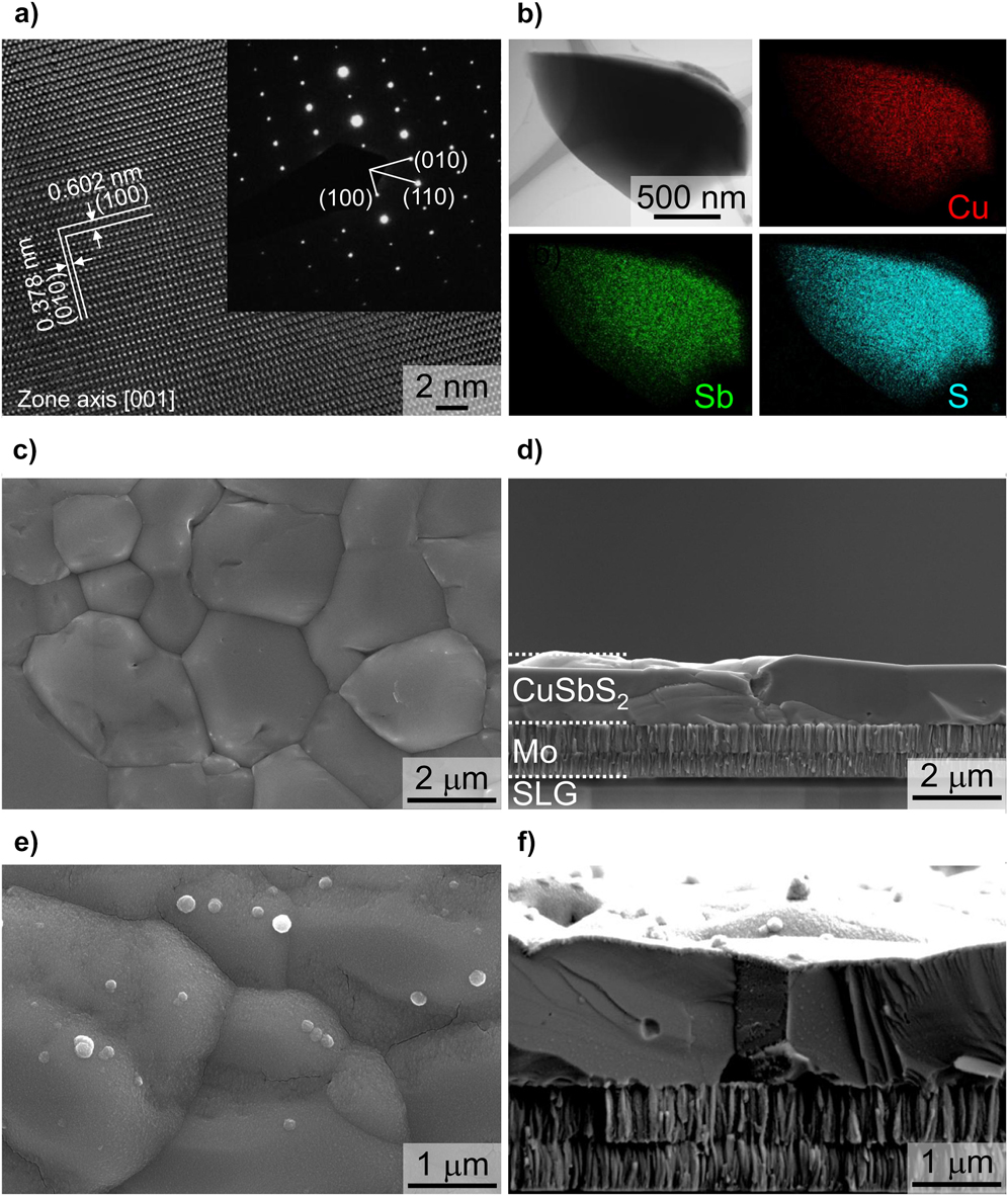
Figure 4 shows microscopy and analysis of a CuSbS2 film grown by H2S sulfurization of electrochemically deposited metal films—the grains are ∼1 μm in size, which is very acceptable for PV applications.
Microscopy of CuSbS2 photocathode structure for hydrogen evolution. The film was formed by sulfurizing electrochemically deposited metal films in H2S. (a) HRTEM of the lattice in [001] projection, (b) elemental mapping of a grain, (c) plan view of a CuSbS2 film, (d) cross section of a ‘substrate’ device structure and (e and f) the same at higher magnification. The CuSbS2 grains are ∼1 μm in size. Figure from Zhang, 2016,Reference Zhang, Li, Li, Li, Zhang, Delaunay and Zhu156 reproduced with permission from Elsevier.
Electrodeposition
Electrodeposition of multernary materials is challenging on account of the differences in deposition potentials between the components. Nevertheless it has been tried for CuSbS2Reference Rastogi and Janardhana165 and CuSbSe2.Reference Tang, Yang, Liu, Lai, Li and Liu166,Reference Tang, Yang, Liu, Lai, Jia, Li and Liu167
Spray pyrolysis
Most usually, this has been tried using CBD-like chemistry, i.e., using a metal salt or acetate and thiourea. The majority of reports have been for CuSbS2,Reference Manolache, Nanu, Duta, Goossens and Schoonman168 2007Reference Manolache, Duta, Isac, Nanu, Goossens and Schoonman169–Reference Manolache and Duta174; For CuBiS2, see Ref. Reference Pawar, Pawar and Bhosale175 and for Cu3BiS3, see Ref. Reference Liu, Wang, Nie, Chen and Yuan176.
Sputtering
Co-sputtering of the binaries is most effective and is analogous to the method of combining binary films to form the ternary. There are relatively few reports—for CuSbS2, see Refs. Reference Welch, Zawadzki, Lany, Wolden and Zakutayev58, and Reference Zakutayev, Baranowski, Welch, Wolden and Toberer177–Reference Lucas, Welch, Baranowski, Dippo, Hempel, Unold, Eichberger, Blank, Rau, Mascaro and Zakutayev179; for CuSbSe2, see Ref. Reference Welch, Baranowski, Zawadzki, Lany, Wolden and Zakutayev180.
Co-sputtering of Sb2S3 with Cu has been used to form CuSbS2.Reference Chen, Kuo and Tuan181,Reference Saragih, Kuo and Tuan182 Gerein makes a number of self-similar reports of the formation of Cu3BiS3 by co-sputtering CuS with Bi.Reference Gerein, Haber, Shafarman, Gessert, Niki and Siebentritt160,Reference Gerein and Haber161,Reference Gerein and Haber183–Reference Gerein and Haber186
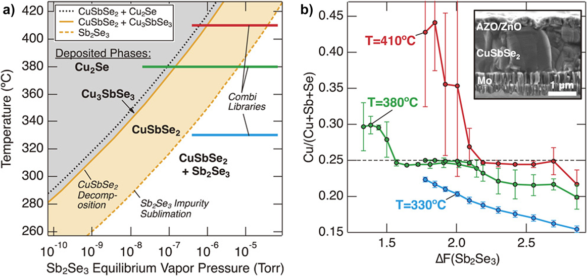
WelchReference Welch, Baranowski, Zawadzki, Lany, Wolden and Zakutayev180 gives a particularly insightful study of the preparation of CuSbSe2 by co-sputtering Cu2Se and Sb2Se3: First, they recognized that the phases present in the film would be limited by both temperature and the supply of Sb2Se3. At high temperatures, CuSbSe2 is expected to decompose, although this can be suppressed by supplying Sb2Se3. However, excessive pressures of Sb2Se3 would encourage the formation of a CuSbSe2 + Sb2Se2 mixture. Figure 5(a) shows a calculated map of the expected phases on the T–p(Sb2Se3) plane and the band for which mono-phase CuSbSe2 is expected. To explore a wide range of preparation conditions in a single run, they used nonrotating substrates to generate combinatorial samples, and their composition ranges are shown as lines in Fig. 5(a). The experimental outcome appeared to validate the phase map, with the film composition being controlled by the (spatially varying) local ratio of the supply of Sb2Se3 to Cu2Se [Fig. 5(b)]. The resulting films had an optical band gap of 1.1 eV, an absorption coefficient of about 105 cm−1, hole concentrations of 1017 cm−3, and micron-sized grains.
Preparation of CuSbSe2 by co-sputtering Sb2Se3 and Cu2Se on a nonrotating substrate to generate combinatorial (multicomposition) films. (a) Calculated phase map on the T–p(Sb2Se3) plane. High temperatures are expected to cause decomposition while high pressures of Sb2Se3 may cause co-deposition of CuSbSe2 and Sb2Se3. There is a central target band of growth conditions. Varying the spatially dependent flux of Sb2Se3 during combinatorial deposition allowed the three colored lines in (a) to be explored, and compositional analysis of them is shown in (b) as a function of the effective ratio of Sb2Se3/Cu2Se (labeled ΔF). The flat regions correspond to the formation of monophase CuSbSe2. Figures reproduced from Ref. Reference Welch, Baranowski, Zawadzki, Lany, Wolden and Zakutayev180 with permission from the Japan Society of Applied Physics. Copyright 2017 The Japan Society of Applied Physics.
Single target sputtering of ternaries is generally thought to be problematic, with the target composition drifting with sputtering time. The limited attempts to make it work for CuSbS2 are reported in Refs. Reference Peccerillo152 and Reference Al-Saab187 and for Cu3SbS3,Reference Franzer, Paudel, Xiao and Yan65 it is not recommended.
CVD and ALD
CuSbS2 has been made by CVDReference Al-Saab187 from the chlorides and H2S. ALDReference Riha, Koegel, Emery, Pellin and Martinson188 was conducted with H2S, bis(N,N′-disecbutylacetamidinato)dicopper(I) (CuAMD) and tris(dimethylamido)antimony(III) but required ∼2500 cycles to produce usable films: it is unlikely to become popular.
Solvothermal growth
This is reported for CuSbS2 (CuCl2–2H2O, potassium antimonyl tartratetrihydrate, elemental sulfur, and diethylenetriamine)Reference Shi, Li, Wu and Dai189 and Cu3BiS3 (from nitrates and L-cystine).Reference Viezbicke and Birnie190,Reference Epstein, Castellano, Shan and Birnie191 This method is more often used for nanoparticles.
Deep levels and traps
Deep levels in the fundamental gap of a semiconductor are of critical importance for the operation of solar cells since the recombination that they enable is deleterious to the voltage achievable from PV devices. Solar cells are minority carrier devices, and V oc is strongly correlated with the minority carrier lifetime.
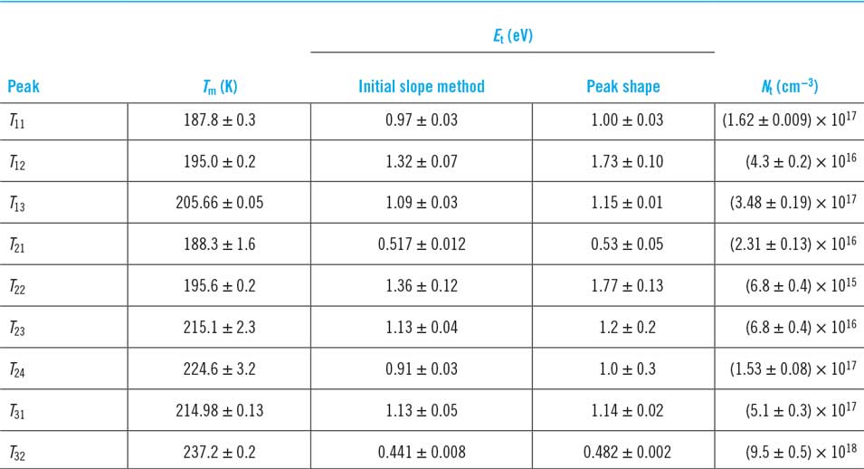
The only experimental study of deep levels reported for any of this family of materials is that by DussanReference Dussan, Murillo and Mesa113 for Cu3BiS3 using the thermally stimulated current method. The data are shown in Table 5. Nine individual traps were determined, and they have high concentrations in the material. Harm to PV performance from the traps in this particular sample is expected.
There is an important opportunity for deep level investigations to be performed on other materials in the series, particularly those that have been used in lab-scale solar cells—the efficiencies to date are not high but the underlying causes have not been identified. It must be a concern for multernary and potentially multiphase materials that deep levels are an issue, particularly in the light of the results in Table 5 for Cu3BiS3.
Band gaps and optical absorption/optical dispersion
All experimental reports indicate that optical absorption is high for the whole series of materials (Table 4) and that many of them have band gaps within the optimum range of 1.1–1.6 eV required for efficient PV absorber operation. Moreover, the majority are p-type, making them compatible with the industry standard n-type transparent electrodes and n-type window layers.
Growth, band gaps, and conductivity types of films.
CBD = chemical bath deposition.
WF = work function.
CB/VB = conduction/valence bands.
a Possibly unreliable.
Trap energies in Cu3BiS3 as determined from thermally stimulated current measurements.Reference Dussan, Murillo and Mesa113 The temperatures T m are the signal peaks, while the trap energies E t were evaluated from the data by two methods and with some consistency. N t is the trap density.
Nevertheless, ab initio calculations (Table 6), where they have been done, indicate that the lowest gaps for the whole series of compounds are for indirect transitions. However, direct transitions exist for energies just a fraction of an electron volt higher.
Ab initio theory studies of the band properties of the Cu–Sb and Cu–Bi chalcogenides. Most studies of most of the compounds concur that the lowest fundamental transition is indirect and that the lowest direct transition is a fraction of an eV higher. Nevertheless, both theory and experiment show them to be exceptionally strong absorbers and hence possible candidates for PV devices: There is no indication at present that their band properties will be disadvantageous.
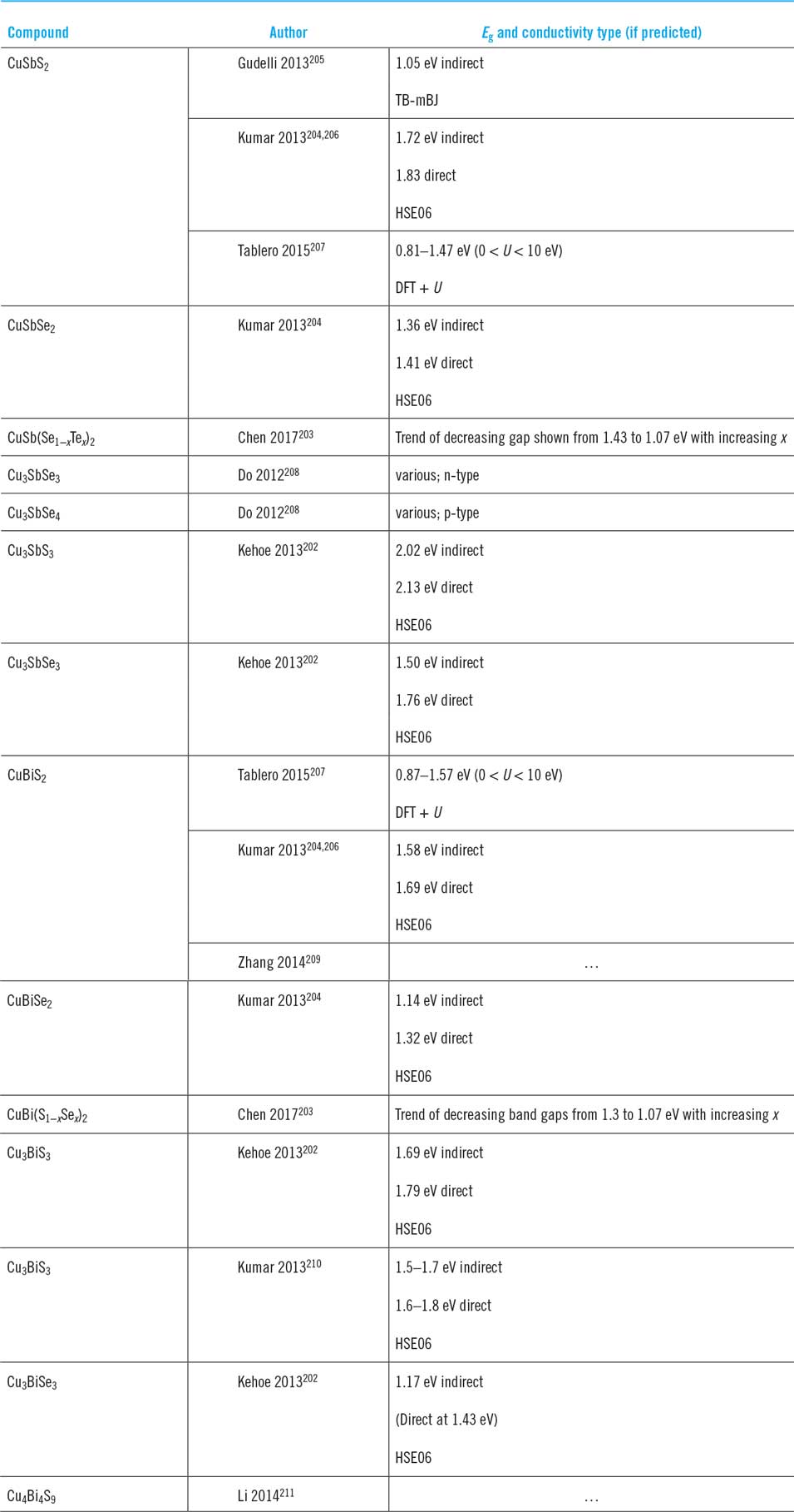
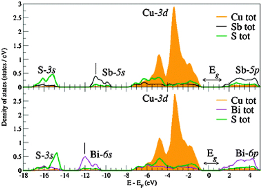
Examples include Dufton for CuSbS2 and CuBiS2 (Fig. 6, showing the valence band being dominated by Cu d10 states)Reference Dufton, Walsh, Panchmatia, Peter, Colombara and Islam10 and Kehoe for Cu3SbS3 and Cu3SbSe3.Reference Kehoe, Temple, Watson and Scanlon202 The solid solutions behave similarly: Takei and Wada report CuSb(S,Se)2Reference Takei, Maeda and Wada24,Reference Wada, Maeda, Maiberg, Franzel and Scheer25 and Chen reports both CuSb(Se,Te)2 and CuBi(S,Se)2.Reference Chen and Persson203 An experimental determination for the solid solution series Cu3Sb(S,Se)3 demonstrated a linear Vegard’s plot for band gap,Reference Maiello, Zoppi, Miles, Pearsall and Forbes26 but did not identify the two kinds of transition. Indeed, clear identification of direct and indirect transitions is difficult using in practice using the routine Tauc methods most commonly reported in the literature. An exception is for Cu3BiS3 for which the zero Kelvin band gaps of 1.24 and 1.53 eV were measured photoreflectance methods for the ‘X’ and ‘Y’ valence sub-bands.Reference Yakushev, Maiello, Raadik, Shaw, Edwards, Krustok, Mudryi, Forbes and Martin193,Reference Yakushev, Maiello, Raadik, Shaw, Edwards, Krustok, Mudryi, Forbes, Martin, Gordon, Valenta, Turan, Atwater and Mirabella194
Density function theory calculations of the band character in CuSbS2 (top) and CuBiS2 (bottom). The tops of the valance bands are dominated by Cu+ d10 filled states, similar to CZTS and CIGS. Figure from Dufton, 2012.Reference Dufton, Walsh, Panchmatia, Peter, Colombara and Islam10 Reproduced by permission of the PCCP Owner Societies.
Xue reports the temperature dependence of the band gap of CuSbSe2Reference Xue, Yang, Yuan, Wang, Liu, Zhou, Hu, Pan, Chen and Tang14 and finds it to conform to a Varshni-type functionReference Xue, Yang, Yuan, Wang, Liu, Zhou, Hu, Pan, Chen and Tang14:
 $${E_{\rm{g}}}\left( T \right) = 1.176 - {{5.486 \times {{10}^{ - 4}}{T^2}} \over {T + 24.673}}\;\left( {{\rm{eV}}} \right)\quad .$$
Despite this family of compounds having lowest indirect rather than direct gaps, practically speaking optical absorption is strong for them all, with absorption coefficients in the range 104–105 cm−1 being common. The number of similar reports suggests that this high level of absorption is genuine (even though it is becoming increasingly expected to have to report the absorption coefficients in the introductions of papers on new PV materials as being >105 cm−1, whether it has been measured or not!). Moreover, calculated absorption spectra support the finding that the absorption coefficients of CuSbS2, CuBiS2, and similar compounds exceed those of the better-known absorbers CuInS2 and CuInSe2, for example, as shown in Fig. 7.Reference Kumar and Persson204
Calculated absorption spectra for CuBiS2 and CuBiSe2 in comparison to CuInS2 and CuInSe2. The Cu–Bi chalcogenides show stronger absorption than the Cu–In ones. Calculations also show similarly strong absorption for CuSbS2 and CuSbSe2. From DFT HSE06 calculations—figure from Kumar, 2014Reference Kumar and Persson204 reproduced with permission from Elsevier.

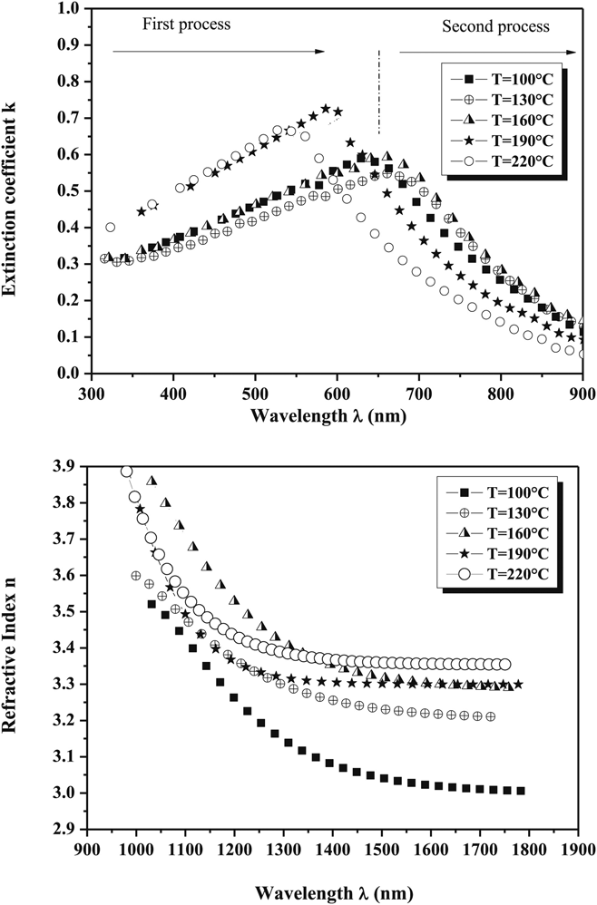
Full knowledge of the optical dispersion relations for the thin film components of PV devices is essential for the prediction and modeling of the optical performance solar cells. Full dispersion data for CuSbS2 thin films are reported for a range of preparation conditions as shown in Fig. 8.Reference Rabhi, Fadhli and Kanzari106 The data for these thin films differ slightly from that of Yddrim for nanoparticlesReference Yddirim, Aljabour, Sarilmaz and Ozel148 due to scattering. Apart from this, for CuSbS2, there are occasional single wavelength measurements, as shown in Table 4. None of the other compounds in the series appear to have had their dispersion relations measured. This is a significant omission from the literature.
Optical dispersion relations for CuSbS2 films fabricated by evaporation from bulk ingots and presented as a function of the post-growth annealing temperature.Reference Rabhi, Fadhli and Kanzari106 Despite their value in modeling solar cell performance, there are very few reports of dispersion relation measurements for the whole family of compounds. Figure from Rabhi, 2015,Reference Rabhi, Fadhli and Kanzari106 reproduced with permission from Elsevier.
Summary of optical band gap values
Tables 4 and 6 give comprehensive lists of the experimental and theoretical band gap values reported for this class of materials while the section ‘Band gaps and optical absorption/optical dispersion’ has discussed the physics of the transitions. Table 7 provides a summary of the experimental values where they are available. Since there are many reports for some of the compounds (e.g. CuSbS2), average values of the reported optical gaps listed in Table 4 have been shown here. In cases where the original work uses the Tauc plot method, and the resulting graph does not have a convincing straight line section for extrapolation, then that data has been excluded from the average. However, for Cu3SbSe3 there is a single report for which the data does not look reliable, but it has been included for completion. Bandgap measurements for CuSbTe2, Cu3BiS4, Cu3BiSe3, Cu3BiSe4, and CuBiTe2 have not been reported in the literature to date.
Band gaps of the Cu–Sb and Cu–Bi chalcogenides. These are average values of the experimental optical band gaps taken from Table 4. Where the band gaps in the source papers have been from nonlinear sections of Tauc plots, the data were excluded, except for Cu3SbSe3 for which there is only one report. For CuBiSe2, there is a single paper which reports the range of values given in the table.
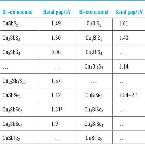
a Possibly unreliable data.
Conductivity type (electronic) and point defect energetics
The majority of the compounds in this family are naturally p-type. For example, there are just over 30 independent reports of hole conduction in CuSbS2. Similarly, Cu3BiS3 is widely reported to be p-type and the isolated report from one author of its being n-type is probably in error. CuBiS2 is less clear: there are two reports of n-type filmsReference Sonawane, Wani, Patil and Seth126,Reference Pawar, Pawar and Bhosale175 and two reports of p-type material, in thin filmReference Sutrave, Shahane, Dargad and Deshmukh125 and bulkReference Wubet, Kuo and Abdullah94 forms. Perhaps it can assume both conductivities, in any case it should be re-investigated. CuBiSe2 is a similar case, one author’s work on thin filmReference Bari and Patil130 indicating n-type, and another’s on bulk,Reference Abdelmohsen, Abdelghany and Sharaf96,Reference Abdelmohsen, Abdelghany, Abouelela and Abdelwahab97 p-type.
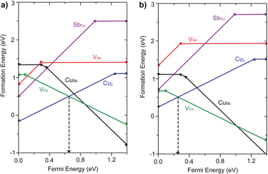
The p-type conductivity of the copper chalcogenides is generally rationalized in terms of the provision of an excess of the volatile components (e.g., Sb and a chalcogen) that would encourage the formation of copper vacancy acceptors. However, density functional theory is helpful in confirming this in a more systematic way. A good example is the work of Xue 2015 who evaluated the energetics of the full set of vacancies, interstitials, and antisites for CuSbSe2.Reference Xue, Yang, Yuan, Wang, Liu, Zhou, Hu, Pan, Chen and Tang14 Of these, VCu and CuSb are acceptors and Cui, VSe, and SbCu are donors. Figure 9 shows how the energy of the defects varies as a function of the Fermi level position for the cases of Se-poor and Se-rich conditions. In Sb-rich conditions, the most easily formed defects are VCu acceptors and Cui donors, and it is the position of their balance point that determines the Fermi level position. In the case of Se-rich growth, the formation of VCu is encouraged and their population grows, decreasing the Fermi level—but at the same time increasing the formation energy for VCu until it is equaled by that of Cui when E F = 0.2 eV. Here, the formation energy of VCu is 0.5 eV and at 300 °C, this would equate to p = 1018 cm−3. This is consistent with experimental findings. On the other hand, when growth is conducted under Se-poor conditions, the formation energies of VCu and Cui are more closely matched, and their densities become equalized near the mid-gap point. Hence the donors would compensate the acceptors and the material would be expected to be intrinsic. Xue concludes by noting that the native defects in CuSbS2 and CuSbSe2 are not expected to be deep, and hence would not cause recombination problems. Nevertheless, as will be seen later, recombination losses are serious in these materials, but this is at least partly due to the control of the width and position of the depletion region. A similar theoretical study showing the prevalence of copper vacancies in CuSbS2 is reported by Yang et al. Reference Yang, Wang, Han, Zhou, Song, Chen, Zhong, Lv, Niu and Tang137
CuSbSe2 defect chemical potentials determined by density functional theory calculationsReference Xue, Yang, Yuan, Wang, Liu, Zhou, Hu, Pan, Chen and Tang14 for Se-poor (a) and Se-rich (b) growth conditions. For both, the lowest energy defects are VCu and Cui and Xue considers that the Fermi level is determined by their balance point. In the case of Se-rich material (b), the density of VCu increases from left to right until it is matched by Cui—at this point the carrier density due to vacancies is estimated as p = 1018 cm−3. Such high carrier concentrations are observed in practice. Figures reproduced from Xue, 2015Reference Xue, Yang, Yuan, Wang, Liu, Zhou, Hu, Pan, Chen and Tang14 with permission from John Wiley.
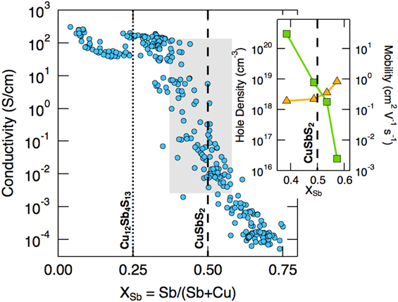
Experimentally it is also found that for CuSbS2, the Sb/(Sb + Cu) ratio influences both the carrier concentration and mobility, but oppositely, as shown in Fig. 10.Reference Welch, Zawadzki, Lany, Wolden and Zakutayev58,Reference Zakutayev, Baranowski, Welch, Wolden and Toberer177 While a deficiency of Cu (Sb excess) increases the carrier concentration (i.e., the population of VCu) as expected, the hole mobility rises faster as the Sb is depleted (Cu excess)—the Sb-poor samples have the highest conductivity, as shown in the figure. Welch goes on to consider the effect of Sb-rich, Cu-poor and Sb-poor, Cu-rich compositions.Reference Welch, Baranowski, Peng, Hempel, Eichberger, Unold, Lany, Wolden and Zakutayev212
Conductivity versus antimony metal fraction for the Cu–Sb–S system, showing the positions of CuSbS2 and Cu12Sb4S13. The inset shows the hole density and carrier mobility in the vicinity of the stoichiometric CuSbS2 position. Cu-poor compositions encourage the formation of VCu and hence increase p-type carrier concentration, but the mobility (inset) decreases slightly. Figure reproduced from Welch, 2015Reference Welch, Zawadzki, Lany, Wolden and Zakutayev58 with permission from Elsevier. See also Zakutayev, 2014.Reference Zakutayev, Baranowski, Welch, Wolden and Toberer177
Note on ionic conduction
As mentioned in the introduction, PerniuReference Perniu, Duta and Schoonman5 used the Kroger–Vink methodology to make a paper assessment of the possibility of ionic conduction in CuSbS2. From the standpoint of PV devices, which operate in dc conditions, the exposure to a continual field having the same polarity could cause electromigration which could be harmful to the stability of PV devices. Indeed, the once promising Cu2S–CdS solar cell ultimately failed to get to market on account of Cu-related instability. Experimentally, ionic conduction on the mobile Cu sublattice has been seen to operate at higher temperatures (T > 122 °C in Cu3SbS3, and T > 135 °C Cu3BiS3Reference Makovicky63). While PV devices might not be expected to reach these temperatures in service, this does point to an increasing tendency to instability of the Cu, at least for these materials. This should be explored further by experiment in those compounds in the series that may be of interest for PV applications.
Missing nanoparticles and missing nanosolar cells
A comprehensive list of the reports of the formation of ‘nano-’ and other particles from the Cu–Sb- and Cu–Bi-chalcogenides is presented in Table 9. Despite there being about 70 reports, there are some surprising omissions from the literature. First, there are comparatively few reports of making actual solar cell devices with nanoparticles (there is one quantum dot device, two attempts at dye sensitized solar cell (DSSC) structures, and some controversial some spun film-made devices—for a full commentary see the section titled “synthesis methods for nanoparticles”). Second, to the author’s knowledge, quite a number of the family members of this chemical class have not yet been synthesized in the form of nanoparticles (Table 9). The sulfides are quite well represented (excepting CuBiS2 and Cu12Bi4S13) but only two of the selenides have been synthesized (CuSbSe2 and Cu3SbSe3) and none of the tellurides. The entire row of CuBiX2 analogues remain to be made, and the bismuthic tetrahedrites Cu12Bi4X13, are also entirely absent.
Finally, it may be of interest to synthetic chemists that Cu4Bi4X9 has been made by the solvothermal method but not by hot injection while for the reverse is true for Cu12Sb4S13 and CuSbSe2.
Synthesis methods for nanoparticles
‘Solvothermal’ and ‘hot injection’ synthesis methods are equally popular. The next most-reported methods, ‘chemical bath’ and ‘thiocarbamate’ routes, each have a factor of three fewer reports and others have been attempted just one or two times each. A summary of the methods follows:
Solvothermal synthesis
Copper, antimony, and bismuth present as chlorides, nitrates, or sulfates (occasionally others) are reacted with a chalcogen source, most often L-cystine for S (but occasionally thiourea, thioglycolic acid, or sulfur). Details of the variations reported and the protocols for other chalcogens are listed in Table 8.
Synthesis and properties of particles: microparticles, nanoparticles, powders, micro- and nanorods, and similar structures.
CBD—chemical bath deposition.
DDT—1-dodecanethiol.
DETA—diethylenetriamine.
ODA—octadecylamine.
ODE—1-octadecene.
TEG—triethelene glycol.
TEGA—triethylenetetramine.
† Bandgap value is unreliable.
Hot injection
This method is equally popular as the solvothermal methods. Copper, antimony, and bismuth are supplied as acetates, acetylacetonates (acac), chlorides, or nitrates and reacted most usually with elemental sulfur in solution with oleylamine, but other sulfur sources and solvents/mixed solvents have been reported, as shown in Table 8. 1-dodecanethiol is popular.
Thermal decomposition of thiocarbamates
Since metal thiocarbamates such as Bi(S2CNEt2)3 and Cu(S2CNEt2)2 are a single source of both a metal and S, their thermal co-decomposition in a suitable solvent provides an opportunity for synthesis of the ternaries. As listed in Table 8, this has been demonstrated for CuSbS2,Reference Xu, Shen, Zhang, Gu and Wang213 Cu3SbS3,Reference Xu, Shen, Zhang, Gu and Wang213 Cu12Sb4S13,Reference Xu, Shen, Zhang, Gu and Wang213 Cu3BiS3,Reference Deng, Shen, Zhang, Xu and Wang214,Reference Zhou, Ma, Zhang, Wang, Chen, Huang and Yu215 and Cu4Bi4S9.Reference Deng, Shen, Zhang, Xu and Wang214 Manipulation of the solvent choice can be used to tune the particle size, e.g., Deng 2014Reference Deng, Shen, Zhang, Xu and Wang214 changed the size and morphology from sheets (1 μm; 1.29 eV) to particles (25 nm; 1.35 eV) for Cu3BiS3 and recorded a corresponding change in band gap, presumably from quantum confinement (Table 8).
Chemical bath deposition-like reactions
Thermal decomposition of thiourea in the presence of the metal ions, usually in aqueous solution. The method was first developed by KaurReference Kaur and Chopra216 for the formation of CdS films and is well-known. Films deposit on any surfaces in contact with the solution while the liquor itself contains nanoparticles.
Chemical conversion reactions applied to nanoparticles having a related composition
There are two reports only, and they use different methods:
GuriaReference Guria, Prusty, Chacrabarty and Pradhan217 made Cu3SbS3 nanorods by converting Sb2Se3 nanorods using CuCl2. They made monodisperse rods 30 × 300 nm and up to 3 μm long and having an optical band gap of 1.04 eV. Interruption of the exchange process enabled core–shell structures to be made.
SenevirathnaReference Senevirathna, Werrett, Pai, Blair, Spiccia and Andrews218 did a double conversion—Bi2O3 was converted to the sulfide using aryldithioic acid and then to Cu3BiS3 using CuCl. This formed agglomerated particles 70–80 nm in size.
Direct mechanical milling of the ternary compound
Powderization is not popular: there are just two reports. Zhang made 5 nm particles of CuSbS2.Reference Zhang, Xu and Tan219 Marino ball milled it down to <1 μm.Reference Marino, Block, Pottgen and Villevieille220
Iodine vapor transport
There is a single report. Cu4Bi4S9 was transported in iodine vapor to generate rods 10–1500 nm in diameter and 0.1–10 μm in length.Reference Kryukova, Heuer, Doering and Bente221
Phase and shape control in nanoparticle synthesis
It is a remarkable feature of nanocrystal synthesis that the reaction conditions may be selected to reproducibly control the material’s phase. Whereas for the thin film methods, phase pure materials are difficult to achieve (see above), and it has been shown repeatedly that, for example, all four phases of Cu–Sb–S can be obtained. While the earliest nanoparticle papers reported single compounds (CuSbS2Reference Su, Xie, Wan, Li and Qian222; Cu3SbS3Reference Wang, Yue, Fan and Yan223; Cu3SbS4Reference van Embden and Tachibana224; and Cu12Sb4S13Reference van Embden, Latham, Duffy and Tachibana225), some later papers present the full range of systematic reaction conditions required to collect the whole set. For example, RamasamyReference Ramasamy, Sims, Butler and Gupta226 made all four phases of Cu–Sb–S by hot injection and was able to select the product by controlling the temperature, Cu/Sb ratio and the mix of thiols used. Figure 11 shows the full set of TEM images, lattice images, and XRD patterns (this is consistent with a report by Ikeda, also for hot injectionReference Ikeda, Sogawa, Tokai, Septina, Harada and Matsumura227).
Nanoparticles of the full set of Cu–Sb–S phases that have been selectively synthesized by the hot injection method. Phase control was achieved by selection of the temperature, Cu/Sb ratio, and the mixture of thiols used.Reference Liang, Huang, Ren, Zhang, Xie and Feng228 Left to right by columns: (a–c) Cu3SbS4, (d–f) Cu12Sb4S13, (g–i) CuSbS2, and (j–l) Cu3SbS3. Top row—bright field TEM images, middle row—HRTEM lattice images, bottom row—XRD patterns. The XRD and the HRTEM confirm the phase purity of the nanoparticles. This quality is not achievable for thin film synthesis of the same materials. Figure from Liang et al., 2016Reference Liang, Huang, Ren, Zhang, Xie and Feng228 with permission from the Royal Society of Chemistry.

Nanoparticles in this class of compounds express the full range of shapes that may be imagined, including spheres, bricks, sheets, wires, and stellated structures. Some synthesis conditions allow the particles to assume the crystal habits observed in nature. For example, natural deposits of chalcostibite CuSbS2 resemble the nanobricks and sheets shown in Fig. 12 and reported by ZhangReference Zhang, Zhou, Liu, Li, Lai and Jia229 and Ramasamy.Reference Ramasamy, Gupta, Sims, Palchoudhury, Ivanov and Gupta230 Tailoring of the reaction conditions, for example, by substituting antimony acetate for the chloride, can switch the nanoparticle’s crystal habit (see Fig. 12, for example). In addition, it is possible to template structures, for example, by the use of anodic aluminium oxide, as demonstrated by the oriented columnar CuSbS2 structures in Fig. 12 (lower right).
Nanoparticle shapes achievable for CuSbS2 grown under different conditions. Top row: d, h, and l from the original figure in Ref. Reference Ramasamy, Gupta, Sims, Palchoudhury, Ivanov and Gupta230 showing top, side, and HRTEM views of CuSbS2 nanoplates grown by hot injection from SbCl3, Cu(acac)2 and 1-oleylamine with sulfur. Reproduced with permission from Ref. Reference Ramasamy, Gupta, Sims, Palchoudhury, Ivanov and Gupta230 originally published by the Royal Society of Chemistry. Bottom left: CuSbS2 ‘nanobricks’ formed by hot injection with copper acetylacetonate (Cu(acac)2), antimony acetate (Sb(Ac)3), oleylamine and sulfur. From Zhang 2013Reference Zhang, Zhou, Liu, Li, Lai and Jia229 originally published by ESG, Belgrade. Bottom right: CuSbS2 nanowires grown on an anodic oxide template using the solvothermal method from CuCl2, potassium antimonyl tartrate trihydrate, sulfur + diethylenetriamine. The template has encouraged the oriented growth. From Shi, 2015Reference Shi, Li, Wu and Dai189 with permission from Elsevier.

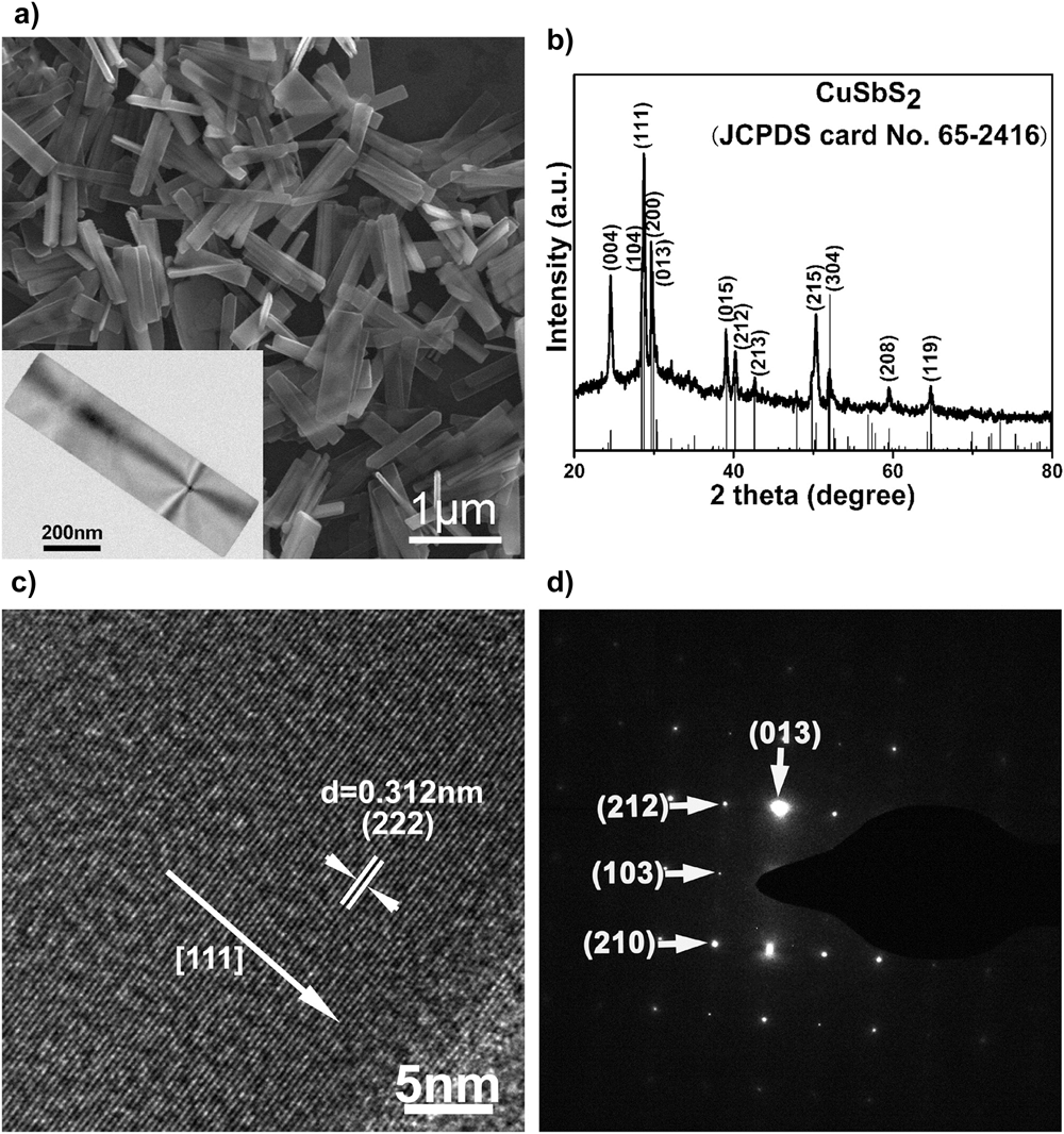
A most striking example is that of ‘tetrahedrite’ (Cu12Sb4S13) named for its distinctive crystal habit, and this being replicated on the 30 nm scale as shown in Fig. 13.Reference Xu, Shen, Zhang, Gu and Wang213 Very often though, the shapes of the particles are not so plainly crystallographic with spheres and stellated structures are common.
Nanoparticles of Cu12Sb4S13 (‘tetrahedrite’) synthesized by thermal decomposition of copper diethyldithiocarbamate and antimony diethyldithiocarbamate. (a) Bright field TEM—the tetrahedra characteristic of macroscopic mineral deposits are clearly visible on the 30 nm scale, (b) confirmation of the XRD crystal structure, (c) HRTEM confirming the d 220 and d 222 interplanar spacings, and (d) transmission electron diffraction pattern of the assembly. Reprinted with permission from Xu et al., 2013.Reference Xu, Shen, Zhang, Gu and Wang213 Copyright (2013) American Chemical Society.
PV devices—predictions of performance, design of devices, and technological status
Predictions of solar cell performance
There are several encouraging reports of predictions of the PCEs that should be achievable with compounds in the series, and these go above and beyond simply stating that the band gaps are appropriate. A summary is as follows:
(i) CuSbS2 and CuSbSe2: Yu et al.Reference Yu, Kokenyesi, Keszler and Zunger261 improve on the Shockley–Queisser estimate of efficiency by including recombination and optical absorption losses—the so-called spectroscopically limited maximum efficiency (SLME). They estimate maxima for CuSbS2 (23%) and CuSbSe2 (27%)—see also review by Ganose.Reference Ganose, Savory and Scanlon262 TableroReference Tablero207 gives a higher estimate for CuSbS2, with radiationless recombination suppressed, but it is not so realistic.
(ii) Ternaries CuSb(Se1−xTex)2 and CuBi(S1−xSex)2: Chen and PerssonReference Chen and Persson203 predict performance of the quaternary alloys CuSb(Se1−xTex)2 and CuBi(S1−xSex)2 having determined their band gaps and optical absorption spectra using DFT with HSE06. The direct gaps decrease with increasing x as expected and the PCEs were determined as a function of the composition and thickness of the absorber layers. For CuSb(Se1−xTex)2, the direct gap decreased from 1.43 to 1.07 eV as x was varied from 0 to 1, while the maximum efficiency peaked at 28.3% for x = 0.75 (thickness = 200 nm). For the same thickness of CuBi(S1−xSex)2, the gap decreased from 1.30 to 1.07 eV while the efficiency increased from 20.3% to a peak for x = 1 at 24.3%. Auger losses were predicted to reduce these values by ∼4% for heavily doped samples. The authors point out that since these compounds are highly absorbing, devices with absorbers in the range 50–200 nm should be viable.
(iii) Cu3SbS3: TableroReference Tablero263 estimates the high concentration performance of isoelectronically doped Cu3SbS3:O to be >40%, and in another publicationReference Tablero264 ∼43%; isoelectronic doping with O may help. The model is similar to that in Ref. Reference Luque and Marti265.
(iv) CuBiS2: In a model with radiationless recombination suppressed, TableroReference Tablero207 predicts efficiencies of ∼40% under AM1.5 illumination, which is unrealistic of course.
(v) Cu3BiS3: MesaReference Mesa, Ballesteros and Dussan266 reports a wxAMPSReference Liu, Sun and Rockett267 model of a Cu3BiS3 device giving V oc = 0.712 V, J sc = 36.25 mA/cm2, FF = 79.54%, and efficiency = 19.86%. The heterostructure partner is not named.
Device architectures
The most widely used device architectures used for these chalcogenides are now described:
‘Substrate’ and ‘superstrate’ (with comparison to normal and inverted as used in organic PV)
The two most commonly used device architectures for thin film PV are shown in Fig. 14. Both have been used for CuSbS2 and the related compounds.
Thin film PV device designs. (a) ‘Substrate’ design used for CIGS and CZTS and (b) the ‘superstrate’ design used industrially for CdTe. The two designs uphold the same sequence of films, i.e., TCO/n-type/p-type/contact, and differ only in their relationship to the support glass: for ‘substrate’ cells, the light passes only thought the TCO and the window layer, whereas for ‘superstrate’ cells, the light also passes through the glass. For reference, the sequence of layers in the figures is commensurate with the so-called ‘inverted’ design used in organic PVs. Both types of device configuration have been used for copper antimony sulfide-based solar cells.
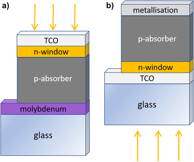
In the ‘substrate’ design (as used for CIGS), the films are deposited on an opaque substrate, in the sequence: opaque substrate/p-absorber/n-window/n-type transparent electrode (light enters through the latter). In the ‘superstrate’ design (as used for CdTe), the light enters through the glass and the design is named for its orientation in service. The n-type transparent electrode layers (transparent conducting oxides or TCOs) are deposited on the glass, followed by the n-type window, and the p-type absorber and its metallization. Hence the two differ in their relationship to the support glass, rather than in the sequence of layers, which is the same in both. For reference, this sequence—TCO/n-type/p-type/metal—is referred to in the organic PV community as the ‘inverted’ design, with the analogues of p-type being ‘hole selective’ or ‘anode layer’ and the n-type being ‘electron selective’ or ‘cathode layer’.
DSSC-like solar cells using nanoparticles
There is a large sub-genre of the PV literature in which the ruthenium dye in DSSCs is replaced by some other substance. For almost all absorber choices, these devices perform less well than the dye in Gratzel’s original design. The single exception is ‘perovskites’ for which there has been both global publicity and efficiencies greater than 20%. All the others fail to outperform standard DSSC devices, including those few that use CuSbS2. For example, Ramasamy’s cellReference Ramasamy, Tien, Archana and Gupta233 achieved ∼3%—far less than the 10–11% achieved for conventional DSSC. Han’sReference Han, Jia and Wang238 DSSC device with CuSbS2 has the novelty that the electrolyte hole transporter is based on polysulfides rather than the more usual I−/I3−. In a rare report of any kind of working device from Cu3BiS3, YinReference Yin and Jia268 reports 1.28% (I2/KI with Pt sensitized electrode). Overall there is no evidence at present to suggest that the use of this family of compounds in DSSC-like geometries will achieve high efficiency devices.
Device results by absorber type
Table 10 shows the device performance results for every device made from the whole class of compounds at the time of writing and listed in the order of absorber type.
These have been measured on small area contacts, typically ∼0.1 cm2, this being typical for technologies in development and somewhat less than the 1 cm2 minimum required for verifiable performance records. For these small devices, the errors in efficiency measurement may be expected to be greater than the ±0.2% or so expected for standardized test data.
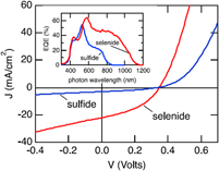
Devices with CuSbS2 absorbers (including difficulties with using n-CdS window layers)
The three highest performing CuSbS2 PV devices have efficiencies of between 3.1 and 3.2% making them identical within experimental error: Ikeda,Reference Ikeda, Iga, Septina, Harada and Matsumura154,Reference Septina, Ikeda, Iga, Harada and Matsumura269 Choi,Reference Choi, Yeom, Ahn and Seok144 and Banu.Reference Banu, Ahn, Ahn, Yoon and Cho146
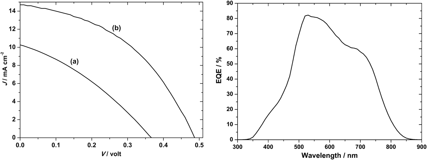
Those of Ikeda and Banu share the same ‘substrate’ device geometry and will be discussed first. Since the performances are comparable, there is no obvious advantage in the use of one deposition technique over the other (H2S sulfurization of metals or sulfurization of spun metal acetates). However, the conversion efficiencies are low and have not been bettered. The shortfall lies in the low J sc values—there is current loss in these devices. The V oc and FF values are respectable for prototype devices, but the current—normally the easiest parameter to increase—is low. Indeed, the deficit in J sc is reflected in the experimental external quantum efficiency (EQE) curves (see Fig. 15). Most authors show curves similar to the one in Fig. 15: there is a (relatively low) peak at about 520 nm—its left flank corresponds to the onset of absorption by the CdS window layer (its band gap corresponds to about 510 nm). In common with the CdTe/CdS solar cell, this absorption is parasitic and does not contribute to the photocurrent. As expected, there is no photocurrent above 830 nm, the band gap of CuSbS2. Between the peak and 830 nm, the EQE is diminished, and this has been attributed to recombination losses in the absorber itself.Reference Welch, Baranowski, Lucas, Toberer, Wolden and Zakutayev270
CuSbS2 device characterization results for a substrate design glass/Mo/CuSbS2/CdS/ZnO:Al solar cell. Ikeda’s best device (curve b, left-hand panel)Reference Ikeda, Iga, Septina, Harada and Matsumura154,Reference Septina, Ikeda, Iga, Harada and Matsumura269 performed with V oc = 490 mV, J sc = 14.7 mA cm2, FF = 44% and had an efficiency of 3.1%. The EQE is shown in the right-hand panel. To the left of the peak at 520 nm, there is EQE loss that corresponds to parasitic absorption in the n-CdS ‘window’ layer. Between ∼550 and 750 nm, the loss is attributed to recombination.Reference Welch, Baranowski, Zawadzki, Lany, Wolden and Zakutayev180 Figure from Septina, 2014Reference Septina, Ikeda, Iga, Harada and Matsumura269 reproduced with permission from Elsevier.
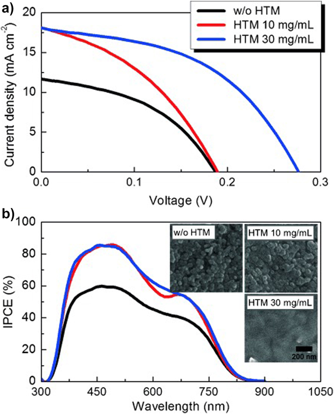
Further confirmation of the optical loss due to CdS window layers may be seen by comparison with the EQE curves reported for cell designs that do not contain it. For example, Choi’s cellReference Choi, Yeom, Ahn and Seok144 (Fig. 16) has a DSSC design in which the light enters through coated glass and TiO2 (there is no CdS). Accordingly, the EQE values hold up between 450 nm and the lower limit of ∼325 nm (the onset of absorption in the glass and the transparent electrode).
Device performance results for a DSSC design of CuSbS2 solar cell comprising glass/FTO/compact TiO2/mesoporous TiO2/CuSbS2/PCPDTBT/Au.Reference Choi, Yeom, Ahn and Seok144 (a) The best device performed with V oc = 304 mV, J sc = 21.5 mA.cm2, FF = 47% and had an efficiency of 3.1%. (b) Since this design has no CdS window layer, the EQE (here called ‘incident PCE’) holds up below 500 nm and the current is raised to 21.5 mA/cm2 from the lower level of 15–16 mA cm2 reported for conventional heterojunction devices with CdS. Figure from Choi, 2015.Reference Choi, Yeom, Ahn and Seok144 Reproduced with permission from John Wiley.
There is a further complication from using CdS: of the 24 reports of CdS/CuSbS2 devices, half have the ‘substrate’ and half the ‘superstrate’ design. However, the ‘substrate’ ones outperform the ‘superstrate’ ones with 92% of the former and only 33% of the latter exceeding 1% efficiency. This difference is caused by diffusion of Cu into the CdS—in ‘substrate’ cells, the CdS is an overlayer, while in ‘superstrate’ ones, it is buried beneath the CuSbS2 and therefore susceptible to diffusion during thermal processing. Cu is known to poison CdS by introducing a deep hole trapReference Claybourn, Brinkman, Russell and Woods271—it is the same effect that made the extensive development of the CuxS—CdS device fail in the 1980s.
Evaluation of the band line-ups for CdS with CuSbS2Reference Lucas, Welch, Baranowski, Dippo, Hempel, Unold, Eichberger, Blank, Rau, Mascaro and Zakutayev179 indicates a sharp ‘cliff-like’ step which LucasReference Lucas, Welch, Baranowski, Dippo, Hempel, Unold, Eichberger, Blank, Rau, Mascaro and Zakutayev179 points out is linked to high levels of recombination and low V oc. Indeed, temperature-dependent measurements gave a 0 K value of V oc = 0.7 V, which is smaller than for mainstream thin film technologies. Lucas concludes that CdS is unlikely to be a good heterojunction partner for CuSbS2.
However, efforts to replace the CdS in conventional planar devices with alternative window layers have not met with success: PeccerilloReference Peccerillo152 evaluated the band line-ups with ZnS, ZnSe, and ZnTe with CuSbS2 and found them to be favorable before embarking on a program of making and testing both substrate and superstrate designs of devices. The CuSbS2 was formed by sulfurization of sputtered metals. The film properties were typical for the material (optical band gap 1.45 eV, p = 1.5–3.5 × 1017 cm−3, mobility 6–13 cm2/(V s), resistivity 2–4 Ω cm). Spurious above-gap photoluminescence was identified by XPS as being due to oxides and efforts were made to remove any Sb2O3 by etching. The result was that none of the trial devices achieved efficiencies greater than the CdS device, i.e., none exceeded ∼1%.
LucasReference Lucas, Welch, Baranowski, Dippo, Hempel, Unold, Eichberger, Blank, Rau, Mascaro and Zakutayev179 focused on making improvements to the CuSbS2 absorber layer itself by thermal treatment in the presence of Sb2S3 which was effective in protecting against both Sb and S loss and phase decomposition. This had the effect of increasing the carrier lifetime from 0.5 to 0.7 ns. There was a concomitant rise in V oc from 121 to 350 mV, but the low value of J sc was still the limiting factor (up to 5.20 from 3.31 mA/cm2) and hence the efficiency increased from 0.113 to 1.02%.
This is a common research outcome for CuSbS2: many authors give credible accounts of efforts to improve the material preparation (film growth, second phase elimination) and device fabrication, only for their work to hit a rather low ceiling (1 or 2%) in device efficiency. Despite their being 20–30 published accounts of devices, few provide evidence of the physical mechanisms that are so evidently limiting the performance. In particular, with the exception of Lucas,Reference Lucas, Welch, Baranowski, Dippo, Hempel, Unold, Eichberger, Blank, Rau, Mascaro and Zakutayev179 there are no published reports of carrier lifetime (e.g., time resolved photoluminescence), none of the energies and capture cross sections of the carrier trapping levels that mediate recombination (e.g., by deep level transient spectroscopy) and none of direct measurements of the electrical junction position [e.g., by electron beam induced current (EBIC)]. Each of these could provide some insight into how to improve the device performance. There are some insights to be gained by comparison with CuSbSe2 (see below), but overall it may only be said that CuSbS2 is a difficult material and that progress in developing its PV devices has hit a roadblock.
Devices with Cu3SbS3, Cu3SbS4, and Cu12 Sb4S12 absorbers
There is one report for each of these three compounds: Cu3SbS3,Reference Maiello, Zoppi, Miles, Pearsall and Forbes26 Cu3SbS4,Reference Franzer, Paudel, Xiao and Yan65 and Cu12Sb4S12.Reference Wang, Yang, Xia, Leng, Zhou, Xue, Zhong, Gao, Song and Tang141 Only Cu3SbS4 comes close to performance at the 0.5% level, and the other compounds lag behind by a factor of ten at least. Presumably similar problems to those of CuSbS2 (above) are compounded by the paucity of studies.
Devices with CuSbSe2 and CuSb(Se,S)2
While the band gap of CuSbSe2 (1.1 eV) is lower than that of CuSbS2 (1.49 eV), it is still in the peak region of the Shockley–Queisser performance/band gap curve, and despite there being few reports of devices, progress has been relatively rapid. Having developed a co-sputtering route for 1% CuSbS2 cells (using MoOx back contacts), WelchReference Welch, Baranowski, Lucas, Toberer, Wolden and Zakutayev270 translated the same growth conditions and structure to CuSbSe2 directly and obtained ∼3% efficiency—the J–V and EQE results for both structures are compared in Fig. 17. The enhanced current collection in the Se-device is seen in the differences between the EQE curves—that for CuSbSe2 is extended in wavelength due to the lower band gap and is also higher. WelchReference Welch, Baranowski, Zawadzki, Lany, Wolden and Zakutayev180 attributes the sharp peak in EQE for both devices as corresponding to generation and drift collection in the depletion region of the device itself. C–V measurements indicate that the depletion region itself is narrow (135 nm at zero bias). To the right of the peak, the EQE is diminished by recombination, i.e., carrier diffusion is limited by short diffusion lengths and short minority carrier lifetimes. Indeed, the lifetimes were measured for CuSbSe2 as τe = 190 ps (using optical pump Terahertz probe spectroscopy—OPTP at 805 nm). This is short in comparison to mainstream thin film semiconductors for which ns timescales are more common. Further insight to the factors limiting device performance were obtained using a combinatorial experiment in which the ratio of Cu2Se and Sb2Se3 supplied to the substrate varied with position, allowing the effects of composition on device performance to be systematically explored—as shown in Fig. 18. Slightly Cu-poor compositions work best, and there is a dramatic drop-off in performance as the Cu-rich threshold is crossed. Moreover, while this material is expected to be highly conductive (see section “Formation and properties of bulk, thin film and nanoparticle materials”), the local flux ratio [Sb2Se3]/[Cu2Se] has been shown to control the carrier density by manipulating the population of VCu. So, while the photocurrents obtained are limited by the narrow depletion regions, when the depletion region is expanded by decreasing the carrier density, this has the unwanted effect of reducing the band bending and hence reducing V oc. The reviewer speculates that expansion of the field region by adopting a p–i–n junction may be necessary to increase performance more effectively.
A comparison of similar ‘substrate’ geometry CuSbS2 and CuSbSe2 devices. WelchReference Welch, Baranowski, Lucas, Toberer, Wolden and Zakutayev270 optimized a co-sputtered CuSbS2 device and then created a CuSbSe2 under similar conditions for comparison. There is a significant difference in current collection, with the lower gap of the selenide (1.1 eV) extending the collection beyond that of the sulfide (1.45 eV). Both show a sharp peak in EQE attributed to drift of carriers excited in a narrow depletion region. However, the EQE on the right flank is higher for the selenide, implying that the recombination losses in the sulfide are higher. The structure is glass/Mo/MoOx/CuSbS2/CdS/i-ZnO/AZO/Al (and its Se analogue). Figure from Welch, 2015,Reference Welch, Baranowski, Lucas, Toberer, Wolden and Zakutayev270 with permission from IEEE.

CuSbSe2 (a) device results and (b) EQE for material formed in a combinatorial experiment by co-sputtering Cu2Se and Sb2Se3.Reference Welch, Baranowski, Zawadzki, Lany, Wolden and Zakutayev180 The highest performance was Cu-poor material, with Cu-rich material causing a significant drop-off in performance. Figures reproduced from Welch et al, 2015Reference Welch, Baranowski, Zawadzki, Lany, Wolden and Zakutayev180 with permission from the Japan Society of Applied Physics. Copyright 2017 The Japan Society of Applied Physics.
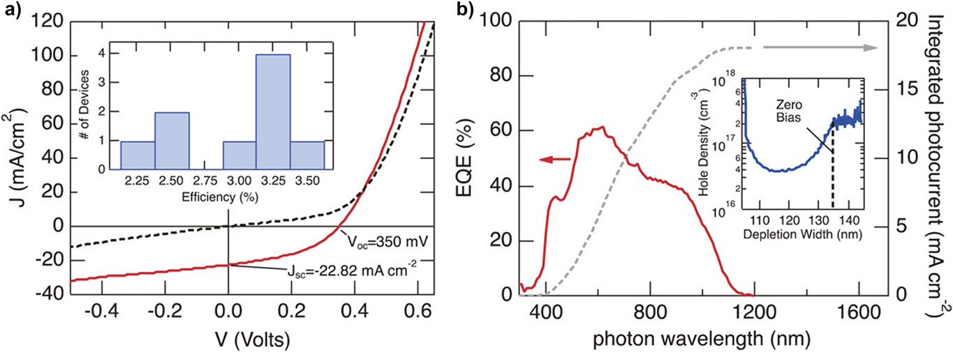
Both the direct comparison between CuSbS2 and CuSbSe2 devices,Reference Welch, Baranowski, Lucas, Toberer, Wolden and Zakutayev270 and the fact that the selenide has achieved higher efficiencies with five times fewer papers imply that CuSbSe2 has some advantage. Recombination appears to be lessened. However, comparison of the limited studies of minority carrier lifetimes (τe = 190 ps—selenide; τe = 500–700 ps—sulfide), would suggest that the sulfide should give superior performance—but this has not been achieved at present. Further lifetime measurements and device fabrication would be necessary to clear up this point.
YangReference Yang, Wang, Yuan, Chen, He, Song, Ding, Zhao and Tang142 provides the only report to date of a mixed sulfo-selenide device, with 4% S, and achieved 2.7%. Its voltage and current were comparable to the best CuSbSe2 ones, but it was let down by a poor fill factor (36%) and a high reverse bias leakage current (i.e., low R shunt—value not reported). Improving the material integrity would allow this to be improved upon. It would be valuable to explore a wider range of compositions of CuSb(S,Se)2 so as to determine whether the voltage–current combination could be optimized, and whether there are any systematic variations in recombination behavior.
Devices with Cu3SbSe3, Cu12Sb4Se13, and Cu–Sb–Te compounds
There are no reports to the author’s knowledge.
Devices with CuBiS2
There is just a single report of its use in solar cells,Reference Suriyawong, Aragaw, Shi and Lee272 that being for a CuBiS2 quantum dot sensitized DSSC with a polysulfide electrolyte and trials of various electrode types on the liquid side. Probably, researchers are discouraged from making further devices (e.g., thin film structures) on account of the band gap of 1.61 eV, which is slightly higher than is usually sought for single junction PV. Nevertheless, this is the ideal gap for forming a tandem device with silicon (1.1 eV).
Devices with Cu3BiS3
Given that Cu3BiS3 is the second most researched compound in the family after CuSbS2, and that 75% of the papers on it mention solar PV, it is a surprise that there is just one report of a working device.
Mesa reports an electron microscopy study of a substrate-geometry device, but it was not photoactive.Reference Mesa, Dussan, Sandino and Lichte273 In other work, solution growth of the compound into a dye cell structure yielded 1.28% conversion efficiency, a respectable voltage of 448 mV, an excellent fill factor (61%), but was let down by a low photocurrent of 4.5 mA/cm2.
Further studies of the roles of heterojunctions and grain boundaries in Cu3BiS3 are reported by Mesa,Reference Mesa, Chamorro, Vallejo, Baier, Dittrich, Grimm, Lux-Steiner and Sadewasser116 who measured the surface electronic properties of NH3-cleaned Cu3BiS3 films and also with overlayers of CdS, ZnS, and In2S3 using Kelvin probe microscopy and surface photovoltage measurements. While the grain boundaries in the Cu3BiS3 itself were found to be positively charged, a different behavior was seen when there was an over-layer of either CdS or In2S3 (but not ZnS): the more positive work function at the positions of the grain boundaries in the underlying Cu3BiS3 was taken as evidence that the over-layers changed the grain boundary charge state from negative to positive. Further contact potential difference (CPD) measurementReference Mesa and Fajardo117 of grain boundary positions in clean and CdS-coated Cu3BiS3 was interpreted using Seto’s grain boundary model.Reference Seto274 For Cu3BiS3, they found the bulk p-type carrier concentration to be 3.86 × 1016 cm−3 with the grain boundary charge density (p-type) being 4.19 × 1011 cm−2 (reduced CPD at the grain boundaries). For the CdS over-layer, the bulk carrier concentration was found to be 2.9 × 1016 cm−3 with the grain boundary charge density (negative) being 3.2 × 1011 cm−2 (increased CPD at the grain boundaries). Overall, the authors considered CdS and In2S3 as being able to invert the charge of underlying grain boundaries, but ZnS not.
The papers do not speculate on the reason for the zero and low device efficiencies reported. Fundamental experimental studies of the carrier lifetimes and of deep levels are absent from the literature. Certainly, devices from this material should be explored more thoroughly—its band gap of 1.40 eV should attract more interest. It is speculated anecdotally that further labs may have attempted to make devices but did not report them due to their very low performance. This is one instance where the reporting of negative results would have been useful to form an overview of the potential of Cu3BiS3 in PV.
Devices with Cu4Bi4S9
Crystallographic studies of Cu4Bi4S9 confirm it as a bona-fide phase even though it has no recorded Sb analogue. It has a thin film band gap of 1.14 eV, or 0.96 eV as the average reported for nanoparticles. This puts it at the low end of the Shockley–Queisser curve but it is potentially viable for PV applications. It appears to be readily produced in nanowire form (see above), and Liu and co-workers at Henan University, China, have exploited this by forming spun nanowire films to produce a remarkable set of device resultsReference Liu, Cheng, Wang, Zhang and Gu150,Reference Liu, Zheng, Zhang, Xiao and Wang195–Reference Wang, Liu and Gu200 —but not without stirring some controversy. The papers give clear accounts of the formation of ‘superstrate’ style devices, mostly grown on ITO-glass, and with some on FTO-glass. A wide range of intermediate layers were introduced between the TCO and the Cu4Bi4S9 nanowire film. These include In2O3, In2S3, ZnO nanowires, Zn2SnO4, and α-Fe2O3. The Cu4Bi4S9 nanowire film itself was variously infiltrated with reduced graphene oxide or else graphene nanosheets. The evolution of the devices has been rationalized with energy diagrams describing a cascade of electron (conduction band) levels from the absorber through the various intermediate layers. As shown in Table 10, the device results are remarkable and reach 10.9% for the glass/ITO/ZnO NW/Cu4Bi4S9-GN substrate geometry device shown in Fig. 19.
A ‘superstrate’ cell comprising a Cu4Bi4S9 (CBS in the figure) nanowire absorber loaded with graphene nanoplates, i.e., glass/ITO/ZnO NW/Cu4Bi4S9-GN. The authors claim 10.9% efficiency, V oc = 780 mV, J sc = 19.8 mA/cm2, and a fill factor of 71%, but not without stirring some controversy. (a) ZnO nanowires, (b and c) Cu4Bi4S9 + graphene SEM and TEM, and (d) cross section of the device structure. Figure from Liu et al, 2016;Reference Liu, Wang, Zheng and Gu199 used in accordance with the Creative Commons Attribution (CC BY) license (https://creativecommons.org/licenses/by/4.0/).
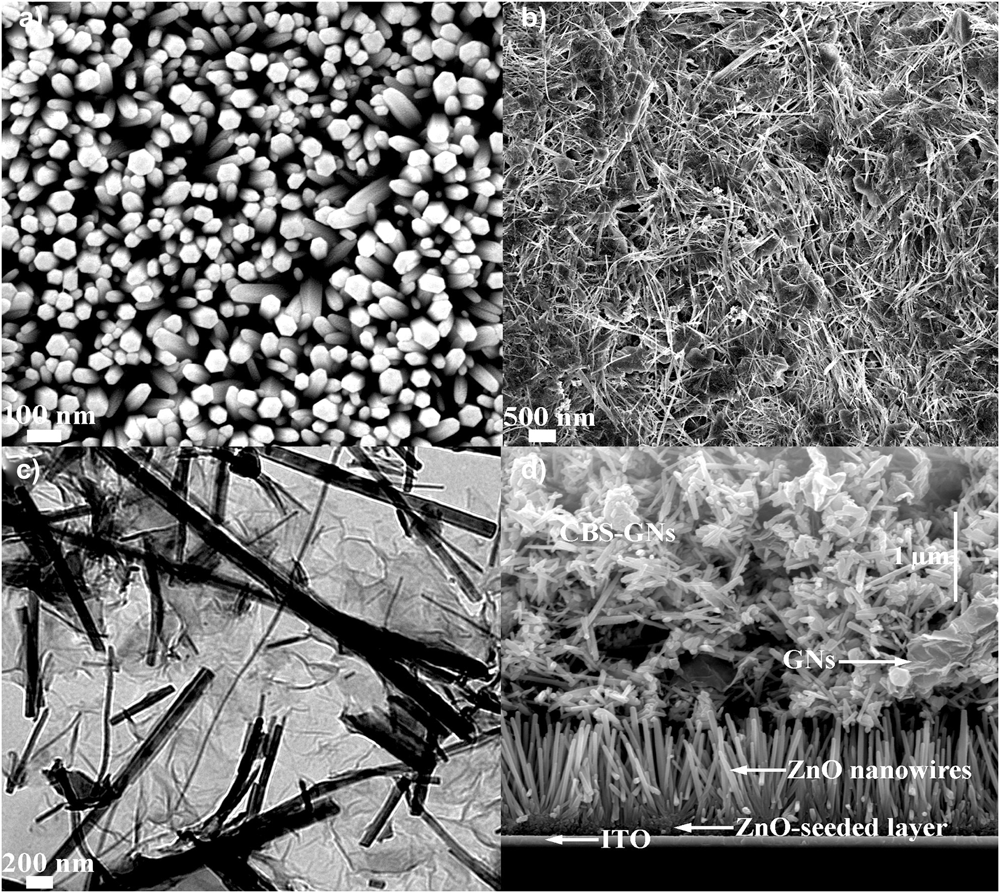
Criticism has arisen for several reasons. First, the V oc achieved (780 mV) is 70–80% of the band gap value, comparable to the best GaAs, even though the open network of Cu4Bi4S9 nanowires may be expected to give low shunt and high series resistances that make this voltage unlikely. Second, the data presented in the papers is unusual in that there are few J–V curves shown, and the photoresponse spectra are not shown in the conventional units of EQE. Third, only one group has achieved these results, and the papers do not report any independent testing. As is usual for any new technology in PVs, repetition of the device by another group and verification of the device performance result by an accredited test center would be helpful in this case. Until these actions are complete, unfortunately these results will be met with skepticism.
Devices with Cu12Bi4S13 and all other Cu–Bi–Se and Te compounds
There are no published reports to the author’s knowledge.
Summary of device performance achievements to date
Table 10 gives a comprehensive overview of all device results published at the time of writing.
Of the dozen or so compounds in the family with potential to be PV absorber materials, it is remarkable how few have been tested and demonstrated to function in laboratory-scale devices. From these, the most successful to date has been CuSbS2–CuSbSe2, with there being several independent reports of each having achieved efficiencies of greater than 3%. The high points are 3.22% for CuSbS2Reference Banu, Ahn, Ahn, Yoon and Cho146 and 4.7% for CuSbSe2.Reference Welch, Baranowski, Peng, Hempel, Eichberger, Unold, Lany, Wolden and Zakutayev212 Devices having the ‘substrate’ configuration (Fig. 14) in which the CdS window layer is not buried beneath the absorber, perform better—presumably since the CdS is not poisoned by Cu diffusion. Also, devices having CdS window layers are optically limited since absorption in the CdS does not generate carriers that are collected by the junction.
Devices have been made from Cu3SbS3, Cu3SbS4, Cu12Sb4S13, and CuBiS2, but they struggle to reach 0.5% PCE. While Cu3BiS3 is the second most researched material in the whole family, there is one single report of a working device made from it. This is a ‘dye cell’ type device having an I2–KI electrolyte—it achieved 1.28%.Reference Yin and Jia268 Within the context of research that seeks to improve on the original dye cell design by replacing the ruthenium-based dye with another absorber, the result is unremarkable: the original design achieves efficiencies of >10% and this does not represent an improvement. Conventional structures should be investigated. Finally, the apparently impressive results of up to 10.9% reported for Cu4Bi4S9Reference Liu, Wang, Zheng and Gu199 are not generally considered to be reliable and would certainly need to be verified in order for this to be confirmed as a significant direction for future research.
Other applications
Photocatalysis
The visible region band gaps of these compounds have generated some interest for hydrogen evolution and photoactivity tests with dyes, although there are few reports to date:
(i) CuSbS2: Reported for hydrogen generation with a CdS/Pt partner layer.Reference Zhang, Li, Li, Li, Zhang, Delaunay and Zhu156
(ii) CuBiS2: Photodegradation of dyes demonstrated for SiO2 nanospheres coated with TiO2 and with an outer layer of CuBiS2.Reference Abdullah and Kuo280–Reference Abdullah, Kuo, Lee and Wu282
(iii) Cu3BiS3: Hydrogen evolution under AM1.5 illumination was demonstrated for a Pt–In2S3/Cu3BiS3 electrode combined with a Pt electrode.Reference Kamimura, Beppu, Sasaki, Tsubota and Ohno163
Thermoelectrics
Since these compounds have mixed van der Waals and co-valent bonding, they have the potential for the high electrical and low thermal conductivity required for maximization of the dimensionless figure of merit (ZT) that indicates high thermoelectric performance. The highest ZT reported was for Cu12Sb(4−x)Bi(x)S13 (x = 0.2) ZT = 0.84,Reference Kumar, Chetty, Femi, Chattopadhyay, Malar and Mallik27 which is within the range of values reported for the classic thermoelectric, Bi2S3 (0.8–1), but reports for other materials in the family fall short of this—they are not prime candidates for thermoelectric applications. A summary is as follows:
(i) CuSbS2: Gudelli’s theoretical evaluationReference Gudelli, Kanchana, Vaitheeswaran, Svane and Christensen205 suggests that p-type will perform better than n-type, which is just as well since it is naturally p-type. Further theory from AlsalehReference Alsaleh, Singh and Schwingenschlogl283 highlights the role of interlayer coupling in thermal conductivity and also for CuSbSe2.
(ii) CuSbSe2: ZhangReference Zhang, Yang, Jiang, Fu, Xiao, Luo and Zhou88 increased ZT by a factor of 1.6 at 623 K, from 0.25 to 0.41 by introducing a small fraction of Cu3SbSe4 which acts to tune the conductivity since it affects both the carrier concentration and mobility.
(iii) Cu3SbSe3: KirkhamReference Kirkham, Majsztrik, Skoug, Morelli, Wang, Porter, Payzant and Lara-Curzio89 reports a minimum in thermal conductivity at 423–448 K of 0.3 W/(m K), associated with an order–disorder transformation. See later work by Samanta below. For nanoparticles, SamantaReference Samanta, Gupta, Kaur, Sharma, Pandey, Singh, Senguttuvan, Sharma and Bandyopadhyay67 reports a thermal conductivity ∼2.04 W/(m K) at 300 K reducing to 1.9 W/(m K) above 380 K where there is an order–disorder transformation and anharmonic behavior begins. WeiReference Wei, Wu, Sun, Pan and Li90 reports ZT ∼0.25 at 650 K; LiuReference Liu, Ren, Tan, Lin and Nan84 reports 0.42 at 653 K and TyagiReference Tyagi, Gahtori, Bathula, Toutam, Sharma, Singh and Dhar91 reports 0.03 at 550 K. TyagiReference Tyagi, Gahtori, Bathula, Srivastava, Shukla, Auluck and Dhar92 attributes the low ZT values to low electrical conductivity.
(iv) Cu3SbSe4: ZT values as high as unity are reported by Li and by Skoug,Reference Li, Li, Qin, Song, Xin, Wang, Zhang, Guo, Zou, Liu and Zhu284,Reference Skoug, Cain and Morelli285 but lower values were measured by GhanwatReference Ghanwat, Mali, Kharade, Pawar, Patil, Mane, Patil, Hong and Bhosale123 (0.141 at 300 K) and TyagiReference Tyagi, Gahtori, Bathula, Toutam, Sharma, Singh and Dhar91 (0.3 at 550 K).
(v) CuBiS2: theoretical evaluation puts ZT at ∼0.5.Reference Parker and Singh286
(vi) Cu12Sb4S13: WangReference Wang, Gu, Bao, Li and Chen85 found ZT to be maximum at 600 K at 0.52.
(vii) Cu12Sb(4−x)Bi(x)S13: Kumar used solid state reaction to prepare compositions with x = 0, 0.2, 0.4, 0.6, and 0.8.Reference Kumar, Chetty, Femi, Chattopadhyay, Malar and Mallik27 Higher concentrations of bismuth increased the electrical resistivity. The highest ZT was 0.84 at 673 K for x = 0.2 and this was attributed to the low thermal conductivity of this composition [1.17 W/(m K)].
Medical and thermo-therapeutic
Since Cu, Bi, and S are nontoxic, Cu3BiS3 is the most widely investigated member of the family of compounds to be investigated for medical applications.
Its high optical absorption has seen it used in animal trials of photothermal therapy, i.e., attempts to damage cancerous structures by localized laser heating directed by concentrations of nanoparticles.Reference Zhou, Ma, Zhang, Wang, Chen, Huang and Yu215,Reference Li, Ye, Zhang, Qin, Zou, Xu, Huang, Xiao, Zhang, Lu and Hu253,Reference Yang, Wu, Shi, Guo, Zhang, An, Zhang and Yang254 The ability of the heavy bismuth to provide additional contrast in X-ray computer tomographic images, and to link this to the photothermal therapy has been recognized.Reference Zhou, Ma, Zhang, Wang, Chen, Huang and Yu215,Reference Yang, Wu, Shi, Guo, Zhang, An, Zhang and Yang254
Hollow nanospheres of Cu3BiS3 have also been proposed for drug delivery,Reference Zhou, Ma, Zhang, Wang, Chen, Huang and Yu215 including with functionalized coatings.Reference Du, Zheng, Yong, Yu, Dong, Zhang, Zhou, Li, Yan, Chen, Gu and Zhao255
Capacitors with nanomaterials
RamasamyReference Ramasamy, Gupta, Sims, Palchoudhury, Ivanov and Gupta230 highlights the potential importance of layered structures as supercapacitors since they may offer additional redox sites. Of the CuSbS2, Cu3SbS3, Cu3SbS4, and Cu12Sb4S13 tested, nanoparticles of CuSbS2 gave the highest specific capacitance, 120 F/g with a LiOH electrolyte.
AnandrajReference Anandraj and Joshi287 evaluated the dielectric response of Cu3BiS3/polyvinylalcohol composites and concluded that they may be most suited to low frequency applications.
Battery materials
There have been attempts to use the CuSbS2 nanoparticlesReference Marino, Block, Pottgen and Villevieille220,Reference Zhang, Zhou, Liu, Li, Lai and Jia229,Reference Zhang, Fu, Zhou and Lai235 and Cu3BiS3 filmsReference Zeng, Li, Qu, Xiang, Wang, Zhang, Li, Wang and Wang251 as electrodes in sodium and lithium ion batteries. The compounds may be able to intercalate the group I ions. The latter showed a first discharge capacity of 676 mA/(h g). Gao used a Cu3BiS3/S couple which had an initial capacity of 1343 mA/(h g), but this faded rapidly due to polysulfide dissolution. Prospects for batteries appear to be limited at present.
Conclusions and research recommendations for solar PV devices from the Cu–Sb- and Cu–Bi-chalcogenides
The following summarizes the main issues for development of this family of materials and makes specific recommendations for research targets indicated by the bullet points.
Selections of viable compounds for PVs and missing data
The family of Cu–Sb- and Cu–Bi-chalcogenides provides a rich palate of materials from which to choose potential candidates for PV device absorbers. An initial selection may be made from the band gaps. Materials having band gaps in the range 1–1.5 eV (Table 7) include, CuSbS2, Cu3SbS3, Cu3SbS4, Cu3SbSe2, Cu3SbSe3, Cu3BiS3, and Cu4Bi4S9. These materials are therefore potentially viable for single junction solar cell devices according to the simple band gap criterion of the Shockley–Queisser analysis. Of these, CuSbS2 and CuSbSe2 have had a full “SLME” evaluation indicating their potential for PCEs of 23 and 27%, respectively. CuSbS2, the most widely studied, is less efficient than is desirable. Nevertheless, it may be viable, if either a substantial fraction of the SLME efficiency can be realized, or it may be improved upon by alloying with Se, or else its specific cost ($/Wp) is low enough to make it competitive. Materials having band gaps >1.5 eV, and which may possibly be appropriate for use in the high-gap junction of tandem cells include Cu3SbS3, Cu3SbS4, Cu3SbSe4, CuBiS2, and CuBiSe2.
(1) Materials for which the band gaps are uncertain are CuBiS2 and CuBiSe2—there is just one report for each. Further verification would be valuable.
(2) Materials for which the band gap has not been measured to the author’s knowledge include CuSbTe2, Cu3BiS4, Cu12Bi4S13, Cu3BiSe3, Cu3BiSe4, and Cu3BiTe4.
DFT evaluations especially, and a limited number of experiments, demonstrate that many of these materials (including CuSbS2 and Cu3BiS3) have an indirect rather than a direct transition at their lowest band gaps, and a direct transition a fraction of an eV higher. While this could be a disadvantage for PV devices, it turns out not to be: The Cu–Sb- and Cu–Bi-chalcogenides have exceptionally strong optical absorption, which exceeds both that of CIGS. Since the promotion of photogenerated carriers is efficient even for very thin films, this peculiarity of the band structures need not be a disadvantage to PV operation.
While there are many simple absorption spectra in the literature and some single wavelength refractive index measurements, there is a paucity of full optical dispersion relation measurements. Knowledge of the dispersion relations is valuable in designing multilayer structures using, for example, the optical transfer matrix method.
(3) With the exception of CuSbS2, there are no experimental evaluations of the optical dispersion relations for this family of compounds. Their measurement for those compounds that are viable for PV would be valuable for use in device design and performance modeling.
Of the materials listed above as being appropriate for single-junction devices, Cu3SbS3 undergoes a phase change from monoclinic to orthorhombic at −9 °C. This could result in instability of a PV device during service, and since this temperature is often reached environmentally, it rules out Cu3SbS3 on practical grounds.
Most thin-film PV devices use p-type absorbers so as to be compatible with n-type transparent electrodes (and hence n-type window layers). For the majority of this class of materials, conductivity is indeed p-type and is dominated by VCu, as is the case for CIGS and CZTS. Where DFT evaluations have been carried out, they confirm that VCu is the lowest energy defect, and moreover that the balance point between VCu and Cui controls the Fermi level to a position for which high carrier concentrations are expected. Indeed, experimental carrier densities of p ∼ 1018 cm−3 are frequently recorded. For CuSbS2, it has been shown that Cu-poor growth is required for the highest efficiency devices, and that Cu-rich growth kills the performance—this is consistent with the model of VCu dominated conductivity. The high level of carrier concentration resulting contrasts with the case of CdTe, for example, for which p is limited to <1016 cm−3 by self-compensation. PV device designs may have to be adjusted as a result (see below). Although there is consensus on the conductivity type for most materials in the family, there are exceptions:
(4) For CuBiS2 and CuBiSe2, there are equal numbers of reports of n- and p-type conductivity and the conductivity type therefore remains uncertain. This should be investigated further.
Ionic conductivity has been studied in Cu3SbS3 and Cu3BiS3 and has been postulated for CuSbS2. Where it occurs at operating temperatures, it will have the potential to cause ion migration and therefore instability of DC PV devices during service.
(5) Ionic conductivity and the potential for the resulting ion migration during service should be investigated at operating temperatures—it is a possible show-stopper for materials in this family under consideration for PV technologies.
PV devices
Given the extent of the literature (>300 papers), and the high fraction that invoke PV to justify their interest, surprisingly few venture so far as to make actual PV devices. The most widely investigated material, CuSbS2 is mentioned in >125 papers, of which ∼20 report devices. Surprisingly, for the second most investigated material, Cu3BiS3 only three papers report attempts to make devices from a total of >80, and only one was photoactive. Apart from the extended work on CuSbS2 and CuSbSe2, the other compounds in the family have been the subject of just one or two device papers each, if any. The highest efficiencies reported (Table 10) at the time of writing, for each absorber are as follows: CuSbS2 3.22%; CuSbSe2 4.77%; Cu3SbS3 v.low; Cu3SbS4 0.45%; Cu12Sb4S13 0.04%; CuBiS2 0.62%; Cu3BiS3 1.28%. Much higher efficiencies have been reported by one research group for Cu4Bi4S9, but the results have not been independently verified and are controversial.
(6) With the exception of CuSbS2 and CuSbSe2, there are very few reports of PV device fabrication and testing, even though many authors invoke PV as a motivation for their work. The absence of device studies for Cu3BiS3 is significant since it is the second most studied material in the family. There is an opportunity for more reports of device studies including negative results, on a wider range of compounds to demonstrate their viability or otherwise for PV.
Device studies of CuSbS2 (max. efficiency 3.22%) and CuSbSe2 (4.7%) provide the most insight into the evident limitations to the performance of this class of materials. The most serious outstanding issue is the low photocurrents achievable for these materials. Table 10 gives many examples of low photocurrent, and many more go unreported. To date, the cause has not been properly identified. One possibility arises from the high optical absorption and high carrier concentrations in CuSbS2 and CuSbSe2, which are often of the order of 1018 cm−3 or greater: this would lead to narrow depletion widths in the heterojunctions—estimated as being as low as 135 nm in CuSbSe2, for example. It is possible that photogeneration of carriers does not take place close to the junction field, and that the minority carrier diffusion length is too short to enable collection. The result would be that recombination loss would limit the photocurrent, which is what happens in practice. The very few studies of minority carrier lifetime suggest that lifetimes are shorter than the values of >∼2 ns reported for established thin film materials (for CuSbS2—0.5–0.7 ns and for CuSbSe2—0.19 ns). This indicates that recombination could be a problem, although it should be remembered that carrier lifetime measurements are notoriously susceptible to systematic errors from, for example, the influence of surfaces.
The recommendations below explore these themes:
(7) The most serious limitation to device performance for CuSbS2 and related materials is the photocurrent, with J sc falling far short of theoretical values. The causes of this should be investigated.
(8) Spatially resolved measurement of the junction position and width should be attempted, using EBIC measurement, for example.
(9) There are few measurements of minority carrier lifetime and none of minority carrier diffusion length in these materials even, though they are critical parameters to understand PV device performance. These should be measured experimentally.
(10) Deep level data is the subject of just one paper, for Cu3BiS3. Deep level transient spectroscopy or a similar method is recommended to determine whether or not killer defect states are important in these materials.
(11) Alternative junction designs may need to be considered for devices, especially p–i–n junctions that could increase the spatial extent of the collection of photogenerated carriers.
The combined research experience of CuSbS2 and CuSbSe2 provides some practical insights into factors that affect device performance.
First, to ensure VCu-driven p-type conduction, Cu-poor material is essential (Fig. 10), and this translates into device performance. More generally, control of the phase of the material and the phase impurities is a significant issue for the whole class of materials. Formation of the ternary compounds from pairs of binaries appears to be a successful strategy. It is nevertheless possible to achieve good device results from the post-growth sulfurization of metal films for which there appears to be no distinction between sulfurization with either elemental S or H2S. Clear benefits to PV device operation (increases in V oc and minority carrier lifetime) have been demonstrated by stoichiometric correction by annealing in Sb2S3.
Comparing the performances of CuSbS2 and CuSbSe2, they are influenced by the band gaps: CuSbS2 (1.49 eV) yields the higher voltage and lower current (V oc = 470 mV, J sc = 15.6 mA/cm2) and CuSbSe2 (1.12 eV) yields the lower voltage and higher current (V oc = 336 mV, J sc = 26 mA/cm2). Alloying to form the solid solution may yield an optimum composition for high device performance, as has been found for CZTS and CIGS.
There are a number of reasons why CdS is a less than ideal n-type heterojunction partner for CuSbS2, and presumably also for other compounds in the family: As with CdTe/CdS, light absorbed in the CdS does not contribute to the photocurrent; CdS can be poisoned by Cu-diffusion from the absorber, and while this may be lessened by using the ‘substrate’ rather than the ‘superstrate’ device geometry, it may cause stability issues; the band line-ups between CdS and the absorber may not be optimal.
Generally, the fill factors of the reported devices are low and are mostly less than 50%. Often low fill factors are caused by materials inhomogeneity, and in extreme cases, pinholes. Although it is not often reported, films of CuSbSS and Cu3BiS3, for example, suffer from adhesion and nonuniformity problems. Often, they display a visible texture and are prone to flake off their substrates. Material preparation by post-growth sulfurization is likely to exacerbate exfoliation by changing the unit cell size.
(12) Phase control of thin films for all materials in the class remains an issue. Scalable and reproducible protocols for phase and stoichiometry control for these materials are probably the most serious challenge to be addressed. This is important for conductivity control, the elimination of phases that could participate in recombination and to ensure materials homogeneity and integrity (e.g., adhesion).
(13) For phase control, even when the XRD spectra are monophase, photoluminescence spectra contain peaks having energies in excess of the band gap of the target phase. High resolution analytical TEM or other methods capable of identifying low volumes of unwanted phases should be deployed to determine the extent and character of phase issues.
(14) Alternative n-type heterostructure partners (i.e., alternatives to CdS) for the absorber should be sought, with higher band gaps, more optimal band line-ups, and which do not interact with the absorber to generate deep levels or else second phases. The experience with CdTe/CdS demonstrates that alternative windows such as (ZnMg)O can provide superior device performance to the traditional favorites.
(15) Solid solutions of the S and Se analogues of the absorbers, e.g., CuSb(S,Se)2, should be investigated as they may result in more optimized performance, as has been demonstrated for other multernary chalcogenides.
(16) Grain boundary passivation (section “Introduction and scope”), while possible in principle for these materials, remains a pipedream until more serious performance-limiting factors are overcome.
Nanoparticles
There is a rich literature study on the formation and properties of nanoparticles, particularly for the Cu–Sb- and Cu–Bi-sulfides. It is a remarkable feature of the process control that it is possible to make monophase samples of any desired phase. For example, CuSbS2, Cu3SbS3, Cu3SbS4, and Cu12Sb4S13 may each be made by controlling the process chemistry—this being in stark contrast to the experience of making thin films where parasitic phases are deeply problematic. Nevertheless, of the 27 compositions of the Cu–Sb- and Cu–Bi-chalcogenides listed in Table 9, only 9 have been synthesized in nanoparticle form. Moreover, there have been relatively few attempts to make PV devices using nanoparticles from this family of compounds. The significant exception is for Cu4Bi4S9 for which the nanoparticle-fabricated thin film devices have achieved excellent, but controversial results.
(1) The excellent phase control offered by nanoparticle synthesis methods should be exploited in making thin-film PV devices with monophase absorbers (not least to provide demonstrations of the capability of the materials given the problems in making thin films).
(2) There is significant scope to use nanoparticles in PV devices of all kinds since there are very few reports in the literature, e.g., to exploit the physics of quantum dots, or any other nanoparticle concept.
(3) The 18 ‘unmade nanoparticle materials’ listed in Table 9 remain to be synthesized. This includes all of the tellurides and most of the selenides.
(4) Results with Cu4Bi4S9 should be independently verified and/or repeated by other teams.
Summary of reports of the synthesis of nanoparticles of the Cu–Sb and Cu–Bi chalcogenides, indicating which have been made using the most popular methods, and which remain to be synthesized by any method. The sulfides of both the antimony and the bismuth compounds are the most completely studied, but nanoparticles of CuBiS2 and Cu12Bi4S13 remain to be synthesized. No compound in the series CuBiX2, where X is a chalcogen, has been produced in nanoparticle form, and none of the tellurides of either the Sb or the Bi compounds has been made. Similarly, only two of the selenides have been produced as nanoparticles.
□ Synthesized by this method.
× Not synthesized by this method.
† Has not been reported by any method.
Solar PV devices from the Cu–(Sb,Bi)–(S,Se,Te) materials family.
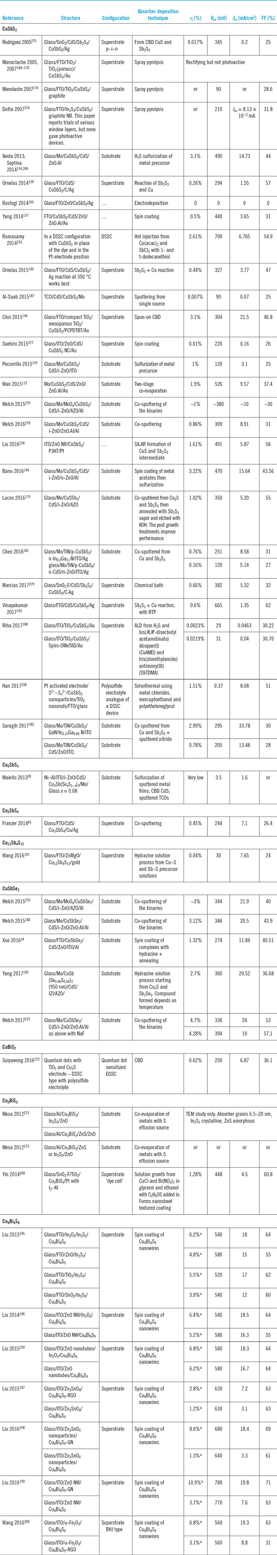
BHJ—bulk heterojunction.
CBD—chemical bath deposition.
GN—graphene nanosheets.
RGO—reduced graphene oxide.
SILAR—successive ionic layer adsorption and reaction.
a Not verified by a test facility or another group—see text.
Overall conclusion on prospects for PVs
Seven materials in the family of Cu–(Sb, Bi)–chalcogenides have band gaps in the range 1–1.5 eV making them potential candidates for the absorber materials in solar PV devices. These are as follows: CuSbS2, Cu3SbS3, Cu3SbS4, Cu3SbSe2, Cu3SbSe3, Cu3BiS3, and Cu4Bi4S9. They comprise elements that are sufficiently Earth abundant for them to be able to make a viable contribution to the future mass market needs for PV devices. The present day thin-film leaders CdTe and CIGS will struggle to fulfill this need due to the scarcity of tellurium and the cost of indium. However, of these materials, only CuSbS2 and CuSbSe2 have demonstrated credible PCEs of >3%, and none have exceeded 5%. The principal device constraint is the low generation of photocurrent. Section “Conclusions and research recommendations for solar PV devices from the Cu-Sb- and Cu-Bi-chalcogenides” of this review offers clear pointers toward missing knowledge that could help resolve this issue: the field is quite immature at this stage, and a significant step change in understanding will be required in order for the Cu–(Sb,Bi)–chalcogenides to realize their potential contribution to large scale PV power generation.
Acknowledgments
EP is grateful to the University of Liverpool for support. The work was also supported by EPSRC Grant Nos. EP/F029624/2 and EP/J017361/1. The authors are indebted to Dr. Ian Forbes Prof David Lane, Dr. Jon Major, Prof Laurie Peter, and Mr. Peter Yates for stimulating conversations in addition to those with the many presenters on the topic at international conferences. We would also like to thank the authors whose work is reproduced here and their publishers for permission to reuse the figures.
Appendix 1: Silver analogues of the Cu–Sb and Cu–Bi chalcogenides
Table A1. Reports of the silver containing compounds as electronic materials and also a list of the known mineralogical phases reported by Moelo.Reference Moelo, Makovicky, Mozgova, Jambor, Cook, Pring, Paar, Nickel, Graeser, Karup-Moller, Balic-Zunic, Mumme, Vurro, Topa, Bindi, Bente and Shimizu7
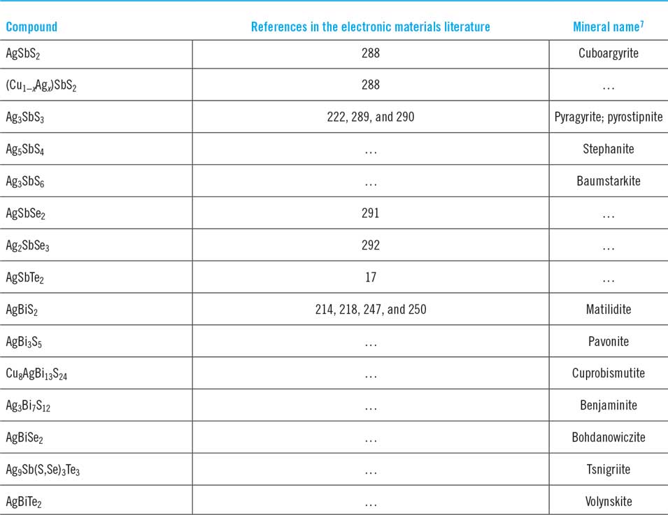


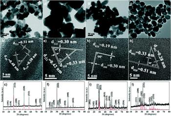


 Open access