
1.1 Introduction
Sources of power in the radiofrequency, microwave, and millimetre wave regions of the electromagnetic spectrum are essential components in a wide range of systems for telecommunications, broadcasting, remote sensing, and processing of materialsFootnote 1. Current research is extending the frequency range into the sub-millimetre region. These sources employ either vacuum electronic, or solid state, technologies. At the higher frequencies and power levels, vacuum electronic devices (tubesFootnote 2) are the only sources available (see Section 1.2).
The purpose of this book is to provide a comprehensive introduction to the theory and conceptual design of the types of tubes which are of continuing importance. The design and operation of vacuum tubes requires knowledge and skills drawn both from electrical and electronic engineering and from physics. The treatment here is intended to be accessible to those whose training has been in either discipline. The use of advanced mathematics has been avoided as far as possible with considerable emphasis on the use of simple numerical methods. The book is designed to be a reference text for designers and users of vacuum tubes, and a textbook for people who are new to the field.
This is a mature field in which much has been published since its first beginnings in 1904 [Reference Fleming1]. The sources cited here are those which have been used as the basis for the book. They are believed to comprise most of the most important sources in the field and the reader is invited to consult them for further information. References have been included to sources that provide additional information on many of the topics, but no attempt has been made to provide a comprehensive bibliography of the subject and longer lists of references are to be found elsewhere [Reference Barker2]. A further aim of this book is to provide the reader with the background necessary to read with understanding other papers in the field.
In any book it is necessary to make choices about what should be included and what excluded. The subjects covered are those the author believes to be important for the practical business of designing and using vacuum tubes. Because the focus is on theory and conceptual design very little has been said about the technology of tube construction, which is well treated elsewhere [Reference Kohl3, Reference Rosebury4]. Similarly, little has been said specifically about vacuum tubes for use at sub-millimetre wavelengths since they employ the same principles as those at lower frequencies, and most of the challenges are in the technology of their construction.
This chapter provides an overview of the subject of the book. The next section compares vacuum tubes with solid-state devices to show how the technologies are complementary. Section 1.3 provides an overview of the physical principles on which vacuum tubes are based and definitions of the key terms used to describe their performance. A tube converts the DC power in the initial electron stream into RF output power by interaction with electromagnetic structures. These structures support standing (resonant), or travelling, electromagnetic waves. Coupled-mode theory is introduced as a valuable conceptual tool for understanding the interactions between electron streams and travelling electromagnetic waves. The section concludes with a classification of the principal types of vacuum tube based on the preceding discussion. The principal applications of vacuum tubes are reviewed in Section 1.4 together with some of the factors which govern the availability of tubes of different types. That leads, in Section 1.5 to consideration of the communication between the designers and users of tubes in the form of a Statement of Requirements. This statement specifies both the electrical performance required, and the factors which constrain the design. Many tubes are required to amplify modulated carrier signals whose properties are not normally familiar to people whose primary discipline is Physics. An introduction to analogue and digital modulation, noise and multiplexing is provided in Section 1.6. Finally, Section 1.7 considers some of the principles of the engineering design of tubes including dimensional analysis and scaling, and the use of computer modelling.
The remainder of the book comprises four sections:
i) Chapters 2–4 deal with the properties of the passive electromagnetic components employed in vacuum tubes.
ii) Chapters 5–11 are concerned with aspects of electron dynamics in vacuum that are employed in tubes in a variety of ways. Chapter 10 also includes a discussion of methods of cooling.
iii) Chapters 12–17 show how the fundamental principles introduced earlier in the book are applied to specific types of tube, and their conceptual design.
iv) Chapters 18–20 provide an introduction to some technological issues which are common to most types of tube and their successful use in systems.
1.2 Vacuum Electronic and Solid-State Technologies
The characteristic size of any active RF device is determined by the distance travelled by the charge carriers in one RF cycle. Thus the size of a device decreases as the frequency increases and as the velocity of the charge carriers decreases. The application of any electronic technology is limited, ultimately, by temperature since the operation of a device generates heat. Hence, the maximum continuous, or average, RF power which can be generated by a single device is determined by the power dissipation within it. At low power levels semiconductor devices have the advantages of small size, and low voltage operation. But these become disadvantages at high power levels because the current passing through the device is high. Thus there are large conduction losses, generating heat, within a small volume. They can be reduced, to some extent, by operating the device as a switch rather than in its active mode.
Transistors can currently deliver around 100 W of continuous power or 1 kW of pulsed power at frequencies in the region of 1 GHz [Reference Trew5–Reference Pengelly7]. Further developments, including transistors using diamond as a semiconducting material, may increase the power to several kW [Reference Kasu8, Reference Camarchia9]. High power amplifiers can be made by operating many transistors in parallel but the penalties of increased complexity set limits to this. The power combining can take place in space, as in active phased-array radar, where average powers up to tens of kilowatts can be achieved [Reference Richards10]. Alternatively, a power combining network may be used as in the 190 kW, 352 MHz, amplifier at Synchrotron SOLEIL [Reference Marchand11]. This amplifier combines the power from four 50 kW towers each containing twenty 2.5 kW units. A unit comprises eight 315 W modules each having a pair of transistors operated in push-pull. This arrangement means that the loss of power from the failure of an individual transistor is small, and the degradation of the amplifier from this cause is gradual. However, the power output is still almost an order of magnitude less than that achieved by vacuum tubes at the same frequency, and the frequency is at the lower end of the range for which vacuum tubes have been developed. The use of low DC voltages reduces problems of reliability caused by voltage breakdown. But the consequent need for high currents leads to DC losses in the connecting bus-bars. A review of high power semiconductor RF power technology is given in [Reference Caverly12].
Vacuum tubes, in contrast, operate at high voltages and low currents. The charge carriers have a much higher velocity than in a semiconducting material, and they are not subject to energy loss through collisions as they pass through it. Thus the active volume can be large with only RF losses within it. In many cases, the greater part of the heat generated is dissipated on electrodes which are separate from the active region, and whose size can be increased to reduce the power density. There is a common misconception that vacuum tubes are fragile, short-lived, unreliable, and inefficient. In fact, modern vacuum devices are mechanically robust and able to survive short-term electrical overloads without damage. They have demonstrated outstanding reliability and lifetimes in the very demanding environment of space. Vacuum tube amplifiers can have maximum conversion efficiencies of up to 70%, and 90% has been achieved in oscillators. However, the most reliable performance of any technology is achieved by allowing generous design margins and operating well within their limits. Vacuum tubes can be operated in parallel, in the same way as semiconductor devices, but the number of parallel devices is usually quite small [Reference Kindermann13, Reference Jensen14]. An exception to this is in phased-array radar where the output from a larger number of microwave power modules (see Section 20.1) is combined in space [Reference Booske and Barker15].
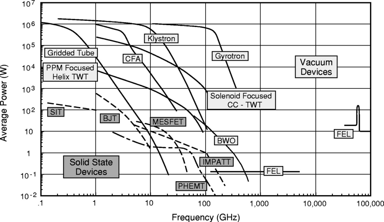
Figure 1.1 shows a comparison between the performances of individual vacuum and semiconductor RF power devices [Reference Granatstein16]. There have been advances in both technologies since that figure was drawn, but the general picture remains valid. A more recent, but less detailed, figure is to be found in [Reference Faillon, Eichmeier and Thumm17]. For further discussion of the relative merits of vacuum tube and solid-state RF power amplifiers see [Reference Booske, Barker and Barker18, Reference Ayllon19]

Figure 1.1: Comparison of the performance of single vacuum electronic and solid state RF power devices.
1.3 Principles of Operation
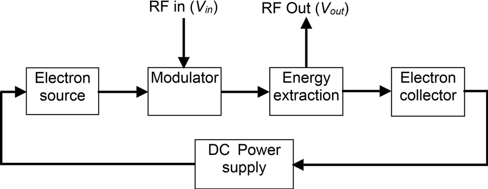
The tubes which are the subject of this book are all power amplifiers and oscillators. For our present purpose it is sufficient to regard oscillators as amplifiers in which the RF input is provided by internal feedback. All vacuum tube amplifiers can be understood in terms of the block diagram shown in Figure 1.2. A uniform stream of electrons is emitted into the vacuum from the electron source and modulated by the RF input voltageFootnote 3. Radiofrequency energy is extracted from the modulated stream of electrons, and their remaining energy is dissipated as heat on a collecting electrode. The arrows show the direction of motion of the electrons; the conventional current is, of course, in the opposite direction. The functions of the blocks may be combined in various ways in different devices but the overall process is essentially the same. The basic RF performance of an amplifier is defined in terms of its gain, output power, efficiency, and instantaneous or tuneable bandwidth.

Figure 1.2: Block diagram of a vacuum tube amplifier.
1.3.1 Geometry
The majority of practical vacuum tubes have geometries which are cylindrically symmetrical, or close approximations to it. The flow of the DC current is radial or axial, and driven by a static electric field in the same direction (see Chapters 5, 8, and 9).
1.3.2 Electron Dynamics
The voltages employed in vacuum tubes are high enough, in many cases, for the velocities of the electrons to be at least mildly relativistic. The kinetic energy of a relativistic electron is [Reference Rosser20]:
 (1.1)
(1.1)
where  is the rest energy of the electron and the relativistic mass is
 (1.2)
(1.2)where u is the velocity of the electron and c the velocity of light. If an electron starts from rest at the cathode then its velocity at a point where the potential is V, relative to the cathode,Footnote 4 is found by using the principle of conservation of energy:
 (1.3)
(1.3)This equation can be rearranged as
 (1.4)
(1.4)
where  is the rest energy of the electron expressed in electron volts. When
  the fraction can be expanded by the Binomial Theorem to give the approximate expression:
 (1.5)
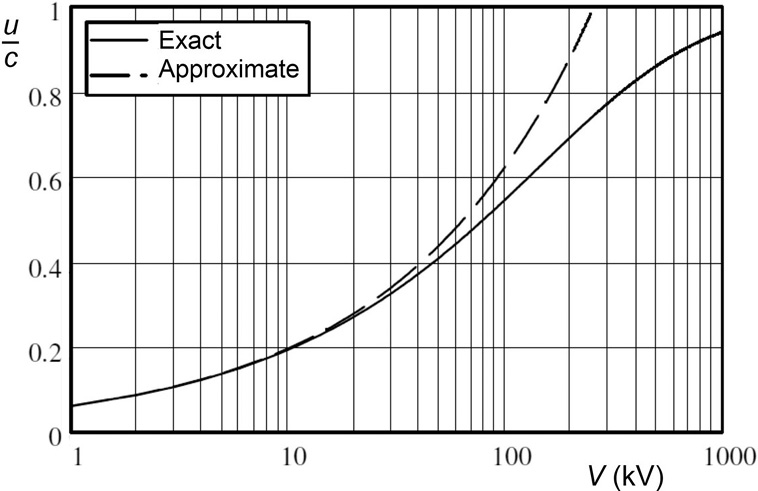
(1.5)Figure 1.3 shows a comparison between the velocities calculated using the exact and approximate equations. The error in the approximate velocity is 1% at 7 kV so that the exact formula should be used for voltages higher than this.

Figure 1.3: Comparison between exact and approximate electron velocities as a function of the accelerating potential.
The force acting on an electron is equal to the rate of change of momentum
 (1.6)
(1.6)If the force acts in the direction of the motion of the electrons then
 (1.7)
(1.7)
where a is the acceleration and  is sometimes called the longitudinal mass. When the force acts at right angles to the direction of motion then
 (1.8)
(1.8)
where  is the transverse mass. If the longitudinal velocity is approximately constant and much greater than the transverse velocity then it is possible to use the classical equations of motion with relativistic corrections to the mass of the electron.
The DC electron current in a tube may be collimated by a magnetic field which is either parallel to the direction of the DC current or perpendicular to it (see Chapters 7 and 8). Tubes in which the field is parallel to the current are described as ‘Type O’ and those in which it is perpendicular as ‘Type M’. The current may also be collimated by a static electric field but this is rather rare.
1.3.3 Modulation of the Electron Current
For the present we will assume that the input RF voltage is purely sinusoidal with amplitude  and frequency
  . Practical input signals are discussed in Section 1.6. It can be shown that the three possible methods of modulation of the current by the RF input voltage are [Reference Gabor21]:
Emission density modulation in which the current emitted from the source is varied.
Deflection and concentration modulation in which the electrons are deflected sideways.
Transit-time modulation in which the electron velocity is varied.
The effect of any of these methods of modulation, or combinations of them, is to produce a bunched stream of electrons whose current varies with time at the frequency of the input signal. Because the process is non-linear the time variation of the current is not sinusoidal but can be represented by a Fourier series. The amplitudes and phases of the harmonic components depend upon the amplitude of the input voltage, and on the distance from the source. The modulation may be either in the same direction as the DC current flow, or normal to it. Thus the current at some point  can be written
 (1.9)
(1.9)
where  is the current in the unmodulated stream,
  are complex amplitudes, and modulation in the axial direction has been assumed. The DC and time-varying parts of the current may be in different directions in space. We note that the real current cannot be negative. Its maximum value, relative to
  , is determined by the process of modulation, or by the maximum current which can be drawn from the source. The ratio I0/I0 cannot exceed 2.0 (see sections 11.8.4 and 13.3.4).
1.3.4 Amplification, Gain, and Linearity
The RF output voltage is obtained by passing the modulated stream through a region at an effective position  where energy is removed from the electron bunches by an RF electric field. This can be represented by an impedance
  which depends on frequency and on the magnitude of the input signal. Thus the output voltage is
 (1.10)
where, for simplicity we assume that the characteristic impedances of the input and output waveguides are the same. The impedance  is effectively zero above some value of the harmonic number n determined by the nature of the output section. Thus the number of harmonics at which there is appreciable output power is small and, in some cases, limited to the fundamental. If the output power is to be radiated it may be necessary to filter out the harmonics to comply with the regulations determining the bandwidth available to the system, as specified by international agreement and national regulations [22, 23]. The transfer characteristic of the amplifier at the frequency
  is then
 (1.11)
where  is the AM/AM (amplitude modulation) characteristic which is usually plotted on decibel scales and
  is the AM/PM (phase modulation) characteristic of the amplifier.
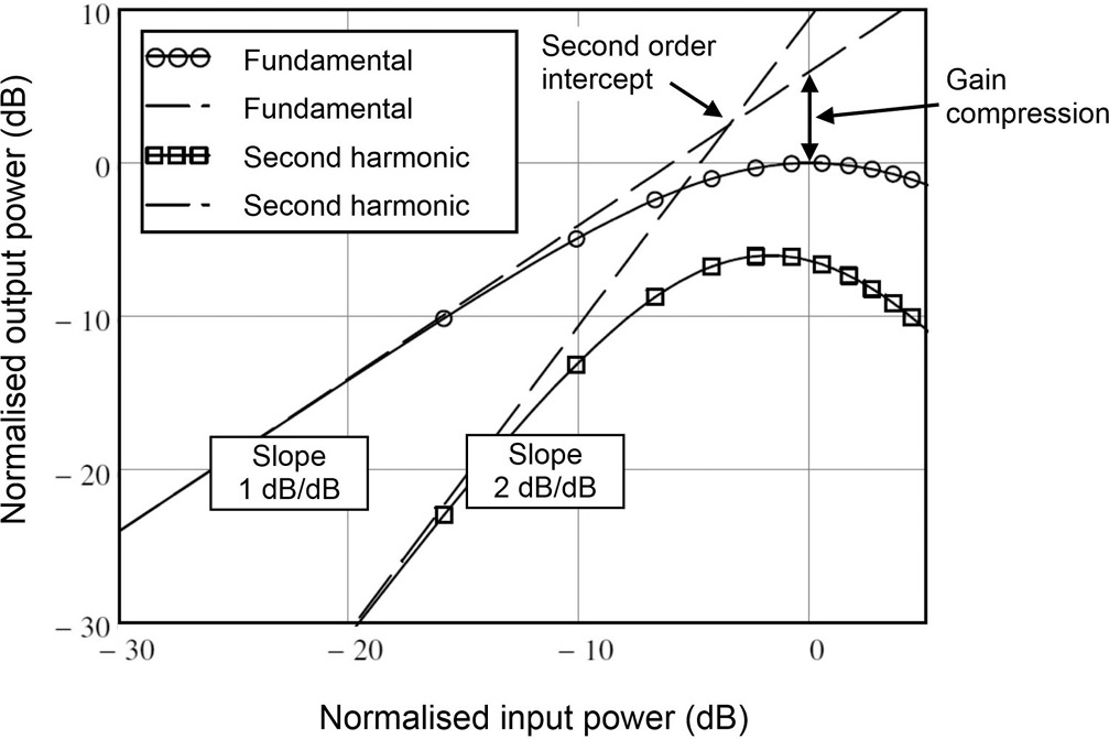
The details of the transfer characteristics depend upon the type of amplifier but many of them show the same features. Figure 1.4 shows, as an example, a typical AM/AM curve of a travelling-wave tube (TWT). The output power is proportional to the input power at low drive levels (slope 1 dB/ dB) but reaches saturation as the input is increased. In the figure the input and output powers have been normalised to their values at saturation. The gain of the amplifier in decibels is given by
 (1.12)
where  and
and  are, respectively, the input and output power. Since we have assumed that the input and output waveguides have the same characteristic impedances we can write
 (1.13)
The difference between the linear (small-signal) and the saturated gain is the gain compression which may be used as a measure of non-linearity. It is common for a tube to be described in terms of its saturated output power, but the output power available under normal operating conditions may be less than this. For example the tubes used in particle accelerators are normally operated ‘backed-off’ from saturation to provide a control margin for the operation of the accelerator. In a TWT there is normally some output at second, and higher, harmonic frequencies. This also depends on the input drive level as shown in Figure 1.4. At low drive levels the second harmonic output is proportional to the square of the input power, giving a slope of 2 dB/dB. The maximum second harmonic power does not necessarily occur at the drive level that saturates the fundamental. The intersection between the projections of the linear parts of the fundamental and second harmonic curves, known as the second-order intercept point, is a measure of the second-order distortion of the amplifier.

Figure 1.4: Typical curves of fundamental and second harmonic output power of an RF amplifier plotted against the input power, normalised to saturation.
The corresponding AM/PM curve for a TWT is shown in Figure 1.5. The phase is plotted relative to the phase at low drive levels, and the input power is normalised to the input power at saturation. The phase of the output signal relative to the input is constant at low drive levels but changes as the drive level is increased. Both the amplitude and phase of the output depend on frequency, and on the operating conditions of the amplifier, including the voltages applied and the external RF matches. Thus any ripple in the voltages applied may result in amplitude and phase modulation of the output signal. In an oscillator, voltage ripple may also produce frequency modulation.
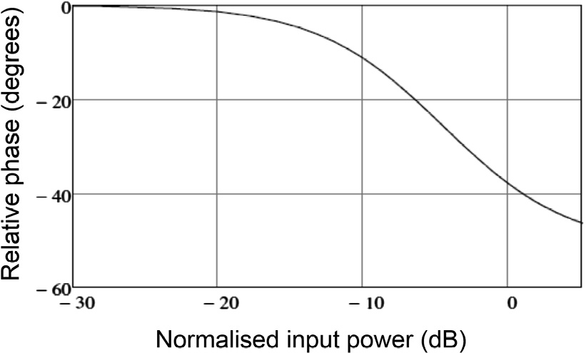
Figure 1.5: Typical curve of the phase of the output voltage of an RF amplifier against input power normalised to saturation.
1.3.5 Power Output and Efficiency
An important consideration for many applications of tubes is the efficiency with which the DC input power is converted into useful RF power. The principle of conservation of energy requires that, in the steady state, the total input and output powers must balance, that is
 (1.14)
The DC input power includes the power in the electron stream, the cathode heater, and electromagnets. If the tube has a depressed collector (see Section 10.3) the DC power is reduced by the power recovered by the collector. When a comparison is made between alternative tube types, or between vacuum tube and solid-state amplifiers, then the DC input power should be specified at the input to the power supply to allow for losses in it. Any power required for cooling fans or pumps must also be included. The RF output power comprises power at the fundamental frequency and its harmonics. Heat is generated by the impact of electrons on the collector and the tube body and by RF losses in the tube body, connecting waveguides and windows.
A number of different definitions of efficiency are in use and it is important to distinguish between them. The overall efficiency is defined here as the ratio of the fundamental RF output power  to the total input power to the tube
 (1.15)
If the gain of the amplifier is high, the RF input power is much smaller than the DC input power so that approximately
 (1.16)
The heater and electromagnet powers are typically much smaller than the stream power in continuous wave (CW) tubes but they can be comparable with the stream power in pulsed tubes. The power added efficiency, sometimes used when the gain is small, is
 (1.17)
This efficiency is effectively identical to that in (1.16) if the gain is 20 dB or more. The efficiency of tubes with depressed collectors is discussed in Section 10.3. The RF efficiency is defined here as the ratio of the useful RF output power to the power input to the electron stream (less any recovered by the collector) plus the RF input power.
 (1.18)
The electronic efficiency is the efficiency with which power is transferred from the electron stream to the RF electric field of the output circuit.
 (1.19)
where  is the total RF power loss in the output circuit. If the output circuit is resonant so that only power at the fundamental frequency is included
 (1.20)
where P2,loss is the RF loss at the fundamental frequency. Then the circuit efficiency can be defined by
 (1.21)
If, in addition, the RF input power is small enough to be neglected, and the tube does not have a depressed collector then the RF efficiency is
 (1.22)
1.3.6 Bandwidth
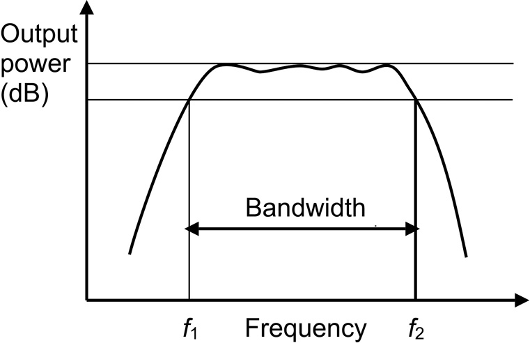
The AM/AM, and AM/PM, curves depend upon the frequency of the input signal. Then the transfer function of the amplifier may be written  . Figure 1.6 shows a typical graph of the RF output power of an amplifier as a function of frequency. This graph may be plotted at constant input power, or showing the saturated output power at each frequency. The bandwidth is defined in terms of the frequencies at which the power falls below the maximum by a specified amount (e.g. 1 dB bandwidth). This may be expressed in absolute terms or as a percentage of the centre frequency. The figure also shows that the output power may vary within the band and this can affect the system in which the tube is employed. These ripples are normally greatest when the tube is not saturated and are reduced at saturation by the effects of gain compression. The custom of using a decibel scale for this graph can be misleading. It is important to remember that a change of −1 dB represents a reduction in power by 20% and a change of −3 dB a reduction of 50%. Similar graphs of efficiency, small-signal gain, and saturated gain against frequency can also be plotted. The bandwidth specified for a tube may be to permit rapid changes in frequency (as in frequency-agile radar), or to enable it to be used with multiple and modulated signals (see Section 1.6).

Figure 1.6: Typical graph of the output power of an RF amplifier plotted against frequency.
In addition to power at harmonics of the input frequency the output of a tube may also include non-harmonic power under some operating conditions (for example during the rise and fall of the pulse during pulsed operation). These out-of-band emissions are undesirable, and limits are usually specified to avoid interference with other systems. For example it has been known for out-of-band emissions from marine radar, and from industrial microwave ovens, to interfere with microwave communication links. The tube also contributes to the noise in the system as discussed in Section 1.6.1.
1.3.7 The Electromagnetic Structure
The electromagnetic structures used to modulate the electron stream, and to extract power from it, can be divided into three groups:
Fast-wave structures in which the phase velocity of travelling waves is greater than the velocity of light (Chapter 2).
Resonant (standing wave) structures in which the RF electric field profile is time-varying but fixed in space (Chapter 3).
Slow-wave structures which employ the field of a travelling electromagnetic wave whose phase velocity is less than the velocity of light (Chapter 4).
The bandwidth of a tube using a resonant structure is typically restricted to a few percent by the loaded  of the resonance (see Section 3.2.2). If the higher-order modes of the structure do not coincide with harmonics of the input frequency then the harmonic output of the tube is small.
The bandwidths of tubes using travelling-wave structures can be broad because the phase velocity and the impedance presented to the electron current by the structure vary slowly with frequency. The interaction is distributed so that the bunching section and the output section of the tube are effectively combined. For useful interaction to take place the mean electron velocity must be approximately synchronous with the phase velocity of the wave. There may be interaction at harmonics of the input frequency leading to appreciable output power at the second and higher harmonics as shown in Figure 1.4.
1.3.8 Coupled-Mode Theory
Useful insights into the properties of travelling-wave structures and their interactions with electron streams under small-signal (linear) conditions are given by coupled-mode theory [Reference Pierce24–Reference Pierce28]. For this purpose the small-signal modulation of the electron stream is described by a pair of normal modes whose impedances have opposite signs. The properties of space-charge waves on electron beams are discussed in detail in Chapter 11.
The properties of a wave propagating as  are the solutions to the dispersion equation
 (1.23)
where the frequency (w) and the propagation constant (β) are real if there is no attenuation.Footnote 5 The solutions of the dispersion equation can be plotted on a dispersion  diagram. In this diagram the phase velocity of the wave is
 (1.24)
and the group velocity, which is taken to be the velocity of propagation of energy, is
 (1.25)
The phase velocity is positive in the first quadrant of the  diagram and negative in the second quadrant. The group velocity can be either positive or negative depending upon the properties of the mode. We shall see in Chapter 4 that waves having positive phase velocities and negative group velocities occur in periodic structures.
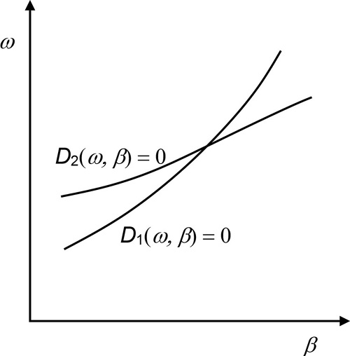
Where two waves propagate in the same region of space they may interact to produce coupled modes if their dispersion curves intersect as shown in Figure 1.7. The dispersion equation for the coupled modes can then be written in the form
 (1.26)
where  represents the coupling between the modes. The coupled modes are the solutions to this equation. In order to investigate the properties of coupling under different conditions we will redefine
  and
and  so that the two uncoupled modes intersect at the origin. This transformation does not change the group velocities of the modes.

Figure 1.7: Dispersion diagram for two modes of propagation.
The properties of the different possible kinds of mode coupling can be illustrated by assuming that the uncoupled dispersion curves are straight lines so that
 (1.27)
The dispersion equation for the coupled modes is then
 (1.28)
where  is regarded as a constant close to the origin. This equation can be expanded to give
 (1.29)
which is quadratic in both  and
and  . Solving for
  gives
gives
 (1.30)
and for  gives
gives
 (1.31)
The constant  is positive if the signs of the impedances of the uncoupled waves are the same, and negative if they are opposite. Likewise the signs of the group velocities of the waves may be the same, or opposite. Hence all possible combinations are covered by four cases, which can be explored using Worksheet 1.1. It can be shown that the properties of the coupled modes can be revealed by considering the solutions of (1.30) when
  is real and the solutions of (1.31) when
  is real as follows [Reference Briggs26, Reference Sudan29]:
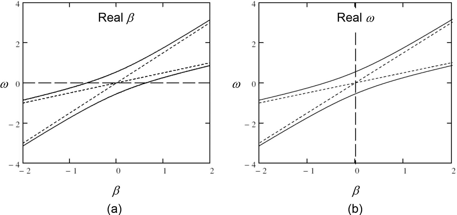
Case A: The group velocities and the impedances have the same sign  .
.
When  is real the solutions of (1.30) are always two real values of
  and, when
  is real, the solutions of (1.31) are two real values of
  . These solutions represent travelling waves with the modified dispersion diagram shown in Figure 1.8. In Figures 1.8 to 1.11 the uncoupled modes are shown by dotted lines, the real parts of the solutions by solid lines and the imaginary parts by dashed lines.

Figure 1.8: Coupling between two forward waves with impedances having the same sign: (a)  for real
  , and (b)
  for real
  .
.
Case B: The group velocities have opposite signs and the impedances have the same sign  .
.
When  is real the solutions of (1.30) are always two real values of
  but, when
  is real and close to the origin, the solutions of (1.31) are complex conjugate pairs of values of
  , as shown in Figure 1.9(b). Physically, the complex values of
  represent travelling waves whose amplitudes decay exponentially with distance. For example see Figure 4.28(a) where the forward and backward waves in a waveguide are coupled to one another by periodic discontinuities to produce frequency stop-bands in which there are decaying (evanescent) waves.
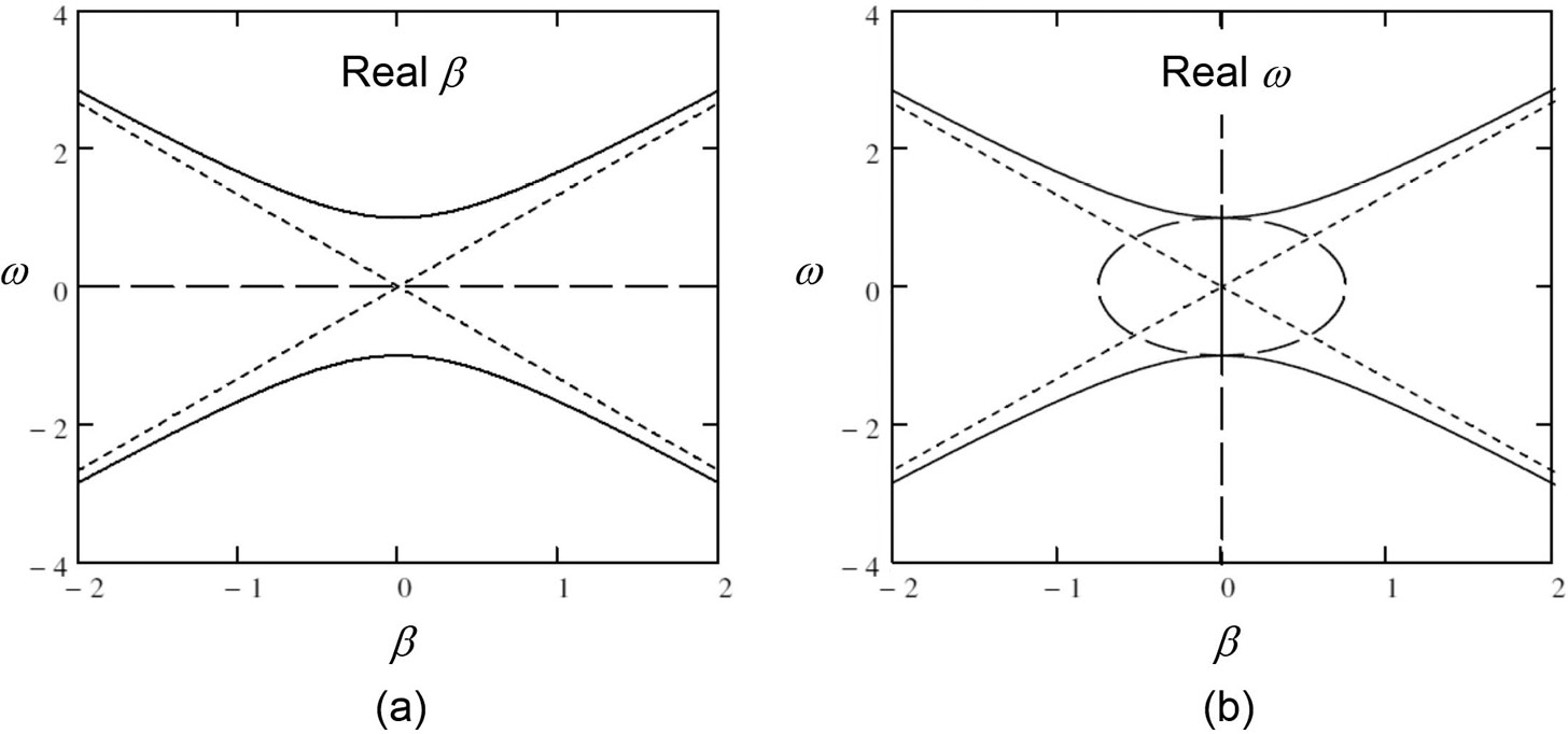
Figure 1.9: Coupling between a forward wave and a backward wave with impedances having the same sign: (a)  for real
  , and (b)
  for real
  .
.
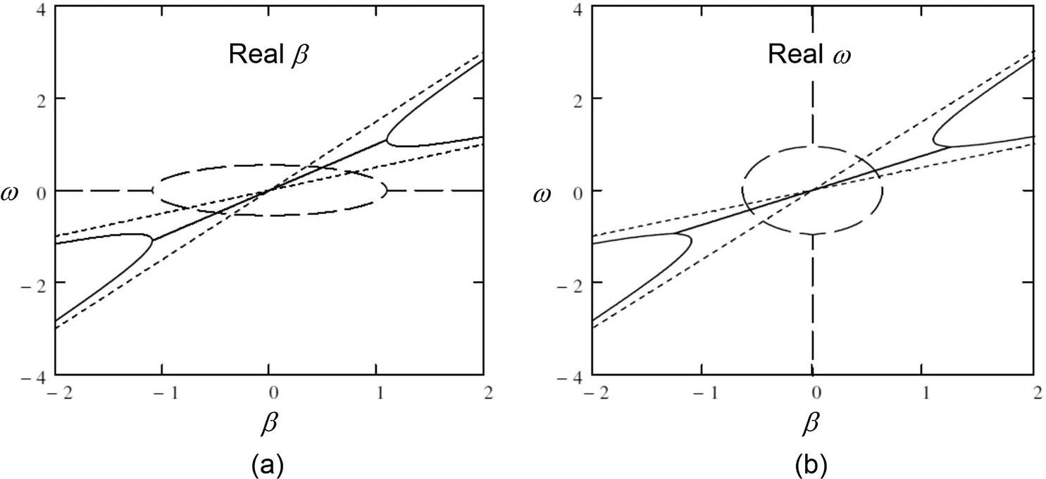
Case C: The group velocities have the same sign and the impedances have opposite signs 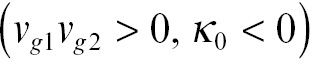 .
.
The solutions for both  and
and  , close to the origin, are complex conjugate pairs, as shown in Figure 1.10. It can be shown that the complex solution for
  corresponds to a convective instability in which the waves grow and decay exponentially in space (see Figure 1.10(b)) [Reference Briggs26, Reference Sudan29]. An example of this type of coupling is the growth of waves in a travelling-wave tube as shown in Figure 11.19.

Figure 1.10: Coupling between two forward waves with impedances having opposite signs: (a)  for real
  , and (b)
  for real
  .
.
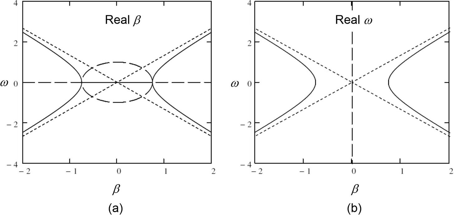
Case D: The group velocities and the impedances have opposite signs 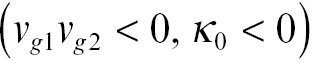 .
.
When  is real and close to the origin the solutions of (1.30) are a complex conjugate pair of values of
  and, when
  is real, the solutions of (1.31) are always two real values of
  , as shown in Figure 1.11. The solution with complex
  is a non-convective, or absolute, instability in which the two solutions grow and decay exponentially in time. The condition for this instability to exist is that there is at least one value
  in the upper half of the complex plane for which there are coincident roots in
  [Reference Sudan29]. For the case considered here the condition for the existence of coincident roots is found from (1.31)
 (1.32)
The condition is satisfied in this case when  and
and  so that an absolute instability exists for all negative values of
  . The corresponding values of
  can be found from (1.31):
 (1.33)
Thus  is complex when
  is complex. In general the start-oscillation condition can be found by finding the least magnitude of the coupling for which coincident roots of
  exist when
  is real (see Figures 17.5 and 17.6) [Reference Chu and Lin30]. If the coupling is increased beyond this point both the frequency and the propagation constant are complex (see Section 11.7). Examples of this kind of instability are backward-wave oscillations in a travelling-wave tube (Section 11.7) and gyrotron oscillators (Section 17.3).

Figure 1.11: Coupling between forward and backward waves with impedances having opposite signs: (a)  for real
  , and (b)
  for real
  .
.
The properties of coupled modes remain the same in more general cases where the uncoupled dispersion diagrams are not straight lines,  is a function of
  and
and  , and more than two modes are involved in the coupling. Thus a qualitative description of the properties of the coupled system can be derived from an examination of the dispersion diagram of the uncoupled modes and the form of the dispersion equation for the coupled system [Reference Sudan29].
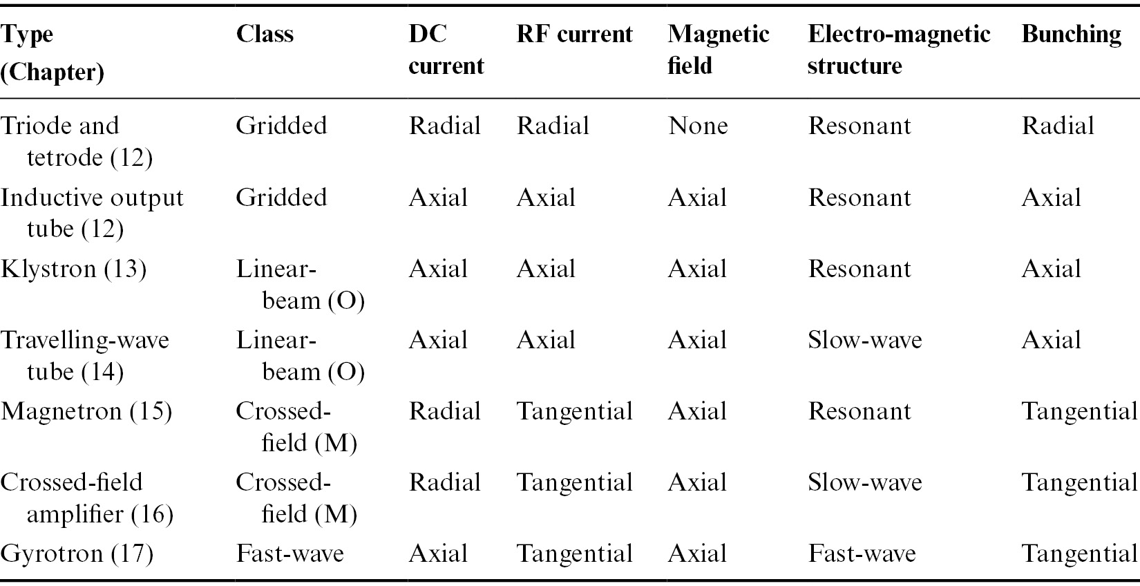
1.3.9 Classification of Vacuum Tubes
The preceding sections have reviewed the different ways in which the functional blocks in Figure 1.2 can be realised, and that can be used as a basis for classifying tubes. The discussion in this book is restricted to the types of tube which are of continuing practical importance. A summary of their principal features is given in Table 1.1. A few variations on the main types of tube exist, for example: triodes and tetrodes with DC and RF current flow in the axial direction, and hybrid tubes in which the bunching section resembles a klystron and the output section a travelling-wave tube. It is possible to think of the inductive output tube as a hybrid tube with a triode bunching section and a klystron output section. Many other possible types of tube can be envisaged [Reference Feinstein and Felch31–Reference Harvey33].
Table 1.1: Classification of the principal types of vacuum tube
1.4 Applications of Vacuum Tubes
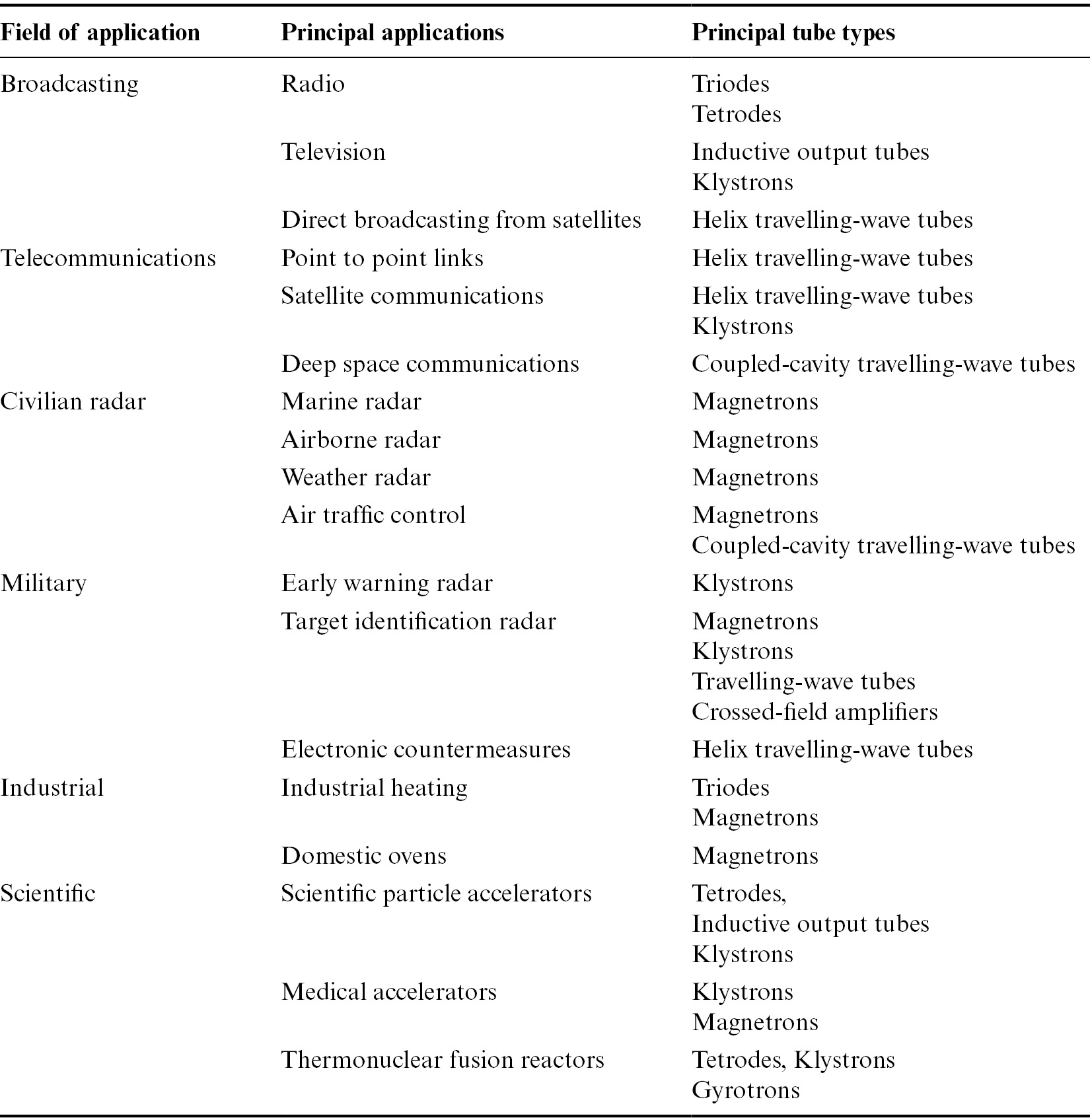
High-power vacuum tubes have found applications in many fields as summarised in Table 1.2 [Reference Faillon, Eichmeier and Thumm17]. A comprehensive summary of the historical development of tubes for the microwave and millimetre-wave region of the spectrum can be found in [Reference Luhmann and Barker34, Reference Granatstein35]. For the history of power gridded tubes and their applications see [Reference Yingst36].
Table 1.2: The principal applications of vacuum tubes
| Field of application | Principal applications | Principal tube types |
|---|---|---|
| Broadcasting | Radio | Triodes Tetrodes |
| Television | Inductive output tubes Klystrons | |
| Direct broadcasting from satellites | Helix travelling-wave tubes | |
| Telecommunications | Point to point links | Helix travelling-wave tubes |
| Satellite communications | Helix travelling-wave tubes Klystrons | |
| Deep space communications | Coupled-cavity travelling-wave tubes | |
| Civilian radar | Marine radar | Magnetrons |
| Airborne radar | Magnetrons | |
| Weather radar | Magnetrons | |
| Air traffic control | Magnetrons Coupled-cavity travelling-wave tubes | |
| Military | Early warning radar | Klystrons |
| Target identification radar | Magnetrons Klystrons Travelling-wave tubes Crossed-field amplifiers | |
| Electronic countermeasures | Helix travelling-wave tubes | |
| Industrial | Industrial heating | Triodes Magnetrons |
| Domestic ovens | Magnetrons | |
| Scientific | Scientific particle accelerators | Tetrodes, Inductive output tubes Klystrons |
| Medical accelerators | Klystrons Magnetrons | |
| Thermonuclear fusion reactors | Tetrodes, Klystrons Gyrotrons |
In general, the development of high power vacuum tubes has been driven by the requirements of particular applications. The number of tubes of each type needed has not been great enough to allow the use of high volume manufacturing methods. The exception to this rule is the domestic microwave oven magnetron where very large numbers have been made. The cost per tube is then dramatically reduced when compared with magnetrons of other types. In some cases tubes, which have been developed for one purpose, have found applications elsewhere. For example high power tetrodes for radio transmitters and klystrons for television and radar transmitters have been used in particle accelerators. However, if the primary market declines, the manufacturers may not continue to produce tubes for low-volume secondary applications. This was a major motivation for the development of high power solid state amplifiers for the SOLEIL synchrotron [Reference Marchand11]. Thus the nature of the market for high power vacuum tubes dictates the need for close communication between the engineers developing a tube and those working on the system in which it will be used. This pattern, which is typical of other markets for low-volume, high-technology, products is quite different from that for high-volume products. The successful incorporation of complex components, such as tubes, into a system requires the systems engineers to have a detailed understanding of how they work. It is not sufficient to regard tubes as ‘black boxes’ whose performance can be described completely by characteristics defined at their terminals. Tube engineers must, likewise, have a detailed understanding of the issues which are important for the systems in which their products are used. Some of these are reviewed in this chapter and in Chapter 20. For further information see [Reference Sivan37].
1.5 The Statement of Requirements
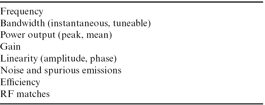
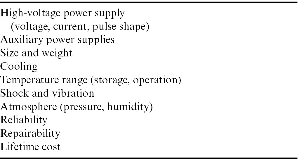
A fundamental document for communication between the customers and the contractors for any engineering product is the Statement of Requirements (also known as a Requirements Specification or a Statement of Work). It is the source from which two further documents are derived: the Manufacturing Specification (or Manufacturing Data Package), which provides all the information required to manufacture the product; and the Test Specification, which gives details of the tests that the product must undergo to demonstrate its compliance with the requirements. It is self-evident that any omissions or ambiguities in these documents will potentially lead to failure to achieve the outcome desired. Thus it is essential that the Statement of Requirements and the Test Specification are produced by an open dialogue between representatives of the customer and the contractor, both of whom fully understand the issues involved. For this purpose it is helpful to have a checklist of the issues to be discussed [Reference Sivan37, 38]. These issues fall into two main groups: the performance requirements; and the design constraints. Typical top-level requirements are shown in Tables 1.3 and 1.4. The following sections discuss some of the issues which are important in the specification of performance requirements.
Table 1.3: Typical performance requirements for vacuum tube amplifiers
| Frequency Bandwidth (instantaneous, tuneable) Power output (peak, mean) Gain Linearity (amplitude, phase) Noise and spurious emissions Efficiency RF matches |
1.6 Signals and Noise
In order to transmit information for telecommunications (one to one) or broadcasting (one to many) it is necessary for the properties of the sinusoidal carrier wave to be modulated by varying them with time. The properties of the input signal which may be varied are amplitude, phase, and frequency. Many different methods of modulation are in use and only a brief summary is given here of the factors that are important in the specification of vacuum tube amplifiers [Reference Dunlop and Smith39–Reference Anderson41]. The methods fall into two classes: analogue modulation in which the properties of the carrier vary continuously with time; and digital modulation in which they are switched between a number of states.
The baseband input signal is typically defined as a time-varying voltage. This could represent a continuously varying, analogue, source such as a speech or music waveform. Alternatively it could represent a digital source such as a computer data file, or the digitised form of an analogue waveform. It is common, for convenience of analysis, to assume that the input signal is random when observed over an extended period of time, though this is frequently not the case. The frequency spectrum of the signal is obtained by taking the Fourier transform of the waveform. Theoretically this spectrum extends to infinity but, in practice, it is assumed to be restricted to a bandwidth that extends from DC up to some maximum frequency. The upper limit may be somewhat arbitrary and be defined as the point at which the power density in the spectrum falls below a certain limit. This still applies if the bandwidth of the signal has been limited by a filter, since no practical filter has an infinitely sharp cut-off.
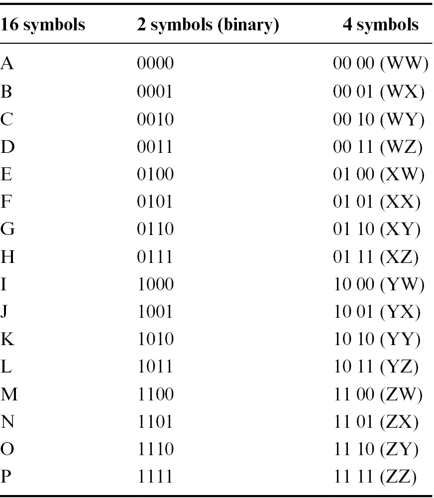
The basic digital signal is binary in which the voltage switches between two states at a fixed clock rate. However, it is often useful to convert this into a form in which a greater number of states is employed. This can be illustrated by considering Table 1.5, which shows different possible representations of the symbols in a sixteen character set.
Table 1.5: Representation of digital signals
| 16 symbols | 2 symbols (binary) | 4 symbols |
|---|---|---|
| A | 0000 | 00 00 (WW) |
| B | 0001 | 00 01 (WX) |
| C | 0010 | 00 10 (WY) |
| D | 0011 | 00 11 (WZ) |
| E | 0100 | 01 00 (XW) |
| F | 0101 | 01 01 (XX) |
| G | 0110 | 01 10 (XY) |
| H | 0111 | 01 11 (XZ) |
| I | 1000 | 10 00 (YW) |
| J | 1001 | 10 01 (YX) |
| K | 1010 | 10 10 (YY) |
| L | 1011 | 10 11 (YZ) |
| M | 1100 | 11 00 (ZW) |
| N | 1101 | 11 01 (ZX) |
| O | 1110 | 11 10 (ZY) |
| P | 1111 | 11 11 (ZZ) |
Let us suppose that we wish to transmit a message made up of the 16 characters in the first column at a rate of 1 symbol/sec. It is helpful to think of these characters as representing 16 different voltage levels in a stepwise approximation to an analogue waveform. A little thought shows that the highest frequency is obtained when any pair of symbols is repeated alternately (e.g. ABABABA). The Fourier transform of all other sequences has a lower maximum frequency.
If we now wish to transmit the same information in binary form we must send four binary digits (bits) per second. The highest frequency is obtained when the symbols 0 and 1 are repeated alternately (e.g. FFFF, or KKKK). Finally we can represent the 16 symbols by a four-symbol set by grouping the binary digits in pairs as shown in the third column. Now the highest frequency is obtained when any pair of symbols is repeated alternately (e.g. WXWX = BB). From this it can be seen that the bandwidth required to transmit the same message depends upon the number of symbols in the set used to represent it. Alternatively, we see that the maximum data rate for a fixed bandwidth is increased by a factor of two if a four-symbol set is used, and by a factor of four with a 16-character set. Now an ideal low-pass channel of bandwidth B can transmit  pulses per second. Thus the maximum rate at which data can be transmitted over this channel is given by Hartley’s law
 (1.34)
where m is the number of symbols used.
1.6.1 Noise
Any communications system adds white noise to the input signal so that the signal received is corrupted to some extent [Reference Dunlop and Smith39]. The thermal noise power in watts caused by the random motion of charge carriers in resistive materials that is delivered to a matched load is
 (1.35)
where k is Boltzmann’s constant  , T is the absolute temperature and
  is the bandwidth of the system in Hz. The effectiveness of an analogue communication system is measured by the signal to noise ratio
  where
where  is the average signal power. This is commonly expressed in decibels as
 (1.36)
The minimum acceptable SNR for reliable communication is generally taken to be about 10 dB.
For digital communications the corruption of the signal may result in some of the bits being received incorrectly. Shannon’s theorem states that a noisy channel will theoretically support error-free data transmission at a channel capacity given by
 (1.37)
This can be expressed alternatively as
 (1.38)
where  is the energy per bit,
  is the mean bit rate, and
  is the spectral energy density of the noise. Shannon’s law represents an ideal which cannot be achieved in practice, but it remains useful for comparison with practical systems. In a digital transmission system the energy per bit, which is related to the bit error rate, is commonly used in place of the signal to noise ratio [Reference Ziemer and Meyers40]. A second performance measure is the bandwidth efficiency
  in bits s−1 Hz−1.
Each part of a communications channel contributes some noise to the system. Here we are concerned specifically with the contribution from the final power amplifier. The noise generated by an amplifier can be described by its noise figure, which is the ratio of the signal to noise ratio at the input to that at the output
 (1.39)
If an amplifier has a power gain  then the signal to noise ratio at the output is
 (1.40)
where  and
and  are the signal and noise powers at the input and
  is the noise power added by the amplifier. Thus
 (1.41)
The noise figure is standardised by fixing the input noise power as that given by (1.35) when  The noise added by the amplifier can be described by an equivalent noise source at its input such that
 (1.42)
where  is the effective noise temperature of the amplifier. The noise performance can also be described by the total noise power at the output, or by the noise power density (noise power per Hz).
1.6.2 Analogue Modulation
In order to transmit the baseband signal over a wireless channel it must be superimposed upon an RF carrier wave by a modulator. The properties of the carrier wave which can be varied by the modulator are its amplitude, frequency, and phase, or some combination of them. In general the modulated signal at the input to the power amplifier can be described by a sinusoidal carrier whose amplitude and phase are functions of time [Reference Berman and Mahle42, Reference Saleh43]. Thus
 (1.43)
where  is the carrier frequency. The rates of change with time of the amplitude
  and phase
  are normally much slower than that of the carrier wave so that it is permissible to regard the instantaneous response of the amplifier as being that for a single unmodulated carrier wave. The response to more complex signals can therefore be deduced from the steady-state, single-carrier, transfer characteristics. Figure 1.12 shows examples of simple analogue modulation schemes. For purposes of illustration the modulation frequency has been taken to be one eighth of the carrier frequency although the ratio is normally much smaller than that.

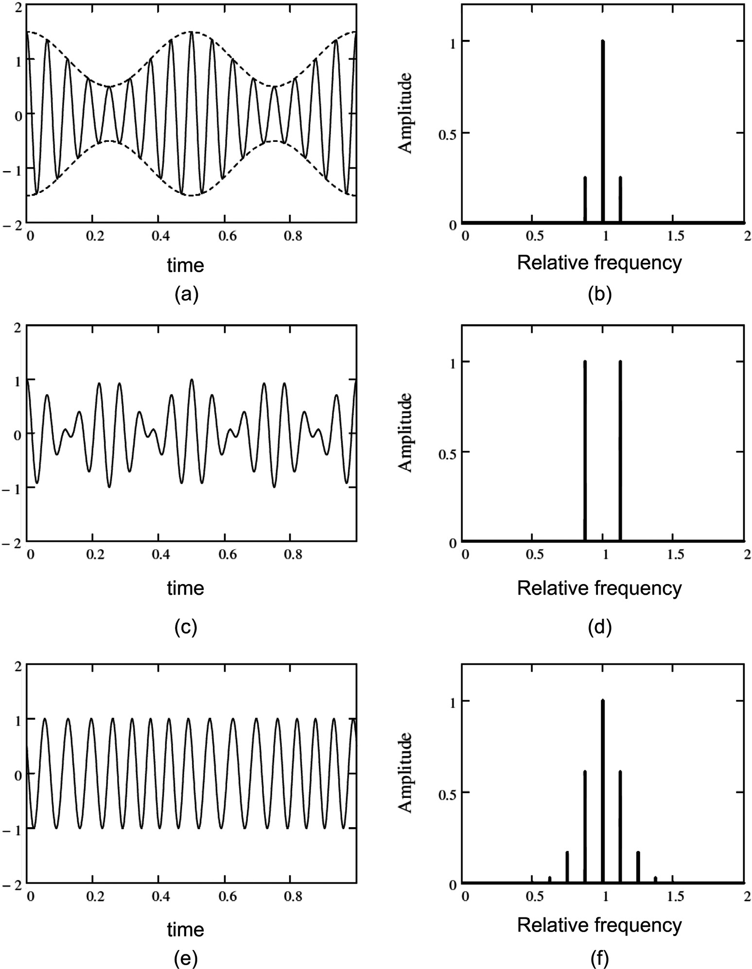
Figure 1.12: Time and frequency domain representations of analogue modulated carriers: (a) and (b) double sideband amplitude modulation; (c) and (d) double sideband suppressed carrier amplitude modulation; (e) and (f) phase modulation.
The simplest example to understand is the amplitude modulation shown in Figure 1.12(a). The envelope of the carrier carries information such as an audio waveform. In the time domain the modulated waveform is given by
 (1.44)
where K is the amplitude of the unmodulated carrier and  is the signal waveform. When the signal is sinusoidal with frequency
  the Fourier transform of
  yields the spectrum in the frequency domain shown in Figure 1.12(b). This representation shows the amplitudes, but not the phases, of the components of the signal. The central line at the carrier frequency is flanked by two sidebands at frequencies
  . This is known as double sideband amplitude modulation. For a more general modulating waveform the sidebands are the frequency-shifted Fourier transforms of the baseband waveform. Faithful transmission of the modulated waveform requires the bandwidth of the amplifier to be at least
  (the Nyquist limit) where B is the baseband bandwidth. The instantaneous power in the modulated signal varies with time, as can be seen from Figure 1.12(a). Faithful transmission of the signal requires the amplifier to be linear up to the highest instantaneous power. Any non-linearity of the amplifier produces a distortion of the signal in the time domain which is reflected in changes in its spectrum (see Section 1.6.4).
Figures 1.12(c) and (d) show double sideband suppressed carrier modulation. The modulated waveform is
 (1.45)
The spectrum differs from that in Figure 1.12(b) in the absence of the carrier frequency. The bandwidth requirements for the amplifier are the same as in the previous case and the dynamic range is greater. However, this modulation scheme is less susceptible to interference from noise than the previous case because all the power is in the sidebands.
Figures 1.12(e) and (f) show phase modulation. The amplitude envelope of the signal is constant in the time domain so that the instantaneous power is constant. This has the advantage that the working point of the amplifier is virtually constant, so that the output signal is only affected by the frequency dependence of the gain and phase of the amplifier. The modulated signal, assuming unity amplitude, is
 (1.46)
so that the dependence of the modulated signal on the modulation is non-linear. For sinusoidal modulation at frequency  (1.46) can be written
 (1.47)
where  is the modulation index. The spectrum for this waveform, shown in Figure 1.12(f) for
  , has additional lines at frequencies
  where
where  . Thus the bandwidth required for faithful amplification is greater than for amplitude modulation schemes. A rule of thumb for the transmission bandwidth is Carson’s rule [Reference Ziemer and Meyers40]
 (1.48)
Frequency modulation can also be represented by (1.47) so that its properties are similar to those of phase modulation. The properties of analogue modulation schemes can be explored using Worksheet 1.2.
1.6.3 Digital Modulation
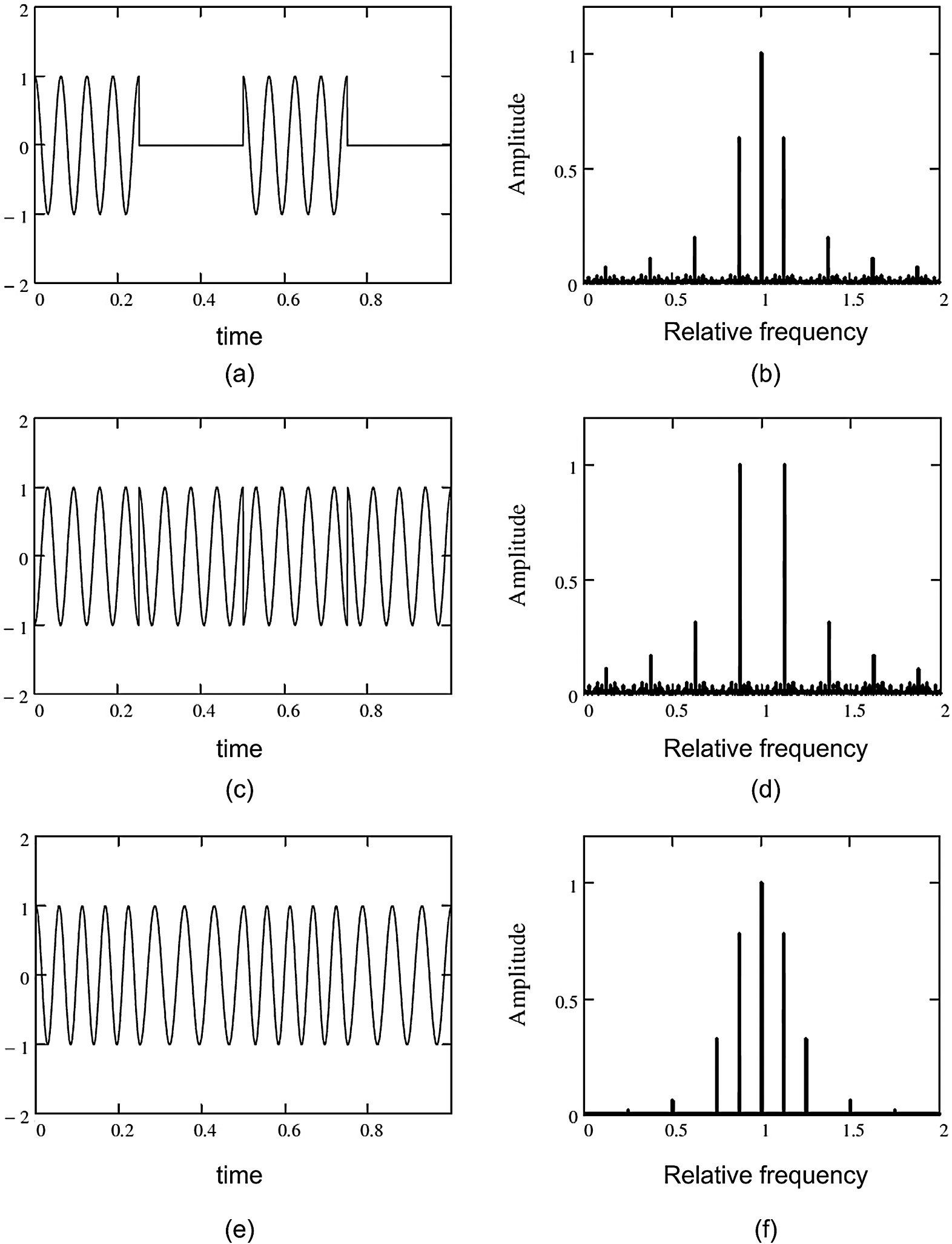
The simplest digital modulation schemes are amplitude shift keyed (ASK), phase shift keyed (PSK), and frequency shift keyed (FSK) modulation [Reference Dunlop and Smith39]. Figure 1.13 shows time and frequency domain representations of these methods of modulation, using the same carrier and modulation frequencies as before. It may be observed that the bandwidths of these signals are greater than those for the equivalent analogue modulation, with the exception of binary FSK modulation, which may be considered a special case of frequency modulation. The properties of binary digital modulation schemes can be explored using Worksheet 1.2.

Figure 1.13: Time and frequency domain representations of simple digitally-modulated carriers: (a) and (b) binary ASK; (c) and (d) binary PSK; (e) and (f) binary FSK.
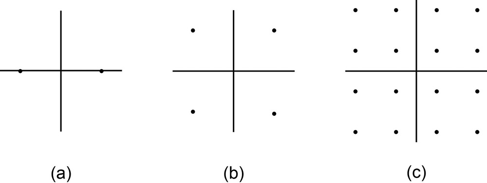
We saw in Section 1.6.1 that the bit rate in a digital system having fixed bandwidth can be increased by using a greater number of symbols. Two common implementations of this principle are illustrated in Figure 1.14 which shows the positions of the symbols on phasor diagrams known as constellation plots. Figure 1.14(a) shows binary phase-shift keyed (BPSK) modulation with a phase shift of 180° corresponding to Figure 1.13(c) and (d). Quadrature phase-shift keyed (QPSK) modulation is shown in Figure 1.14(b), and quadrature amplitude modulation with 16 symbols (16-QAM) is shown in Figure 1.14(c). The effect of noise in the transmission channel is to produce a scatter of points around the desired constellation points at the receiver. If the scatter is too great then the receiver will fail to identify the symbols correctly leading to errors in transmission. Table 1.6 shows the bandwidth efficiencies and  figures for these three channels at a bit error rate of
  . These figures assume coherent modulation so that the clock signals at the transmitter and the receiver are locked to one another. It can be seen that the bandwidth efficiency increases with the number of symbols according to (1.34) as expected.

Figure 1.14: Examples of constellation diagrams for digitally-modulated carriers: (a) binary phase-shift keyed (BPSK), (b) quadrature phase-shift keyed (QPSK), and (c) quadrature amplitude modulation with 16 symbols (16-QAM).
Table 1.6: Comparison between examples of coherent digital modulation schemes [Reference Ziemer and Meyers40]
| Modulation type | Bandwidth efficiency (bits s−1 Hz−1) |  |
|---|---|---|
| BPSK | 0.5 | 10.6 dB |
| QPSK | 1.0 | 10.6 dB |
| 16-QAM | 2.0 | 14.3 dB |
From the point of view of the design of the power amplifier it is important to note that BPSK and QPSK are constant envelope schemes which allow the efficiency of the power amplifier to be high, subject only to the need to maintain adequate linearity. On the other hand the amplitude variation in 16-QAM means that the amplifier is only working at the highest power conversion efficiency at four of the constellation points. In addition, the overall transmitter power must be high enough to achieve an acceptable bit error rate for the innermost constellation points where the transmitted power is least. If all constellation points are equally probable then the average efficiency is about half of that at the outermost points. This makes 16-QAM unsuitable for applications such as satellite downlinks where high efficiency is important.
1.6.4 Multiplexing
It is commonly the case that one telecommunications channel carries data from multiple sources. The interleaving of the different data streams, known as multiplexing, can be achieved in many different ways [Reference Ziemer and Meyers44]. Of these, the method which has implications for the design of a vacuum tube amplifier is frequency domain multiplexing (FDM) in which the input to the tube comprises a number of carriers each of which is modulated by a separate data stream [Reference Berman and Mahle42]. In a typical scheme the available bandwidth is occupied by N carriers at frequency intervals  . If the centre frequency is
  then the channel frequencies are
 (1.49)
where each of these sub-carriers is frequency-modulated. The non-linearity of the final power amplifier produces mixing between the carriers leading to co-channel interference. It is therefore necessary to have some way of calculating this interference and specifying the maximum acceptable level.
The simplest approach is to consider the central pair of carriers at frequencies  with equal amplitudes. The two carriers each contribute half of the RF input power so that their amplitudes are related to that of a single carrier having the same total power by
  . The input to the final power amplifier can be written in the form given in (1.43)
 (1.50)
where  is the time-varying amplitude. Then, from (1.11), the output of the amplifier is
 (1.51)
The non-linearity of the amplifier produces signals at frequencies given by
 (1.52)
where  . The amplitudes of the signals at these frequencies can be found by Fourier analysis [Reference Stette45]. Thus, setting
  and
and  gives the carrier frequency
  at which the amplitude is
 (1.53)
where  . The analysis is conveniently carried out in the base band. Since the AM/AM and AM/PM characteristics of the amplifier normally vary only slowly with frequency it is possible to assume that they are constant, so that the amplitude of the other carrier
  is the same. Hence the total RF output power at the frequencies of the two carriers is given by replacing
  in (1.50) by the equivalent single carrier amplitude
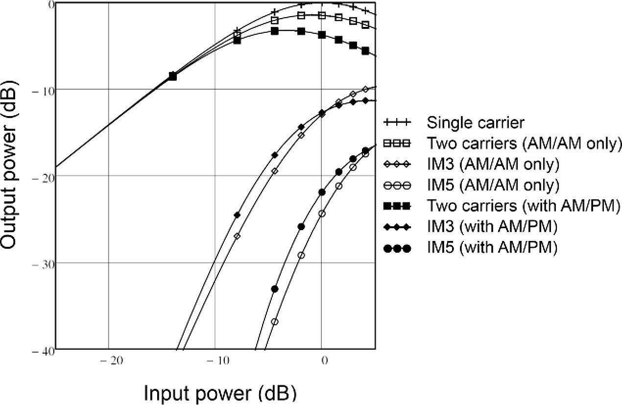
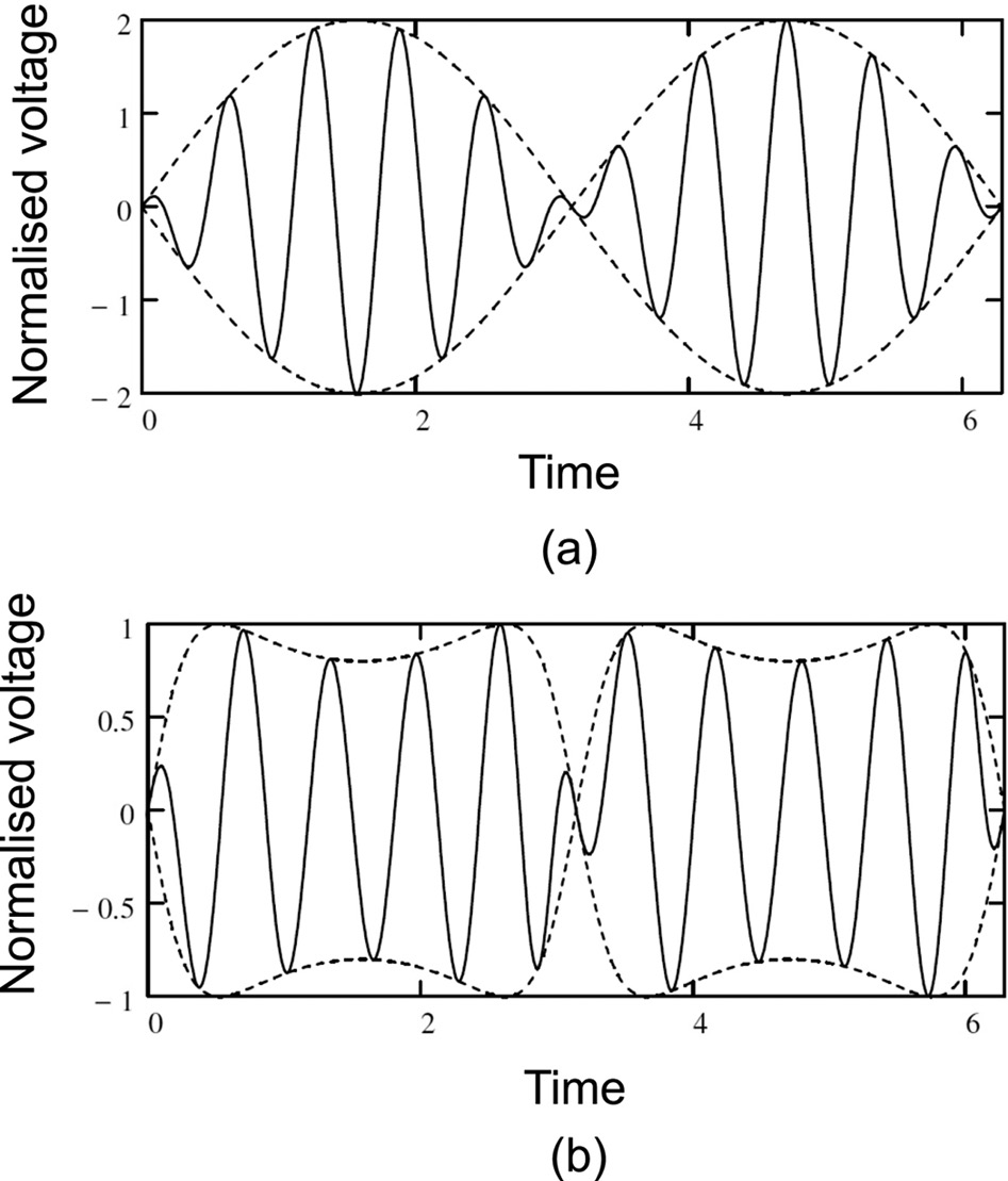
  . This power can be plotted against the RF input power for comparison with the single-carrier AM/AM characteristic as shown in Figure 1.15. At small input powers the amplifier is linear and the power gain is identical to that with one carrier. However, as the input power approaches the single-carrier saturation level the output power is less with two carriers than with one. The reason for this is illustrated in Figure 1.16 which shows typical two-tone input and output waveforms for an amplifier, normalised to the saturated output voltage of the amplifier. For clarity of explanation the carrier frequency shown is much lower relative to the frequency of the envelope than would normally be the case. The output voltage is reduced when the instantaneous amplitude of the signal exceeds the saturation level of the amplifier. Thus the saturated output power under multi-carrier operation is less than that for a single carrier at the same input power. Figure 1.15 also compares the effects of AM/AM conversion alone (typical of klystrons) with those in which AM/PM conversion is also included (typical of TWTs) [Reference Stette45].

Figure 1.15: Typical AM/AM transfer characteristics for two-carrier operation showing third-order (IM3) and fifth-order (IM5) intermodulation products.

Figure 1.16: Typical waveforms for two-carrier operation of a non-linear amplifier: (a) input, and (b) output.
When we set  and
and  in (1.52) we obtain a third-order intermodulation product at frequency
  whose amplitude is
 (1.54)
In the same way, setting  and
and  gives a fifth-order intermodulation product at
  whose amplitude is
 (1.55)
The amplitudes of the other intermodulation products at  and
and  are the same. Then the total third-order (IM3) and fifth-order (IM5) intermodulation powers can be plotted as shown in Figure 1.15. The frequencies of these signals coincide with those of possible adjacent carriers resulting in co-channel interference. The acceptable level of interference is commonly expressed as the ratio
  of the fundamental power to that of the third-order intermodulation product, expressed in decibels. At low drive levels the slope of the graph of the third-order product is 3 dB/dB and that of the fifth-order product is 5 dB/dB. Thus the ratio
  can be increased by operating the amplifier at a reduced drive level. This is commonly expressed in terms of the output back-off from saturation (in dB) necessary to achieve an acceptable value of
  . The linear parts of the curves for the intermodulation products can be extrapolated in the same manner as in Figure 1.4 to meet the extrapolation of the fundamental curve at the third-order and fifth-order intercept points. These may also be used to specify the linearity of the amplifier.
The functions A and  required for the evaluation of the integrals in (1.53) to (1.55) may be specified numerically using interpolation on data points which have been determined experimentally or by large-signal modelling [Reference Stette45]. Alternatively a suitable function may be fitted to the data points [Reference Berman and Mahle42, Reference Saleh43, Reference Kunz46]. Polynomial expansions do not give a good fit to the data unless a large number of terms is used. In particular these models fail for drive levels approaching saturation. They do, however, reveal that the fundamental, and intermodulation, amplitudes depend only on the odd terms of the series. These can be specified independently of the terms describing the dependence of the even harmonics on the input RF power [Reference Kunz46]. Simple functions which are a good fit to experimental data for TWTs have been proposed by Saleh [Reference Saleh43]:
 (1.56)
and
 (1.57)
where  ,
,  ,
,  and
and  are empirical constants. If the amplifier has unity gain at saturation, so that
  , it can be shown that
  and
and  . These values are close to the empirical figures so that it is possible to use them as a useful approximation. In the same way it may be tentatively suggested that the function required to generate the even harmonics might be written
 (1.58)
The curves shown in Figures 1.4 and 1.15 were generated using this non-linear model (see Worksheet 1.3).
The ratio  is commonly used for specifying the intermodulation distortion in an amplifier, not least because it is straightforward to measure it experimentally. However, it is at best, a proxy for the intermodulation effects because, when there are more than two carriers, the overall performance depends upon the signal levels of all the carriers. Since the phases of the phase-modulated carriers vary in a quasi-random manner it may be assumed that all phase combinations are equally probable. Where only two carriers are used it is sufficient to consider unmodulated sine waves because all possible phases arise in one period of the difference frequency. Then the peak power is twice the mean power. However, with three or more carriers this is not the case, and it is necessary to use Monte Carlo methods to examine all possible phases [Reference Carter47]. As the number of carriers increases, the probability that all the signals will be in phase simultaneously decreases. In the limit, a large number of uncorrelated phase-modulated carriers can be represented by band-limited white noise [Reference Stette45, Reference Guida48]. This leads to an alternative measure of intermodulation distortion in which the input to the amplifier is band-limited white noise from which the portion in a small frequency range has been removed by a notch filter. The non-linearity of the amplifier causes some signals to be generated in this frequency range. The ratio of the amplitude of these to that of the white noise at the output of the amplifier is the Noise Power Ratio (in dB). This is a measure of the level of interference which would be experienced by a signal at the centre of the notch [Reference Reveyrand49, Reference Katz and Gray50]. An approximation to this can be achieved experimentally, or in simulations, by using a comb of carriers at equal frequency intervals such that one carrier has been omitted from the centre of the set as shown in Figure 1.17(a) [Reference Carter47, Reference Loo51]. Figure 17(b) shows a typical output spectrum and the definition of the noise power ratio. Intermodulation products are also generated on the edges of the input spectrum so increasing its bandwidth. If the power in these is great enough then it may cause interference with other systems operating in adjacent frequency bands. For this reason the permitted bandwidth may be expressed as a spectrum envelope [Reference Amoroso52].

1.7 Engineering Design
The design of any engineering product can be divided into three phases:
i) Conceptual design, in which the principal dimensions and operating parameters are established.
ii) Detailed design, involving refinement of the conceptual design by prototyping and advanced modelling, leading to the preparation of the manufacturing data package and the test specification.
iii) Design consolidation, incorporating further refinements suggested by product testing and field experience.
The costs that are committed, and incurred, increase at each stage. It is therefore desirable to produce a conceptual design which does not require further modification at the detailed design stage; and a detailed design which does not have to be modified as a result of unsatisfactory performance in the field. It should be noted that performance and environmental testing is normally carried out under laboratory conditions, and care must be taken to ensure that tubes which pass these tests do also perform well in the field. Differences between the testing and the real environments, such as the impedances of power supplies and matches of RF components, can affect how a tube performs.
1.7.1 Dimensionless Parameters and Scaling
Nearly all tubes are developed in organisations in which the design process can be based upon accumulated knowledge and expertise. Many tubes are designed by scaling from existing designs, or by other modifications to them, rather than starting from a clean sheet of paper. It is, however, important that this process should be underpinned by fundamental understanding.
The basis for scaling is dimensional analysis [Reference Buckingham53, Reference Wilson54]. Let us suppose that some aspect of the performance of a tube is governed by an equation which can be written in the general form
 (1.59)
where  are dimensional variables and
  are dimensionless ratios. Very commonly these are the ratios of the leading dimensions of the tube to a single dimension or to a dimensional variable such as the free-space wavelength. If two tubes are described by the same set of dimensionless ratios, so that all dimensions are changed by the same multiplying factor, they are said to be geometrically similar to one another. If geometrical similarity is assumed then the ratios are constants and (1.59) can be written
 (1.60)
This equation is a complete description of the problem, provided that none of the variables required has been overlooked. The choice of variable for inclusion is based upon an understanding of the physics of the problem. When it involves electromagnetics then the primary electric and magnetic constants  and
and  may have to be included in the list. The ratio of the charge to the rest mass of an electron
  is also required when the dynamics of electrons are part of the problem. Equation (1.60) remains valid even if the algebraic form of the function is unknown. The dimensions of the variables
  can be expressed in terms of the fundamental dimensions mass [M], length [L], and time [T], together with voltage [V] or charge for electrical problems. Thus there are, at most, four fundamental dimensions. Table 1.7 shows the dimensions of some quantities relevant to vacuum tubes.
Table 1.7: Typical independent and dependent parameters for vacuum tubes
| Parameter | Dimensions | |
|---|---|---|
| Constants | Velocity of light in free space (c) 0.299792 × 10⁹ m s−1 |  |
Primary electric constant  8.854187 × 10⁻¹² F m−1 |  | |
Primary magnetic constant  1.256637 × 10⁻⁶ H m−1 |  | |
| Elementary charge (e) 1.602176 × 10⁻¹⁹ C |  | |
| Rest mass of the electron (m0) 9.109382 × 10⁻³¹ kg 0.510998 MeV |  | |
Electron charge to mass ratio  1.758820 × 10¹¹ C kg−1 |  | |
| Parameters | Length |  |
| Voltage |  | |
| Magnetic flux density |  | |
| Frequency |  | |
| R.F. power |  | |
| Current |  | |
| Electron velocity |  | |
| Charge density |  |
The variables Q may be combined together to form dimensionless groups denoted by  so that (1.60) can be written
 (1.61)
The number of groups required is related to the number of variables by
 (1.62)
where k is the number of dimensions required. This is known as Buckingham’s theorem. An immediate effect of using dimensionless variables (or dimensionless groups) is that the number of variables required to define the problem has been reduced. Now let us choose one of the groups to be a dependent variable whose value is determined by the values of the others. Then (1.61) becomes
 (1.63)
If the values of the independent variables  are fixed then so is the value of the dependent variable
  . Two tubes which are described by the same values of the dimensionless variables are said to be dynamically similar to one another. Thus the basis of scaling is the maintenance of both geometrical and dynamic similarity.
The process of forming dimensionless groups is aided by choosing normalisations which are based on the underlying physics of the problem. Some examples are shown in Table 1.8.
Table 1.8: Examples of the formation of dimensionless groups
| Variable | Normalising quantity | Dimensionless group |
|---|---|---|
| Dimension (d) | Wavelength  Propagation constant  |  or or  |
| Velocity (u) | Velocity of light (c) Phase velocity  |  or or  |
| Voltage (V) | Rest energy of the electron in eV  |  |
Electron plasma frequency  Electron cyclotron frequency  | Frequency  |  and and  |
A simple illustration is provided by the calculation of the velocity of an electron  from an applied voltage
  and the dimensional constants. The dependent dimensionless group is
 (1.64)
and the independent dimensionless group is
 (1.65)
In this case there are five parameters and three independent dimensions:  ,
,  and
and  so that the problem is completely described by the two dimensionless groups which have been formed. Note that in this case the dimensions
  and
and  do not occur separately so that the number of independent dimensions is reduced by one. It follows that we can write
 (1.66)
where  is an unknown function which can be determined empirically, even if its form cannot be found by mathematical analysis. The value of the reduction of the description of a problem to the form in (1.63) is greater than just that of scaling. If the form of the function
  is known, even over a limited range of variation of the variables then it can be used to explore the effects of design choices on
  . In cases where geometrical similarity is not maintained then one, or more, of the ratios r are added as dimensionless variables. Examples of the application of this method to particular problems in tube design are given later in this book.
1.7.2 Modelling
The trend in tube design is towards achieving near-ideal RF performance coupled with high reliability and low cost of ownership. For this reason, the design of a state-of-the-art vacuum tube is a complex business which involves considerable use of computer simulations to achieve right-first-time design [Reference Antonsen55, Reference Carter56]. The advanced computer codes used for detailed design can take many hours to run, even on the most powerful computers available. They are invaluable tools for accurate modelling, but are not well-suited to the conceptual design stage which is the focus of this book. For that, the engineers must have a sound understanding of the theory of vacuum tubes, together with simple computer models which can be used for rapid design iterations.
The availability of advanced computer modelling tools such as Particle in Cell (PIC) codes can mislead the unwary into supposing that the best way of modelling a tube is to create a complete model in such a code. This approach is wrong on two counts:
i) A PIC code finds a self-consistent numerical solution of Maxwell’s equations and the equations of motion in a series of time steps. However, the solution is linear in the part of the problem space which is not occupied by electrons. It is therefore more efficient to compute that part of the solution once and store it for future use. The problem is then reduced to the solution of the non-linear model in the space containing electrons, subject to matching the stored solution on the boundary. This is the method used in the large-signal models of tubes which are described later in this book.
ii) Even the best computer codes cannot be wholly accurate models of reality because the complexity of the problem is too great, so that some parts of it may not be known precisely. Assumptions and approximations are always required. For this reason the mathematical modelling of tubes is as much an art as it is a science [Reference Johns57]. The best results are obtained when the physics of the problem are well understood so that the assumptions and approximations are valid. Any model is only useful when it has been validated by comparison with experimental results. Even then it can only be used with caution outside the range of parameters for which it has been validated.
A large number of simple models were created in Mathcad14® during the writing of the book and used to generate many of the figures. These models can be used to explore the behaviour of different aspects of tubes by changing the parameters. They are available in electronic form (see the list of worksheets in the Appendix, available online at www.cambridge.org/9780521198622). The comments included in them should be sufficient for users to create their own models using other software if they wish. The models are intended as educational tools and have not been validated for use in tube design.