To save content items to your account,
please confirm that you agree to abide by our usage policies.
If this is the first time you use this feature, you will be asked to authorise Cambridge Core to connect with your account.
Find out more about saving content to .
To save content items to your Kindle, first ensure no-reply@cambridge.org
is added to your Approved Personal Document E-mail List under your Personal Document Settings
on the Manage Your Content and Devices page of your Amazon account. Then enter the ‘name’ part
of your Kindle email address below.
Find out more about saving to your Kindle.
Note you can select to save to either the @free.kindle.com or @kindle.com variations.
‘@free.kindle.com’ emails are free but can only be saved to your device when it is connected to wi-fi.
‘@kindle.com’ emails can be delivered even when you are not connected to wi-fi, but note that service fees apply.
A new method for photopatterning of a bisanthracene-functionalized mesogenic compound 1 was developed. The monomer 1 had two anthracene moieties on each molecular end, and showed crystalline and liquid-crystalline phases at room temperature and at an elevated temperature, respectively. Upon UV irradiation of 1 in the molten state, intermolecular photodimerization of the anthracene moieties was induced, and consequently resulted in the formation of a linear polymer. In contrast to the monomer 1, the obtained polymer exhibited amorphous phase at room temperature. When 1 was irradiated with UV light through a photomask in the molten state, the irradiated areas changed to amorphous phase due to photopolymerization, whereas the non-irradiated areas remained the ordered phase. This phenomenon provided visual images with a clear contrast under polarized light. In addition, the images could be erased by heating the whole sample at a temperature above ca. 200 °C, because the amorphous phase changed to the ordered phase due to a reproduction of the monomer 1 from the polymer associated with thermal back-reaction of the anthracene photodimer. Photopatterning could be performed for the erased sample again and the process was found to be fairly reversible.
Titanium alloys are among the most used metallic biomaterials, particularly for orthopedic applications. Ever since the pioneer titanium alloy (Ti6Al4V) has been used as biomaterial, lack of biocompatibility has been extensively reported and propelled research on improved materials with appropriate mechanical behavior and adequate biocompatibility. Studies have indicated that vanadium produces oxides harmful to the human body; in order to replace vanadium containing Ti alloys, Ti-6Al-7Nb was developed. Today this alloy is the preferred choice for cementless total joint replacements. It is very important to produce a nanostructured bioactive metal implant with appropriate mechanical properties and we applied a chemical and thermal treatment that converts the surface of titanium alloy into bioactive surface. Therefore, bioactive Ti6Al7Nb might represent an alternative for advanced orthopedic implants under load-bearing conditions.
Eleven mini-pigs weighting around 50 kg, with free access to food pellets and water, were the experimental animals for this study. Ten of these pigs (one is the control) were anesthetized and after shaving, disinfection and draping, a straight 3 cm incision was made and the implants (plate and pin) were implanted into the epiphyses of the tibiae. Surgical procedures were performed bilaterally. At 6 months after implantation, the mini-pigs were sacrificed.
After sacrifice, the segments of the proximal tibia epiphyses containing the implanted plates and pins were cut of, fixed in phosphate-buffered formalin and dehydrated in serial concentrations of ethanol after which they were embedded in polyester resin and then cutted and grounded to a thickness of 75-100 μm. With these samples a lot of observations were made: Scanning Electron Microscopy observations, histological examination at implant surface and histological examination of the bone-implant surface and SEM-EDX examinations were also made.
All the results revealed that the plates and pins are in direct contact with newly formed bone without any intervening soft tissue layer. We regard osteoinductive ability of nanostructured Ti6Al7Nb as one of the advantages of this implant in consideration for clinical applications.
An oxide dispersion strengthened steel is produced which contains Y-Al-Ti-O nanoparticles with an average diameter of 21 nm. HRTEM analysis shows that the chemical composition of the Y2O3 oxide is modified with perovskite YAlO3 (YAP), Y2Al5O12 garnet (YAG) and Y4Al2O9 monoclinic (YAM) particles. Irradiation of these alloys was performed with a dual ion beam system operating simultaneously with 2.5 MeV Fe+ to 31 dpa and 350 keV He+ to 18 appm/dpa. Ion bombardment causes atomic displacements resulting in vacancy and self-interstitial lattice defects and dislocation loops. TRIM calculations for ODS steel indicate a clear spacial separation between vacancies and self-interstitials at which the vacancy distribution is close to the surface and the interstitials are deposited at a deeper position. The helium atoms mainly accumulate in the vacancies. Fine He cavities with diameters of a few nanometers were identified in HRTEM images. Additionally to structural changes, irradiation generated defects also affect the mechanical properties of the ODS steel. These were investigated by nanoindentation, which is a suitable measuring method as the irradiation damage is created within a thin surface layer. A clear hardness increase in the irradiated depth region was observed, which reaches a maximum close to the surface. This indicates the He condensation in the vacancy dominated region predicted by the simulations.
A fundamental understanding of the radiation damage effects in solids is of great importance in assisting the development of improved materials with ultra-high strength, toughness, and radiation resistance for nuclear energy applications. In this presentation, we show our recent theoretical investigation on the magnetic structure evolution of bulk iron in the region surrounding the radiation defects. We applied the locally self-consistent multiple scattering method (LSMS), a linear scaling ab-initio method based on density functional theory with local spin density approximation, to the study of the magnetic structure in a low energy cascade in a 10,000-atom sample for a series of time steps for the evolution of the defects. The primary damage state and the evolution of all defects in the sample were simulated using molecular dynamics with empirical, embedded-atom inter-atomic potentials. We also discuss the importance of thermal effect on the magnetic structure evolution.
We carried out a systematic experimental study of the low-frequency noise characteristics in a large number of single and bilayer graphene transistors. The prime purpose was to determine the dominant noise sources in these devices and the effect of aging on the current-voltage and noise characteristics. The analysis of the noise spectral density dependence on the surface area of the graphene channel indicates that the dominant contributions to the 1/f electronic noise come from the graphene channel region itself. Aging of graphene transistors due to exposure to ambient for over a month resulted in substantially increased noise, which was attributed to the decreasing mobility of graphene and increasing contact resistance. The noise spectral density in both single and bilayer graphene transistors shows a non-monotonic dependence on the gate bias. This observation confirms that the 1/f noise characteristics of graphene transistors are qualitatively different from those of conventional silicon metal-oxide-semiconductor field-effect transistors.
Thick (>150 μm) beryllium coatings are studied as an ablator material of interest for fusion fuel capsules for the National Ignition Facility (NIF). As an added complication, the coatings are deposited on mm-scale spherical substrates, as opposed to flats. DC magnetron sputtering is used because of the relative controllability of the processing temperature and energy of the deposits. We used ultra small angle x-ray spectroscopy (USAXS) to characterize the void fraction and distribution along the spherical surface. We investigated the void structure using a combination focused ion beam (FIB) and scanning electron microscope (SEM), along with transmission electron microscopy (TEM). Our results show a few volume percent of voids and a typical void diameter of less than two hundred nanometers. Understanding how the stresses in the deposited material develop with thickness is important so that we can minimize film cracking and delamination. To that end, an in-situ multiple optical beam stress sensor (MOSS) was used to measure the stress behavior of thick Beryllium coatings on flat substrates as the material was being deposited. We will show how the film stress saturates with thickness and changes with pressure.
Aluminosilicate aerogels offer potential for extremely low thermal conductivities at temperatures greater than 900°C, beyond where silica aerogels reach their upper temperature limits. Aerogels have been synthesized at various Al:Si ratios, including mullite compositions, using Boehmite (AlOOH) as the Al source, and tetraethoxy orthosilicate as the Si precursor. The Boehmite-derived aerogels are found to form by a self-assembly process of AlOOH crystallites, with Si-O groups on the surface of an alumina skeleton. Morphology, surface area and pore size varies with the crystallite size of the starting Boehmite powder, as well as with synthesis parameters.
Ternary systems, including Al-Si-Ti aerogels incorporating a soluble Ti precursor, are possible with careful control of pH. The addition of Ti influences sol viscosity, gelation time pore structure and pore size distribution, as well as phase formation on heat treatment.
Mechanical energy harvesting from ambient vibrations is an attractive renewable source of energy for various applications. Prior research was solely based on lead-containing materials which are detrimental to the environment and health. Therefore, lead-free materials are becoming more attractive for harvesting applications. The present work is focused on the development of lead-free piezoelectric materials based on solid solution having composition (KNa)NbO3-xABO3, (where A = Li, and B = Nb; x = 0, 5, 5.5, 6, and 6.5 wt%). The solid solutions of the above ceramics were prepared by using solid-state reaction method. The X-ray diffraction spectra exhibited single phase formation and good crystallinity with LiNbO3 addition up to x = 6.5 wt%. Dielectric studies reveal that the composition with LiNbO3 = 6.5 wt% exhibits superior properties suitable for piezoelectric energy harvesting applications. The nanoscale piezoelectric data obtained with piezoresponse force microscopy provide a direct evidence of strong piezoelectricity with LN doping. The best piezoelectric properties are obtained for the composition K0.5Na0.5NbO3 – 6.5%LiNbO3.
The paper presents a rate-independent dislocation growth and defect annihilation mechanism to capture the pre- and post-yield material behavior of FCC metals subjected to different doses of neutron radiation. Based on observation from molecular dynamics simulation and TEM experiments, the developed model is capable of capturing the salient features of irradiation induced hardening including increase in yield stress followed by yield drop and non-zero stress offset from the unirradiated stress-strain curve. The key contribution is a model for the critical resolved slip resistance that depends on both dislocation and defect densities which are governed by evolution equations based on physical observations. The result is an orientation-dependent nonhomogeneous deformation model which accounts for defect annihilation on active slip planes. Results for both single and polycrystalline simulations of OFHC copper are presented and are observed to be in reasonably good agreement with experimental data. Extension of the model to other FCC metals is straightforward and is currently being developed for BCC metals giving its way for generation of new materials.
The crystallographic texture of lead zirconate titanate (PZT) thin films strongly influences the piezoelectric properties used in MEMS applications. For PZT films poled to saturation, the piezoelectric response is sequentially greater for random, {111}, and {001} texture. Textured growth can be achieved by relying on crystal growth habit and can also be initiated by the use of a seed layer that provides a heteroepitaxial template. Template choice and the process used to form it determine the structural quality and ultimately influence performance and reliability of MEMS PZT devices such as switches, filters, and actuators. This study focuses on how {111}-textured PZT is generated by a combination of crystal habit and templating mechanisms that occur in the PZT/bottom-electrode stack. The sequence begins with {0001}-textured Ti deposited on thermally grown SiO2 on a Si wafer. The Ti is converted to {100}-textured TiO2 (rutile) through thermal oxidation. Then {111}-textured Pt can be grown to act as a template for {111}-textured PZT. The Ti and Pt are deposited by DC magnetron sputtering. The TiO2 and Pt film textures and structure were optimized by variation of sputtering deposition times, temperatures and power levels, and post-deposition anneal conditions. The relationship between Ti, TiO2, and Pt texture and their impact on PZT growth will be presented.
Organic materials have been widely used in various fields of electronic applications. However, they are difficult to process without damage by using a conventional ion beam which use energetic ions. In this study, gas cluster ion beam (GCIB), which shows low-damage process, was used for organic materials, and irradiation effect of size selected GCIB was studied with Xray photoelectron spectroscopy (XPS). In the case of irradiation of 500 eV Ar ion (monomer ion) on polyimide, the intensities of both N-C=O and C-O bond decreased after irradiation. On the other hand, there was small change in the XPS spectra after 15 keV Ar-GCIB irradiation with the same ion dose. The etching rate of polyimide per one ion with 15 keV Ar-GCIB was almost 1.8×10⁴ times higher than that with 500 eV Ar monomer ions. The damages in polyimide decreased with increasing the Ar cluster size owing to the reduction of energy per atom at acceleration voltage of 15 kV. After irradiation of size selected 5 kV Ar cluster ion, damage was almost negligible. Although, the surface became rough after irradiation of Ar-GCIB, surface roughness and the change of chemical bond were very small with N2-GCIB irradiation. Ar-GCIB irradiation on dye-sensitized solar cells (N719) showed that very low-damage process is possible with GCIB, and it indicated that GCIB is suitable for surface processing of organic materials used in electronic devices.
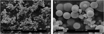
Three-dimensional (3D) sphere-like Eu3+-doped white light lutetium tungstate phosphors have been fabricated by the cationic surfactant cetyltrimethyl ammonium bromide (CTAB)-assisted hydrothermal method, which presents a diameter of ∼2-μm morphology assembled by nanoflakes with a length of 100 to ∼200 nm. The results demonstrate that CTAB, suitable pH values, reaction time, and reaction temperature are all essential for the formation of lutetium tungstate microspheres. Photoluminescence measurement indicates that lutetium tungstate microspheres show a broad O–W Charge transfer state (CTS) transition and the characteristic emission of Eu3+ at ∼591 and ∼611 nm.
We investigated, by employing a photoluminescence technique, the etching damage introduced in near-surface regions of GaN by Ar and Kr plasmas and clarified the differences between the damage characteristics of these regions for the two plasma etching cases. For Ar plasma, the shallow donor-acceptor pair emission at ~3.28 eV was significantly weakened; additionally, a broad blue luminescence band arose at approximately ~3.0 eV. In contrast, for Kr plasma under high gas pressure, we found the recovery of the damage to the same level as the as-grown crystallinity. These differences in the damage characteristics for the two plasma etching cases probably depend upon which atom (N or Ga) is preferentially etched in these cases.
In this work hydrophobicaly ligated cadmium selenide/zinc sulfide CdSe/ZnS quantum dots (QDs) were incorporated in transparent matrices by formation of CdSe/ZnS/SiO2 core/shell/shell structure using microemolsion synthesis method. The optical properties of the QDs encapsulated with a chemically grown oxide layers were studied. Intense luminescence properties of the QD/silica nanoparticles (NPs) were observed using steady state photoluminescence (PL) measurements. Confocal microscopy demonstrates fluorescence of the single core/shell/shell nanoparticles. The obtained results along with the Secondary Electron Microscopy (SEM) and Transmission Electron Microscopy (TEM) images provide information on the geometry of the QDs. The excitonic emission of nanoparticles was also mapped using a liquid nitrogen cryostat the 77K - 300K range. The temperature dependent PL spectra of the film demonstrate the temperature-dependent band gap shrinkage of the QDs. PL lifetime measurements were performed on the ensemble of NPs. Experimental data was fitted to the numerical model with lifetime constants in nanoseconds range. We demonstrate that the main nonradiative processes that limit the quantum yield (QY) of the QDs at room temperature are the carrier trapping at the interface of QD/silica and the exciton-phonon coupling. These studies give us insight to exploit the QD layers for photon down shifting and multiple exciton generation for application in photovoltaics.
Graphene oxide (GO) is a nonstoichiometric two-dimensional material obtained from the chemical oxidation and exfoliation of graphite, which has recently attracted intense research interest as a precursor for bulk production of graphene. GO has long been believed to be hydrophilic due to its dispersibility in water. Recent work in our group, however, has found that GO is actually a two-dimensional amphiphile; the edge of the sheet-like material is hydrophilic, while the basal plane of the material contains more hydrophobic graphitic nanodomains. To prove the concept, we demonstrate GO’s surface activity at an air-water interface, as well as its utility in dispersing insoluble aromatic materials such as toluene, graphite, and carbon nanotubes in water. As a colloidal surfactant which can be converted to a conducting material, GO presents unique possibilities for aqueous solution processing of organic electronic materials.
Ferroelectric field effect transistor (FFET) is a promising candidate for non-volatile random access memory because of its high speed, single device structure, low power consumption, and nondestructive read-out operation. Currently, however, such ideal devices are commercially not available due to poor interface properties between ferroelectric film and Si substrate, such as leakage current and interdiffusion etc. So we choose YSZ and HfO2 insulating thin films as buffer layer due to they possess relatively high dielectric constant, high thermal stability, low leakage current, and good interface property with Si substrates. Two structural diodes of Pt/BNT/YSZ/Si and Pt/SBT/HfO2/Si were fabricated, and the microstructures, interface properties, C-V, I-V, and retention properties were investigated in detail. Experimental results show that the fabricated diodes exhibit excellent long-term retention properties, which is due to the good interface and the low leakage density, demonstrating that the YSZ and HfO2 buffer layers are playing a critical modulation role between the ferroelectric thin film and Si substrate.
We investigated temperature dependence of the electrical conductance ofsingle oligothiophene molecular wires with the length of 2.2 nm (5-mer), 5.6nm (14-mer) and 6.7 nm (17-mer) by using the scanning tunneling microscopybreak junction method. Results show that the dominant charge carriertransport for 5-mer molecule is tunneling while for 17-mer molecule ishopping. The carrier transport mechanism of 14-mer are tunneling transport(T ≤ 350 K) and hopping transport (T > 350 K) indicating that hopping andtunnelling transport are competitive process in the molecular junction.
In the work presented here atomic force microscopy (AFM) based mechanical mapping techniques - HarmoniX imaging and Peak Force Tapping - were applied to determine the surface elastic modulus of phase separated polyurethanes and silica reinforced rubbers across the length scales. Segmented polyether polyurethanes (PUs) were prepared with varying stoichiometric ratio of the isocyanate and hydroxyl groups. The effect of molar mass, as well as the type and number of end-groups on their morphology was investigated. Smooth PU samples for AFM imaging were prepared by ultramicrotonomy. The micro phase separated morphology of the phase separated PUs showed characteristic “fingerprint” AFM phase images. Surface modulus values obtained by AFM were compared to bulk modulus values obtained by tensile testing. The moduli were mapped quantitatively with nanoscale resolution and were in excellent agreement for both AFM modes. Surface mean moduli values do not coincide with bulk values obtained via tensile testing which is attributed to fundamentally different averaging procedures and effects that lead to the respective modulus values obtained via surface and volume averaging. EPDM and SBR rubbers and rubber blends thereof were prepared with varying concentrations of silica nanoparticles and studied in order to investigate the effect of different composition on the resulting morphology (filler distribution) and elastic moduli on a specific rubber or rubber blend sample. Elastic moduli of the rubber and rubber blend samples were first measured by bulk tensile testing. The morphology of the rubber samples was visualized by height and phase imaging. Surface elastic moduli of silica reinforced rubbers and rubber blends were mapped quantitatively and compared with bulk tensile test results. AFM allowed the determination of modulus distributions at the sections imaged. As potential reasons for the observed differences between bulk and surface modulus different averaging procedures like surface and bulk averaging of AFM vs. tensile testing, different filler distributions in SBR and EPDM and the AFM modulus calibration procedures can be named.
High quality ZnO:Al (AZO) thin films were prepared on glass substrates by direct current filtered cathodic arc deposition. Substrate temperature was varied from room temperature to 425°C, and samples were grown with and without the assistance of low power oxygen plasma (75W). For each growth condition, at least 3 samples were grown to give a statistical look at the effect of the growth environment on the film properties and to explore the reproducibility of the technique. Growth rate was in the 100-400 nm/min range but was apparently random and could not be easily traced to the growth conditions explored. For optimized growth conditions, 300-600 nm AZO films had resistivities of 3-6 x 10⁻⁴ Ωcm, carrier concentrations in the range of 2-4 x 1020 cm3, Hall mobility as high as 55 cm2/Vs, and optical transmittance greater than 90%. These films are also highly oriented with the c-axis perpendicular to the substrate and a surface roughness of 2-4 nm.
ZnO/Ta2O5 heterojunctions were formed on glass substrates using low temperature processes. Formerly insulating Ta2O5 films were deposited on glass substrates by vacuum evaporation using Ta2O5 powder, Afterwards transparent and conductive ZnO films were formed on the Ta2O5 films by thermal oxidation at 3200C in air atmosphere of zinc (Zn) films deposited by dc sputtering process. Structural and optical properties of ZnO were investigated by X-ray diffraction (XRD) and photoluminescence (PL). The Ta2O5 insulating films were characterized by Raman scattering. The ZnO/Ta2O5 heterojunction was characterized by current-voltage measurements at room temperature as well as transient response under a rectangular-pulse voltage source. The electrical and the transient response suggest that the ZnO/Ta2O5 heterojunction is a potential alternative for the fabrication of alternating-current-driven thin film electroluminescent (ACTFEL) devices.