To save content items to your account,
please confirm that you agree to abide by our usage policies.
If this is the first time you use this feature, you will be asked to authorise Cambridge Core to connect with your account.
Find out more about saving content to .
To save content items to your Kindle, first ensure no-reply@cambridge.org
is added to your Approved Personal Document E-mail List under your Personal Document Settings
on the Manage Your Content and Devices page of your Amazon account. Then enter the ‘name’ part
of your Kindle email address below.
Find out more about saving to your Kindle.
Note you can select to save to either the @free.kindle.com or @kindle.com variations.
‘@free.kindle.com’ emails are free but can only be saved to your device when it is connected to wi-fi.
‘@kindle.com’ emails can be delivered even when you are not connected to wi-fi, but note that service fees apply.
We synthesize a series of polyvinylcarbazole (PVK) monoliths containing varying loadings of triphenyl bismuth as a high-Z dopant and varying fluors, either organic or organometallic, in order to study their use as scintillators capable of gamma ray spectroscopy. A trend of increasing bismuth loading resulting in a better resolved photopeak is observed. For PVK parts with no fluor or a standard organic fluor, diphenylanthracene (DPA), increasing bismuth loading results in decreasing light yield while with samples 1 or 3 % by weight of the triplet harvesting organometallic fluor bis(4,6-difluoropyridinato-N,C2)picolinatoiridium (FIrpic) show increasing light yield with increasing bismuth loading. Our best performing PVK/ BiPh3/FIrpic scintillator with 40 wt % BiPh3 and 3 wt % FIrpic has an emission maximum of 500 nm, a light yield of ∼30,000 photons/MeV, and energy resolution better than 7% FWHM at 662 keV. Replacing the Ir complex with an equal weight of DPA produces a sample with a light yield of ∼6,000 photons/MeV, with an emission maximum at 420 nm and energy resolution of 9% at 662 keV. Transmission electron microscopy studies show that the BiPh3 forms small clusters of approximately 5 nm diameter.
Hydrogen (H2) sensing property of AgInSbTe (AIST)-SiO2 nanocomposite thin film prepared by target-attachment sputtering method was investigated in this work. The sample subjected to a 400°C-annealing for 90 sec exhibits a significant sensitivity (58.9 %) and short response time (75 sec) upon the exposure to an ambient containing 200 ppm H2 at 75°C. The gas sensing capability is ascribed to the presence of antimony oxides, e.g., Sb2O3 and Sb2O5, in nanocomposite layer which provide the charge carriers for sensing reactions. Moreover, the high specific-surface-area (SSA) feature of AIST nanocrystals in nanocomoposite layer provided numerous sites for reduction/oxidation reactions and thus a good H2 gas sensing property can be achieved.
Graphitic nanomaterials such as graphene, carbon nanotubes (CNT), and C60 fullerenes are promising materials for energy applications because of their extraordinary electrical and optical properties. However, graphitic materials are not readily dispersible in water. Strategies to fabricate all-carbon nanocomposites typically involve covalent linking or surface functionalization, which breaks the conjugated electronic networks or contaminates functional carbon surfaces. Here, we demonstrate a facile surfactant-free strategy to create such all-carbon composites. Fullerenes, unfunctionalized single walled carbon nanotubes, and graphene oxide sheets can be conveniently co-assembled in water, resulting in a stable colloidal dispersion amenable to thin film processing. The thin film composite can be made conductive by mild thermal heating. Photovoltaic devices fabricated using the all-carbon composite as the active layer demonstrated an on-off ratio of nearly 106, an open circuit voltage of 0.59V, and a power conversion efficiency of 0.21%. This photoconductive and photovoltaic response is unprecedented among all-carbon based materials. Therefore, this surfactant-free, aqueous based approach to making all-carbon composites is promising for applications in optoelectronic devices.
Metal organic framework (MOF) materials are a class of hybrid organic-inorganic crystalline materials whose pore structures and chemical properties can be tailored by the selection of component chemical moieties. Many MOFs have extraordinary intrinsic surface areas, capable of adsorbing large quantities of other chemicals, such as volatile organic compounds or moisture. Upon absorption of guest molecules, many MOFs undergo reversible changes in the dimensions of their unit cells. These properties suggest several routes to chemical sensing in which the transduction mechanisms are: 1) the stress induced at an interface between a flexible MOF layer and a static microcantilever fabricated with a built-in piezoresistive stress sensor; 2) the change in the resonant frequency of an oscillating microcantilever induced by mass adsorption; and 3) the change in the resonant frequency of a acoustic sensor, such as a surface acoustic wave (SAW) sensor through changes in mass loading and film moduli. This paper focuses on humidity sensing by SAWs coated with Cu3(BTC)2 (HKUST-1) over a very broad concentration range.
Sandia National Laboratories is a multi-program laboratory managed and operated by Sandia Corporation, a wholly owned subsidiary of Lockheed Martin Corporation, for the U.S. Department of Energy’s National Nuclear Security Administration under contract DE-AC04-94AL85000.
The goal in this study was to synthesize a lanthanum - nickel phase (Ruddlesden-Popper phases) La4Ni3O10. This material was prepared using a polymeric route. An easy synthesis method is presented in order to obtain an economical cathode material, which can be used in Solid Oxide Fuel Cells (SOFC). The polymeric precursors were prepared following the Castillo method. The originality of this work was to optimize the ratio HMTA/ metallic salts from 1 to 6. The obtained powders were characterized by thermal analysis; Differential Scanning Calorimetry (DSC Q10 Instrument TA), Thermogravimetric Analysis (TGA - Q50 Instrument TA-) and X-ray diffractometer (Bruker, D8 Advance diffractometer), in order to determine the crystallized phase. Experiments 5 and 6 did not present coagulation but after few days, solution 5 was transformed into a gel. Gels 2 to 5 were heated in order to obtain a solid material. These powders are characterized by thermogravimetric and thermo-differential methods. The powders obtained at 800, 900 and 1000°C were analyzed by X-ray diffraction and it was found that the temperature to get to the La4Ni3O10 phase was 1000ºC.
A new magnetron sputtering strategy is introduced that utilizes high plasma density (~5mA.cm-2) to avoid or reduce high temperature processing. The technique uses magnetrons of opposing magnetic polarity to create a “closed field” in which the plasma density is enhanced without the need for high applied Voltages. A batch system has been used which employs a rotating vertical drum as the substrate carrier and a symmetrical array of linear magnetrons. The magnetrons are fitted with target materials for each of the thin films required in the photovoltaic (PV) stack including the CdTe absorber layer, CdS window layer, metal contact using the conventional superstrate configuration. The “closed field” sputtering technology allows scale up not only for larger batch system designs but it is also configurable for “in-line” or “roll to roll” formats for large scale production. The morphology of each of the layers is characterized using a variety of structural and optical techniques including Field Emission Gun SEM and X-ray diffraction (XRD).
We demonstrate low-resistivity Ohmic contacts for n-Ge with ultra-shallow junction. Using the impurity δ-doping techniques with Ge homoepitaxy on Ge(111) below 400 ºC, we can achieve a very abrupt doping profile within a nanometer-scale width. By introducing the δ-doping to atomically controlled metal/Ge contacts, the current-voltage characteristics clearly show Ohmic conductions owing to the effective tunneling through the Schottky barrier. This approach is promising for a formation technology of ultra-shallow source/drain contacts for scaled Ge devices.
In this paper, we propose a model for dislocation-void interaction in Iron that is amenable to dislocation dynamics simulations. Voids are treated as shearable particles whose shear resistance and thermal activation parameters are obtained from atomistic calculations. The modeling is first validated by direct comparison with molecular dynamics calculations. A good agreement is found especially at 0K and high temperature. The interaction with a random distribution of voids is then investigated.
Many manufacturing techniques to produce nano-materials via a “bottom-up” approach are currently being developed and evaluated. The PureNanoTM platform technology developed by Microfluidics International Corporation (MFIC) has proven to be both an effective and energy efficient method to produce nano-scale entities including emulsions in addition to suspensions. This nano-manufacturing platform utilizes crystallization, precipitation and chemical reaction methods that produce nano-particles with specified size distributions and a desired morphology. The solids formed can be either amorphous or crystalline, which may exist in numerous polymorphs. In many cases the ability to obtain a specific composition (single species or mixture) is possible via careful selection and implementation of key processing conditions. The methods are based on controlling the local degree of super-saturation (SS) and/or stoichiometry during their formation and subsequent configuration and growth, when appropriate. To accomplish this, operational strategies and innovative processing techniques are coupled with qualitative insight into the basic mechanisms involved with these processes. Validation of the technology at the bench scale for crystallization, emulsions/cargo loading, and multi-phase reactions (interfacial and homogeneous) provided the justification to develop commercial scale systems. Examples are given here for crystallization of drugs for the pharmaceutical industry, a catalyst formed by deposition of metallic crystals on a carbon substrate, production of fine chemicals via emulsion formation for multi-phase reactions, and a homogeneous substitution reaction forming an insoluble product. Nano-materials with median particle size as low as 50 nm were produced. With respect to the drug particles, they were highly crystalline, of a single polymorph and pure. In all cases, results indicate both process performance enhancement and product quality/functionality improvements compared to materials produced with conventional methods, with at least 1-2 order of magnitude increases in surface/interfacial area and reduced energy needs. Furthermore, the technology is suitable for current Good Manufacturing Practices (cGMP) manufacturing.
Plane wave ab initio density functional theory (DFT) calculations of the B2 NiTi (100), (110), and (111) surfaces, the B2 and B19´ phases of NiTi, and the supercell structures of NiTi, Ni4Ti3 and Ni3Ti are reported. Electronic energies from the electronic structure calculations are used to assess relative stability of the different surface and supercell geometries.
The physical modeling of carrier conduction and material-related effects such as crystallization, structural relaxation (SR), electromigration and ion migration in chalcogenide materials is a key challenge toward the development and scaling of phase change memory (PCM) devices. In particular, future scaling to 10 nm and below may require addressing variability effects in the programming, switching and retention properties of the cell. Variability is deeply linked with the nanometer-scale fluctuations of potential, atomic structure and material composition that affect conduction, structure relaxation and crystallization. Therefore, the physical modeling of conduction and reliability in PCM devices requires energy landscape models, describing the random fluctuations of e.g. the potential energy dictating the carrier transport and the free energy controlling the atomic rearrangement of the amorphous chalcogenide structure. This work discusses energy landscape models for a physical description of (i) electrical conduction in the amorphous phase and (ii) SR responsible for resistance drift in the amorphous chalcogenide phase. The link between the effective energy barrier in conduction and relaxation will be clarified, and analytical models for the prediction of drift depending on time and temperature will be introduced. These models provide the first comprehensive approach for a physics-based prediction of resistance window, resistance drift and their corresponding statistical variability within large PCM arrays.
A facile hydrothermal route assisted by polyethylene glycol (PEG) 400 was utilized to synthesize single-phase Bi2Fe4O9 crystallites. X-ray diffraction results showed the products with PEG 400 of 30 g/L exhibited a preferred growth along the (001) plane. Transmission electron microscopy indicated that the morphology of the as-prepared Bi2Fe4O9 crystallites with PEG 400 were plake-like and rod-like. Strong absorption in visible-light region of the products was characterized by UV-vis diffuse reflectance spectrum (UV-DRS). The photocatalytic activity of Bi2Fe4O9 crystallites was evaluated on degradation of methyl orange (MO) under visible light irradiation. For 3 h irradiation, the degradation ratio was increased to 93% with the aid of a small amount of H2O2. The analysis of FT-IR spectra proved that the Bi2Fe4O9 catalysts were remained stable after the photocalytic reactions.
In order to investigate the performance of ZnO-based thin film transistors (ZnO-TFTs), we fabricate devices using amorphous hafnium dioxide (HfO2) high-k dielectrics. Sputtered ZnO was used as the active channel layer, and aluminium source/drain electrodes were deposited by thermal evaporation, and the HfO2 high-k dielectrics are deposited by metal-organic chemical vapour deposition (MOCVD). The ZnO-TFTs with high-k HfO2 gate insulators exhibit good performance metrics and effective channel mobility which is appreciably higher in comparison to SiO2-based ZnO TFTs fabricated under similar conditions. The average channel mobility, turn-on voltage, on-off current ratio and subthreshold swing of the high-k TFTs are 31.2 cm2V-1s-1, -4.7 V, ~103, and 2.4 V/dec respectively. We compared the characteristics of a typical device consisting of HfO2 to those of a device consisting of thermally grown SiO2 to examine their potential for use as high-k dielectrics in future TFT devices.
In this poster we will present the photo-electrical effect of pristine and nitric acid treated graphene field effect transistors made by chemical vapor deposition (CVD). The results of the decreased electrical conductance and shift of Dirac point arise from the molecular photodesorption from graphene. When post treated with nitric acid the photodesorption efficiency was decrease from 52% to 21%, which was proposed to be caused by the passivation of oxygen-bearing functionalities to CVD graphene structural defects. This result provides a new strategy of stabilizing the electrical performance of CVD graphene which is promising candidate as highly conductively photoelectrical material.
In nano-crystalline ceramics, the grain boundary volume fraction is large relative to that in micro-crystalline materials and can therefore become the dominant factor in determining its electrical, chemical, and mechanical properties. Reduced enthalpies of defect formation for nanocrystalline Pr0.1Ce0.9O2-δ , derived from thermo-gravimetric and impedance spectroscopy measurements, are reported. In addition, observations of cerium carbonate formation on nanoporous materials and implications for thermo-gravimetric analysis are discussed.
BiFeO3 (BFO) thin films have been deposited on SrRuO3/SrTiO3 (001) substrate by using ion beam sputtering process. At low oxygen partial pressure of 11 m Pa, rhombohedral and large c/a mixed phase thin film have been obtained in spite of rhombohedral BFO single phase formation at high oxygen partial pressure of 73 mPa. From wide area 2θ-Ψ mappings, diffraction peaks from large c/a phase BFO thin film were obtained with the same extinction rule as those of rhombohedral BFO. Reciprocal space mappings around BFO (003) and BFO (103) spots indicate that lattice parameters of large c/a phase BFO were a = 0.381 nm and c = 0.461 nm (c/a =1.22), respectively. Moreover ferroelectric domain switching could be observed in both of rhombohedral BFO and mixed phase BFO thin films.
Performance on dye-sensitized solar cells (DSCs) using a titanium dioxide nanoparticle layer treated by tetrafluoromethane gas plasma was investigated through electrical properties under illumination. A 50%-increase of maximum power density was observed in the plasmatreated DSCs when RF power and processing time are 1W and 100s, respectively. We also obtain diode factor between 1 and 2 in the fabricated DSCs from a plot of short-circuit current versus open-circuit voltage and then the calculated current density-voltage curve was good agreement with the experimental data.
Tensile-shear overload tests of spot welded cold-rolled 301LN plates deforming with slow and fast rates were carried out. The deformation behaviors of spot welds can be divided into two stages. Loading force with fast deformation rate increased more along with displacement in the first stage, while the force with slow rate increased more in the second stage. 21and 32(v.%) α´-martensite were introduced by failure deformation with fast and slow rates respectively. The hardness under the fracture surfaces was higher than HV400, which was more than two times of their original. The ultimate strengths and fracture energy absorptions of spot welds deforming with slow rate were higher than that with fast rate, especially for spot-welded thicker plates.
This paper reports the response characteristics of rf-sputtered SnO2 thin films (of varying thickness) for LPG detection. To monitor and precisely measure leakages, the development of a reliable LPG sensor with improved sensitivity is crucial in preventing fatal accidents. In the present study, thin film of SnO2 is used as the sensing element for LPG sensor. The thickness of a thin film is a very important parameter and determines their main operating characteristics, such as sensor response, rate of response, and working temperature. In the present study, thickness of SnO2 film is varied between 30 nm to 180 nm. The structure, composition and optical properties of SnO2 thin films have been examined by XRD, SEM, AFM and UV-Vis. The crystallite size for 90 nm thin film (for (110) plane) is found to be the smallest ~4-5 nm. Sensor response 
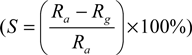
increases with thickness of the sensing film, with a highest sensor response (~67%) observed for 90 nm thin film and thereafter it decreases. The structural and optical properties clearly support the observed enhanced sensor response for 90 nm thin film.