To save content items to your account,
please confirm that you agree to abide by our usage policies.
If this is the first time you use this feature, you will be asked to authorise Cambridge Core to connect with your account.
Find out more about saving content to .
To save content items to your Kindle, first ensure no-reply@cambridge.org
is added to your Approved Personal Document E-mail List under your Personal Document Settings
on the Manage Your Content and Devices page of your Amazon account. Then enter the ‘name’ part
of your Kindle email address below.
Find out more about saving to your Kindle.
Note you can select to save to either the @free.kindle.com or @kindle.com variations.
‘@free.kindle.com’ emails are free but can only be saved to your device when it is connected to wi-fi.
‘@kindle.com’ emails can be delivered even when you are not connected to wi-fi, but note that service fees apply.
Mechanical testing of micro- and nanoscale materials is challenging due to the intricate nature of specimen preparation and handling and the required load and displacement resolution. In addition, in Situ testing requires the entire experimental setup to be drastically miniaturized, because conventional high-resolution microscopes or analytical tools usually have very small chambers. These challenges are increasingly being addressed using microelectromechanical systems (MEMS)-based sensors and actuators. Because of their very small size, MEMS-based experimental setups are the natural choice for materials characterization under virtually all forms of in Situ electron, optical, and probe microscopy. The unique advantage of such in Situ studies is the simultaneous acquisition of qualitative (up to near atomic visualization of microstructures and deformation mechanisms) and quantitative (load, displacement, flaw size) information of fundamental materials behavior. In this article, we provide a state-of-the-art overview of design and fabrication of MEMS-based devices for nanomechanical testing. We also provide a few case studies on thin films, nanowires, and nanotubes, as well as adhesion-friction testing with a focus on in Situ microscopy. We conclude that MEMS devices offer superior choices in handling, actuation, and force and displacement resolutions. Particularly, their tight tolerances and small footprints are difficult to match by off-the-shelf techniques.
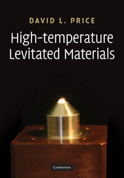
One of the major experimental difficulties in studying materials at extreme temperatures is unwanted contamination of the sample through contact with the container. This can be avoided by suspending the sample through levitation. This technique also makes metastable states of matter accessible, opening up new avenues of scientific enquiry, as well as possible new materials for technological applications. This book describes several methods of levitation, the most important being aerodynamic, electromagnetic and electrostatic. It summarizes the state-of-the-art of the measurement of structural, dynamic and physical properties with levitation techniques, the considerable progress made in this field in the past two decades, and prospects for the future. It also explores the concepts behind the experiments and associated theoretical ideas. Aimed at researchers in physics, physical chemistry and materials science, the book is also of interest to professionals working in high-temperature materials processing and the aerospace industry.
In electronics and photonics, intrinsic properties of semiconducting materials play a dominant role in achieving high-performance devices and circuits. In this respect, carbon nanotubes are prime candidates because of their exceptionally high carrier mobility, low capacitance, and strong optical response (direct bandgap). Although these properties compare very favorably with those of crystalline silicon, several issues related to their synthesis, processing, and assembly have challenged efforts for making electronic and photonic devices. Tremendous progress, nevertheless, has been achieved over the years, and much has been learned from novel photonic devices and electronic circuits. We review some of the developments in nanotube transistor performance optimization, ac operation, nanotube circuits, self-assembly, thin-film devices, and nanotube optical devices such as light emitters and detectors. We also examine the issues and opportunities that still exist.
Layer-structured polypyrrole/montmorillonite (PPy/MMT) naoncomposite films were synthesized by the electrodeposition method. The fabricated free-standing films consist of about 0∼2 wt% Na+-montmorillonite (NMMT). The thickness of films could be controlled by deposition time. X-ray diffraction (XRD) and scanning electron microscope (SEM) were used to observe the microstructure of the films. After MMT was introduced into the PPy matrix, the interspace between PPy chains decreased, according to the XRD results. The layered structure of the films was observed from the SEM images. Tensile and nanoindentation test results showed that the mechanical properties of the composite films were improved at low clay loading. The electrical conductivity of the films with 1.2 wt% MMT loading was increased from 3.6 to 51 S/cm, probably because of the restricted growth of PPy chains in the interspace of MMT layers.
The classical theory of electrolyte solutions starts with the assumption that ionic interactions in solution or between colloid particles are dictated by Coulomb, electrostatic forces alone. An ion is considered to first approximation to have a charge distribution confined to a hard sphere of a given radius. In the ‘primitive’ model the ions are immersed in water (or another solvent) within which they interact by electrostatic interactions. The solvent is treated as a passive dielectric continuum. The radius of an ion is not always just its crystallographic radius. It is an effective radius that includes one or two water layers of ‘hydration’. What occurs in the theory for the free energy of interactions involves the sum of hydrated ion radii besides the Coulomb force. The hydrated ion size is derived as a fitting parameter from comparison of theory with experiments.
For interactions between ions the long-range Coulomb interactions dominate for very dilute solutions below about 5·10−2 M, and ion size is irrelevant. At higher electrolyte concentrations, around and above about 10−1 M, the cooperative electrostatic interactions that dominate at low concentrations become progressively less important. Shorter-range forces subsumed in the ionic ‘radii’ begin to come into play. When short-range interactions between the ions become significant the molecular structure of the water in the immediate neighbourhood of the ions (hydration) becomes a dominant feature. Hydration and local hydrogen bonding are words that attempt to describe this ion-specific, local water structure induced by the ions.
PtPd@Pt core-shell ultrathin nanowires were prepared using a one-step phase-transfer approach. The diameters of the nanowires range from 2 to 3 nm, and their lengths are up to hundreds of nanometers. Line scanning electron energy loss spectra showed that PtPd bimetallic nanowires have a core-shell structure, with a PtPd alloy core and a Pt monolayer shell. X-ray absorption near edge structure (XANES) spectra reveal that a strong Pt-Pd interaction exists in this nanowire system in that there is PtPd alloying and/or interfacial interaction. Extended x-ray absorption fine structures (EXAFS) further confirms the PtPd@Pt core-shell structure. The bimetallic nanowires were determined to be face-centered cubic structures. The long-chain organic molecules of n-dodecyl trimethylammonium bromide and octadecylamine, used as surfactants during synthesis, were clearly observed using aberration-corrected TEM operated at 80 KV. The interaction of Pt and surfactants was also revealed by EXAFS.
Quasicrystals have been identified as alloys possessing unusually low surface energy. This results in poor adhesion properties of quasicrystalline coatings when deposited on metallic substrates, hindering the development of these new materials for technological applications. Here we investigate the possible use of complex Al-Cu metallic phases as interface layers to accommodate the structural and electronic mismatch between a quasicrystalline coating and a metallic substrate and improve adhesion. First, we show that all stable low-temperature phases of the Al-Cu system can be grown as thin films using DC magnetron sputtering. Among the various possible phases, we select the γ-brass γ-Al4Cu9 as a promising candidate for the interface layer. Then the γ-Al4Cu9 phase is grown on the fivefold surface of an icosahedral (i-) Al-Pd-Mn quasicrystal. The interface is investigated by transmission electron microscopy and shows a clear texturing of the film. The grains exhibit rotational epitaxy with the substrate. We find that the interface is mainly composed of a β-phase of unknown chemical composition and sometimes exhibits γ grains in direct contact with the quasicrystalline substrate. Occasionally, we observe a fourth phase at the β/γ interface, identified as β1, possessing a lattice parameter aβ1 equal to 2aβ and 2/3aγ.
Finite element analysis is used to simulate cone indentation creep in materials across a wide range of hardness, strain rate sensitivity, and work-hardening exponent. Modeling reveals that the commonly held assumption of the hardness strain rate sensitivity (mH) equaling the flow stress strain rate sensitivity (mσ) is violated except in low hardness/modulus materials. Another commonly held assumption is that for self-similar indenters the indent area increases in proportion to the (depth)2 during creep. This assumption is also violated. Both violations are readily explained by noting that the proportionality “constants” relating (i) hardness to flow stress and (ii) area to (depth)2 are, in reality, functions of hardness/modulus ratio, which changes during creep. Experiments on silicon, fused silica, bulk metallic glass, and poly methyl methacrylate verify the breakdown of the area-(depth)2 relation, consistent with the theory. A method is provided for estimating area from depth during creep.
Thin-film transistors (TFTs) with zinc oxide channel layers were fabricated through a simple and low-cost solution process. Precursor solution concentration, annealing temperature, and the process were controlled for the purpose of improving the electrical properties of ZnO TFTs and analyzed in terms of microstructural scope. The fabricated ZnO films show preferential orientation of the (002) plane, which contributes to enhanced electron conduction and a dense surface. The results show that the TFT characteristics of the film are clearly affected by the microstructure. The optimized TFT operates in a depletion mode, shows n-type semiconductor behavior, and is highly transparent (>90%) within the visible light range. It exhibits a channel mobility of 9.4 cm2/V·s, a subthreshold slope of 3.3 V/decade, and an on-to-off current ratio greater than 105. In addition, the result of N2 annealing shows the possibility of improvement in electrical property of the ZnO TFTs.
There has been a tireless quest by the designers of micro- and nanoelectro mechanical systems (MEMS/NEMS) to find a suitable material alternative to conventional silicon. This is needed to develop robust, reliable, and long-endurance MEMS/NEMS with capabilities for working under demanding conditions, including harsh environments, high stresses, or with contacting and sliding surfaces. Diamond is one of the most promising candidates for this because of its superior physical, chemical, and tribomechanical properties. Ultrananocrystalline diamond (UNCD) and nanocrystalline diamond (NCD) thin films, the two most studied forms of diamond films in the last decade, have distinct growth processes and nanostructures but complementary properties. This article reviews the fundamental and applied science performed to understand key aspects of UNCD and NCD films, including the nucleation and growth, tribomechanical properties, electronic properties, and applied studies on integration with piezoelectric materials and CMOS technology. Several emerging diamond-based MEMS/NEMS applications, including high-frequency resonators, radio frequency MEMS and photonic switches, and the first commercial diamond MEMS product—monolithic diamond atomic force microscopy probes—are discussed.
An improvement of the fatigue resistance of rolled AZ31 magnesium alloy was attempted by reducing the tensile mean stress developed during fatigue deformation, which was achievable by tailoring the {10-12} twinning-detwinning characteristics of the material through the precompression process. The modification of the {10-12} twinning-detwinning characteristics made it possible to control the plastic deformation mechanisms activated during fatigue deformation so that the imposed tensile strain could be fully accommodated by detwinning alone, which led to a significant reduction of tensile flow stress, finally resulting in the reduction of mean stress.
Molecular forces: some of the background and history of ideas. Why molecular forces?
The matter that concerns us was most clearly articulated nearly a century ago by D'Arcy Thompson in his famous book. He reported the pleas of the early founders of the cell theory, of the then biology, and of the physiologists, that chemists should address the question of molecular forces, then unknown.
We would like to know how it is that molecular forces and the laws of statistical mechanics conspire, with the geometry of molecules and the conformations available to macromolecules, to give rise to the hierarchies of self-assembled equilibrium or dynamic steady states of matter that form cells and dictate biochemical reactivity.
In other words, the game is to link structure and function, the geometry of assemblies of molecules, to the forces that drive self assembly and recognition processes. Any insights ought to allow us to build better, useful connections between the physical and biological sciences. Despite tantalizing hints, that main aim has remained elusive.
D'Arcy Thompson tells us too that of the chemistry of his day and age, Kant said that ‘it was wisschenschaft, nicht Wissenschaft; in that the criterion of a true science lay in its reliance on mathematics’. Kant believed that Euclid's geometry was self-evidently that of nature. We now know better. Hyperbolic geometries that we shall come to later better describe the bicontinuous, random honeycombs of nature.
YB22C2N is one of a series of rare earth borocarbonitrides and is potentially the long awaited n-type counterpart to boron carbide. We conducted studies on YB22C2N spark plasma sintered with additions of YB4 and YB25C, including the investigations of the densification process and the thermoelectric properties of the material. We discovered that a small amount of dopants can lower the starting temperature of densification during spark plasma sintering (SPS). Variations of pressure and temperature during the sintering process are also found to have an effect. Electrical conductivity of the dense samples has increased due to insertion of metal borides and also because of the improvement of the relative density. At the same time, only a slight reduction was observed for the Seebeck coefficient leading to an important improvement of power factor. The highest density of more than 95% was achieved with 5 wt% of YB25(C) dopant.
A new function that describes the shape of three-sided pyramidal indenters is introduced. This function differs from the polynomial tip shape function conventionally used in nanoindentation tip shape calibration in that the new function includes fewer fitting parameters with clearer physical meaning. Specifically, two of the fitting parameters integrated into the new function are the indenter’s tip radius and the slope of the indenter’s equivalent cone. Tip shape calibration data were collected with four different diamond indenter tips, and both the new function and the standard polynomial function were fit to the data. It is found that the new function can fit calibration data nearly as well as the standard polynomial function and better than existing physically based functions. Although the tip radius parameter obtained by fitting the new model to data deviates from the tip radius determined from Hertzian elastic contact, the two values are correlated.