Refine search
Actions for selected content:
106104 results in Materials Science
Suitability of Atmospheric-pressure MOCVD CdTe Solar Cells for Inline Production Scale
-
- Journal:
- MRS Online Proceedings Library Archive / Volume 1165 / 2009
- Published online by Cambridge University Press:
- 31 January 2011, 1165-M07-03
- Print publication:
- 2009
-
- Article
- Export citation
Pad Topography, Contact Area and Hydrodynamic Lubrication in Chemical-Mechanical Polishing
-
- Journal:
- MRS Online Proceedings Library Archive / Volume 1157 / 2009
- Published online by Cambridge University Press:
- 31 January 2011, 1157-E01-02
- Print publication:
- 2009
-
- Article
- Export citation
Comparison of two Metal Ion Implantation Techniques for Fabrication of Gold and Titanium Based Compliant Electrodes on Polydimethylsiloxane
-
- Journal:
- MRS Online Proceedings Library Archive / Volume 1188 / 2009
- Published online by Cambridge University Press:
- 31 January 2011, 1188-LL03-09
- Print publication:
- 2009
-
- Article
- Export citation
Characterization of Ag Nanocrystals for use in Solar Cell Applications
-
- Journal:
- MRS Online Proceedings Library Archive / Volume 1211 / 2009
- Published online by Cambridge University Press:
- 31 January 2011, 1211-R11-37
- Print publication:
- 2009
-
- Article
- Export citation
Spectroscopy Analysis of the Ring Opening Reaction in Functionalized Spiropyran Films
-
- Journal:
- MRS Online Proceedings Library Archive / Volume 1242 / 2009
- Published online by Cambridge University Press:
- 01 February 2011, S4-P68
- Print publication:
- 2009
-
- Article
- Export citation
Plasma Synthesis: A Novel Way of Making Catalysts
-
- Journal:
- MRS Online Proceedings Library Archive / Volume 1209 / 2009
- Published online by Cambridge University Press:
- 31 January 2011, 1209-P03-05
- Print publication:
- 2009
-
- Article
- Export citation
Determination of Thermal Parameters of Nanostructures Exhibiting One-Dimensional Heat Flow Through a Thermal Transient Method
-
- Journal:
- MRS Online Proceedings Library Archive / Volume 1172 / 2009
- Published online by Cambridge University Press:
- 31 January 2011, 1172-T05-05
- Print publication:
- 2009
-
- Article
- Export citation
Microstructure evolution of Ca0.33CoO2 thin films investigated by high-angle annular dark-field scanning transmissionelectron microscopy
-
- Journal:
- Journal of Materials Research / Volume 24 / Issue 1 / January 2009
- Published online by Cambridge University Press:
- 26 July 2012, pp. 279-287
- Print publication:
- January 2009
-
- Article
- Export citation
-
Microstructures of epitaxial Ca0.33CoO2 thin films, which were grown on m
 plane and c(0001) plane of α–Al2O3 by the reactive solid-phase epitaxy (R-SPE) method and the subsequent ion-exchange treatment, were investigated in detail by using selected-area electron diffraction, high-resolution transmission electron microcopy, spherical-aberration-corrected high-angle annular dark-field scanning transmission electron microscopy (Cs-corrected HAADF-STEM), and electron energy-loss spectroscopy (EELS). Detailed electron diffraction analyses reveal that the orientation relationships between Ca0.33CoO2 thin film and substrate are
 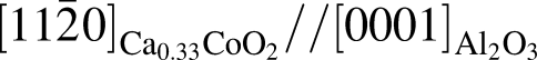 and
and 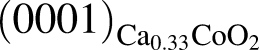 , having an angle of about 43° with
 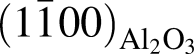 for the film deposited on m
 plane, and
 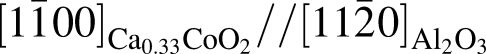 and
and  for the film deposited on c(0001) plane though a Ca–Al–O amorphous layer formed between them. CoO seed layer near the interface and residual Co3O4 phase inside the films were observed and identified by HAADF-STEM and EELS in both samples. Such microstructural configuration indicates that the processes of film growth during R-SPE are (i) oxidation of CoO into Co3O4 with residual CoO layer near the interface and (ii) intercalation of Na+ layer into Co3O4 to achieve the layered NaxCoO2 film while forming Na–Al–O amorphous layer at the interface.
 plane and
  and
and  , having an angle of about 43° with
  for the film deposited on
  plane, and
  and
and  for the film deposited on
 The role of uranium peroxide studtite on the retention of Cs, Sr and Se(VI)
-
- Journal:
- MRS Online Proceedings Library Archive / Volume 1193 / 2009
- Published online by Cambridge University Press:
- 15 February 2011, 621
- Print publication:
- 2009
-
- Article
- Export citation
Fabrication, Characterization and Optical Studies of Cu(In1-xGax)3Se5 Bulk Compounds
-
- Journal:
- MRS Online Proceedings Library Archive / Volume 1210 / 2009
- Published online by Cambridge University Press:
- 31 January 2011, 1210-Q03-14
- Print publication:
- 2009
-
- Article
- Export citation
Implementation of a Curriculum Leading to a Baccalaureate Degree in Nanoscale Science
-
- Journal:
- MRS Online Proceedings Library Archive / Volume 1233 / 2009
- Published online by Cambridge University Press:
- 31 January 2011, 1233-PP09-02
- Print publication:
- 2009
-
- Article
- Export citation
Fidelity of Holographic Lithography for Fabrication of 3D SU-8 Photonic Structures and How to Minimize Distortion by Optical Design
-
- Journal:
- MRS Online Proceedings Library Archive / Volume 1182 / 2009
- Published online by Cambridge University Press:
- 31 January 2011, 1182-EE13-07
- Print publication:
- 2009
-
- Article
- Export citation
Degradation Mechanism of GaN-based LEDs With Different Growth Parameters
-
- Journal:
- MRS Online Proceedings Library Archive / Volume 1195 / 2009
- Published online by Cambridge University Press:
- 31 January 2011, 1195-B08-06
- Print publication:
- 2009
-
- Article
- Export citation
Light Effective Mass in the Widely-Dispersed Valence Band of Single Crystalline Rubrene Observed by High-Resolution Angle-Resolved Ultraviolet Photoelectron Spectroscopy
-
- Journal:
- MRS Online Proceedings Library Archive / Volume 1197 / 2009
- Published online by Cambridge University Press:
- 31 January 2011, 1197-D07-31
- Print publication:
- 2009
-
- Article
- Export citation
Investigation of Characteristics of Multi-Function ZnO Thin Film Deposited with Various Argon and Oxygen Ratios
-
- Journal:
- MRS Online Proceedings Library Archive / Volume 1174 / 2009
- Published online by Cambridge University Press:
- 31 January 2011, 1174-V09-05
- Print publication:
- 2009
-
- Article
- Export citation
Biosensor Capture Kinetics Model of Nanocube-Augmented Carbon Nanotube Networks
-
- Journal:
- MRS Online Proceedings Library Archive / Volume 1236 / 2009
- Published online by Cambridge University Press:
- 31 January 2011, 1236-SS05-07
- Print publication:
- 2009
-
- Article
- Export citation
Layer-by-Layer Assembly of Nanotube-Polymer Thin Films with High Electrical Conductivity and Transparency
-
- Journal:
- MRS Online Proceedings Library Archive / Volume 1205 / 2009
- Published online by Cambridge University Press:
- 31 January 2011, 1205-L08-03
- Print publication:
- 2009
-
- Article
- Export citation
Development of Diamond-Based X-ray Detection for High Flux Beamline Diagnostics
-
- Journal:
- MRS Online Proceedings Library Archive / Volume 1203 / 2009
- Published online by Cambridge University Press:
- 31 January 2011, 1203-J19-03
- Print publication:
- 2009
-
- Article
- Export citation
Silicon Nitride Membrane Dynamic Masking Allows Improved Shapes of Near-Field Optical Apertures Fabricated by FIB
-
- Journal:
- MRS Bulletin / Volume 34 / Issue 1 / January 2009
- Published online by Cambridge University Press:
- 31 January 2011, pp. 5-6
- Print publication:
- January 2009
-
- Article
-
- You have access
- Export citation
Electrochemical Deposition of Apatite/Collagen Composite Coating on NiTi Shape Memory Alloy and Coating Properties
-
- Journal:
- MRS Online Proceedings Library Archive / Volume 1239 / 2009
- Published online by Cambridge University Press:
- 31 January 2011, 1239-VV02-07
- Print publication:
- 2009
-
- Article
- Export citation
