To save content items to your account,
please confirm that you agree to abide by our usage policies.
If this is the first time you use this feature, you will be asked to authorise Cambridge Core to connect with your account.
Find out more about saving content to .
To save content items to your Kindle, first ensure no-reply@cambridge.org
is added to your Approved Personal Document E-mail List under your Personal Document Settings
on the Manage Your Content and Devices page of your Amazon account. Then enter the ‘name’ part
of your Kindle email address below.
Find out more about saving to your Kindle.
Note you can select to save to either the @free.kindle.com or @kindle.com variations.
‘@free.kindle.com’ emails are free but can only be saved to your device when it is connected to wi-fi.
‘@kindle.com’ emails can be delivered even when you are not connected to wi-fi, but note that service fees apply.
Flowerlike ZnO nanoneedle arrays have been synthesized on Si (100) substrates by pulsed laser deposition techniques. The tips of the nanoneedles are ˜ 20- 50 nm in diameter and their roots are as thick as ˜ 50- 100 nm. The nanoneedle arrays grow preferentially along the [0001] direction. Raman spectroscopy shows three first order optical normal modes which confirm wurtzite structure of ZnO nanoneedles. In the low frequency zone, additive modes (92, 122, 163, and 275 cm-1) are observed and can be attributed to zone boundary phonons. ZnO nanoneedle arrays exhibit a strong UV luminescence emission, and two strong peaks at 3.258 eV and 3.288 eV are observed.
This paper investigates the sound absorption characteristics of porous steel samples manufactured by Lost Carbonate Sintering. Measurements of the normal incidence sound absorption coefficient were made using an impedance tube for single-layer porous steel discs and assemblies comprising four layers of porous steel discs. The sound absorption coefficient was found not to vary significantly with pore size in the range of 250-1500 μm. In general, the absorption coefficient increases with increasing frequency and increasing thickness, and peaks at specific frequencies depending on the porosity. An increase in porosity tends to increase the frequency at which the sound absorption coefficient reaches this peak. An advantage was found in using an assembly of samples with gradient porosities of 75%-70%-65%-60% as it gave higher and more uniform sound absorption coefficients than an assembly with porosities of 75%.
The etch rate and surface morphology of Zn-containing oxide and HfO2 films after wet chemical etching were investigated. ZnO could be easily etched using each acid tested in this study, specifically sulfuric, formic, oxalic, and HF acids. The etch rate of IGZO was strongly dependent on the etchant used, and the highest measured etch rate (500 nm/min) was achieved using buffered oxide etchant at room temperature. The etch rate of IGZO was drastically increased when sulfuric acid at concentration greater than 1.5 molar was used. Furthermore, etching of HfO2 films by BF acid proceeded through lateral widening and merging of the initial irregular pits.
Rapidly evolving plasmas represent a challenging environment for both study and control. Density, collision frequency and temperature fluctuations can change over orders of magnitude on time scales of one ns with spatial features less than one cm and thus are not amenable to conventional continuous-wave diagnostic techniques such as microwave or mm-wave interferometry. We have developed a new technique for studying plasmas undergoing rapid nonequilibrium changes that uses THz time-domain spectroscopy (THz-TDS) in conjunction with optical fluorescence imaging. The advantages of using THz pulses lie in the fact that the broad bandwidth of a THz pulse contains frequency components both above and below the plasma frequency allowing a single ps-duration pulse to carry away information about the complex path-integrated susceptibility. Transverse fluorescence gives us a model of the longitudinal plasma distribution and using a novel rms error-minimization technique we can recover the real and imaginary parts of the susceptibility with <5 mm spatial and, potentially, ps time resolution (we are currently limited by S/N considerations to averaging over several THz pulses and thus obtain 40 ns resolution). From this we obtain the electron density and collision frequency, spatially and temporally resolved, with dynamic range >103. The principle of this new technique will be discussed along with results on a pulsed DC-discharge plasma. We will also present some new ideas such as concurrent molecular spectroscopy and computed tomography.
ZnO nanostructures were grown by pulsed laser deposition on c-plane sapphire substrates. The as-grown nanostructures were examined by scanning electron microscopy and transmission electron microscopy ZnO nanowires were grown using a gold catalyst, at a high substrate temperature of 800°C and an ambient gas pressure of 0.5 mbar (5% oxygen, 95% argon). Changing the gas composition to pure oxygen led to the growth of stacking fault-free ZnO nanosheets with their growth direction inclined to the [0001] direction. Similar nanosheets with stacking faults were found when lowering the growth temperature to 600°C for a 5% oxygen – 95% argon ambient gas composition and the same overall pressure. A growth mechanism for these ZnO nanosheets is proposed.
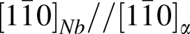
The orientation relationship (OR) and the interfacial structure between Nb solid solution (Nbss) precipitates and α-Nb5Si3 intermetallics have been investigated by transmission electron microscopy (TEM). The OR between Nbss and α-Nb5Si3 was determined by selected-area electron diffraction analyses as (222)Nb//(002)α and . High-resolution TEM images of the Nbss/α-Nb5Si3 interface were presented. Steps existed at the interface that acted as centers of stress concentration and released the distortion of lattices to decrease the interfacial energy. In addition, the interfacial models were proposed based on the observed OR to describe the atomic matching of the interface. The distribution of alloying elements at the Nbss/α-Nb5Si3 interface has also been investigated, and Hf was enriched at the interface to strengthen the grain boundary.
We report the systematic substitution of Nb at the Cu1 site of YBa2Cu3Oy in thin films to form a new phase of YBa2Cu2NbO8. These films were deposited on SrTiO3(100) crystals using pulsed laser deposition and deposited at an optimal temperature of 850 °C. Films were characterized using x-ray diffraction (XRD), atomic force microscopy, x-ray photoelectron spectroscopy (XPS), micro-Raman spectroscopy, and transmission electron microscopy. XRD of these films indicate c-axis oriented YBa2Cu2NbOy formation. XPS and micro-Raman spectroscopy analysis suggests Cu exists in the +2 state.
Composite aerogels (with varying concentrations of silica and poly-dimethylsiloxane) were developed and their acoustic absorption coefficient as a function of composition and average pores size have been measured. The polydimethylsiloxane modified the ceramic structure of the silica aerogels, decreasing the material’s rigidity while maintaining the high porosity of the aerogel structure. The composite aerogels were found to exhibit different modesof acoustic absorption than that of typical porous absorbers such as fiberglass. At some frequencies, the composite aerogels had 40% higher absorption than that of commercial fiberglass. Physical data show that these materials have a large surface area (> 400 m2/g) and varying pore sizes (d ˜ 5 - 20 nm).
We have simulated the angle-dependent absorption and thermal emittance of two dimensional metallic and metallodielectric photonic crystals (PCs) with rigorous scattering matrix methods- where Maxwell's equations are solved in Fourier space. These metallic photonic crystals exhibit strong thermal emittance and absorption peaks in the normal direction. This peak splits into multiple peaks at larger and shorter wavelengths away from the normal direction. The thermal emission at different wavelengths is redistributed into different emission angles. There is partial suppression of photon emission at long wavelengths and enhancement at the shorter wavelength spectral range where the thermal emittance has a maximum. Angle-dependent measurements of the emission in metallo-dielectric photonic crystals are performed. Simulations compare well with these measurements and are consistent with the surface plasmon model. The strong dependence of the absorption with angle is very important for thermo-photovoltaic devices.
We present an efficient polymer-small molecule triple-tandem organic solar cell (OSC), consisting of poly(3-hexylthiophene) (P3HT) and 1-(3-methoxycarbonyl)-propyl-1-phenyl-(6,6)C61 (PCBM) bulk heterojunction as the first and second cells, and small molecules copper phthalocyanine (CuPc) and fullerene (C60) as the third cell on top. These sub-cells are connected by an intermediate layer of Al(1 nm)/MoO3(15 nm), which appears to be highly transparent, structurally smooth, and electrically functional. Compared to our previous all polymer triple-tandem organic solar cells (2.03%), this polymer-small molecule triple-tandem organic solar cell achieves an improved power conversion efficiency of 2.18% with a short-circuit current density (Jsc) = 3.02 mA/cm2, open-circuit voltage (Voc) = 1.51 V, and fill factor (FF) = 47.7% under simulated solar irradiation of 100 mW/cm2 (AM1.5G), which can be attributed to the increased photocurrent generation in the third cell since the third cell has the complementary absorption with two bottom cells despite a slightly reduced Voc.
Current-voltage (I-V) characteristic of Pt/TiO2-x/Pt has been investigated. The Pt/TiO2-x/Pt devices in the initial state exhibit a rectifying I-V behavior. By applying a pulse voltage, the rectifying polarity could be switched to an opposite direction. The mechanism of the rectifying polarity switch is proposed as the local drift of defects, such as oxygen vacancies (VO), due to applying pulse voltage. It is found that the required pulse voltage height for the polarity switch (Vswitch) exhibits much dependence on the operation temperature and width of applied pulse voltage. With an increase of the pulse voltage width or the measurement temperature (T), Vswitch exhibits a decrease with increase of T. These results suggest that the rectifying polarity switch in the Pt/TiO2-x/Pt is attributed to a thermal and dynamic dependence process, which agree well with the localized migration of VO induced by applied pulse voltage.
High electron mobility transistors (HEMTs) based on AlGaN-GaN hetero-structures are promising for high power, high speed, and high temperature operation. Especially, AlGaN-GaN HEMTs grown on semi-insulating (SI) SiC substrates are the most promising for both military and commercial applications. High performance characteristics from these devices are possible in part due to the presence of high two-dimensional electron gas charge sheet density maintaining a high Hall mobility at the AlGaN barrier-GaN buffer hetero-interface and in part due to high thermal conductivity of the SiC substrates. However, long-term reliability of these devices still remains a major concern because of the large number of traps and defects present both in the bulk as well as at the surface leading to undesirable characteristics including current collapse. We report on the study of traps and defects in two MOCVD-grown structures: Al0.27Ga0.73N HEMTs on SI SiC substrates and Al0.27Ga0.73N Schottky diodes on conducting SiC substrates. Our HEMT structures consisting of undoped AlGaN barrier and GaN buffer layers grown on an AlN nucleation layer show a charge sheet density of ∼1013/cm2 and a Hall mobility of ∼1500cm2/V·sec. Deep level transient spectroscopy (DLTS) was employed to study traps in AlGaN Schottky diodes and HEMTs fabricated with different Schottky contacts consisting of Pt/Au and Ni/Au. Focused ion beam was employed to prepare both cross-sectional and plan view TEM samples for defect analysis using a high resolution TEM.
By launching new processes introduced by nano science into much more conventional industrial applications fast, robust and economical reasonable inspection methods are required for process control and quality assurance. Coming from high tech industries e.g. semiconductor industries the methods available for thin film characterization and quality control are complex and often require scientific skilled personal. High frequency eddy current spectroscopy in reflection or transmission configuration allows a contactless measurement of e.g. copper thin films on silicon with a thickness resolution better that 5 nm. Due to the insensitivity of the transmission mode to dislocations or slight tilting of the sample the high frequency eddy current method is a practicable method for thin film characterization under industrial environment.
We provide a brief discussion of the Boltzmann equation derived Callaway-Debye relaxation time theory of lattice thermal conductivity of micro- and nano-structured materials (of size greater than 20 nm. Incorporated in the theory is a comprehensive treatment of three-phonon scattering events. Using numerical results from this theory, we present a quantitative investigation of the magnitude and temperature variation of the conductivity of CVD polycrystalline diamond films, suspended GaAs nanostructures, Si nanowires, and AlN micro- and nano-ceramics.
We show results of in situ TEM (Transmission electron microscope) quantitative investigations on the compression behaviors of amorphous micropillars fabricated by focused ion beam from Cu47Ti33Zr11Ni6Sn2Si1 metallic glass (MG) ribbon. Pillars with well defined gauge sections and tip diameter ranging from 100 nm to 640 nm are studied. Quantitative compression tests were performed by a recently developed Picoindenter TEM holder, with the evolution of individual shear bands monitored in real time in TEM. It is found that the deformation of the MG pillars at the present size domain is still dominated by discrete shear banding as demonstrated by intermittent events in the load-displacement curves. However, the frequency, amplitude and distribution of these shear banding events are clearly size dependent at submicrometer scale, leading to an apparently transition in deformation mode from highly localized inhomogeneous deformation to less localized and more distributed deformation with decreasing pillars diameter. Deformation of a 105 nm diameter pillar having rounded tips is characterized with fully homogeneous bulge at the initial stage of deformation, indicating prompting effect of multi-axial stress state on transition to fully homogeneous deformation.
Clay aerogel composites have been around for over 50 years but still they represent a relatively under studied class of materials. Clay aerogel composites have been made in our labs that have low densities, 0.05-0.1g/cm3, provide good thermal insulation, k 0.02W/mK, and are created through an environmentally benign process. The mechanical properties of the composites resemble those of typical foamed polymers such as expanded polystyrene and polyurethane, with compressive moduli ranging from 0.5MPa to 40MPa depending on composition. Aqueous solutions of clay and polymer are frozen in cylindrical molds and freezedried to create these foam-like materials. Typically there is no particular orientation to the often layered structure that results, however if frozen in a unidirectional manner, anisotropic materials can be made. In this paper we will discuss the effects of molecular weight on mechanical properties of various composites as well as discussing the orientated layered structure within the anisotropic materials.
We present x-ray diffraction based methods to quantitatively determine the wurtzite content of nanowire ensembles and to investigate the effect of twinning. An increased lattice constant in growth direction is found for all investigated InAs and InP nanowire samples. This increase is independent of the wurtzite content. Using x-ray pole figures we find that twinning is present in GaAs/Si branched nanowires, which leads to 60° rotations of the lattice.
We have investigated the Pb depletion in laser ablated PZT (PbZr0.52Ti0.48O3) films through a systematic study of PZT target-laser interactions for both single laser and dual-laser ablation methods. The study includes films deposited from a stoichiometric and an excess PbO PZT targets. The films were deposited on single crystal SrTiO3[100] substrates at 550˚C with a background oxygen pressure of 500 mT. Single laser deposited films at a laser fluence of 5J/cm2 produced the highest Pb content while dual-laser ablated films where an excimer and a CO2 pulsed lasers were synchronized for ablation produced high Pb content for an excimer laser fluence of less than 2J/cm2. This enabled the growth of particulate-free PZT films with high Pb content. ICCD imaging of the plasma plumes showed variations in the expansion profiles at different laser fluencies that correlated well with the Pb content observed in the deposited films.
Nanoparticles (NPs) are being used extensively for tumor drug delivery. These devices offer the advantage of their size, protection of the encapsulated species, and biodegradability to prevent accumulation in the interstitium. Our laboratory has synthesized polylactide fumarate (PLAF, PLGF) macromers capable of self-assembling into biodegradable and biocompatible NPs with average particle size of 280 nm. To assess the possibility of further decreasing the particle size and distribution of PLGF NPs, the polymers were conjugated with the peptide sequence Cys-Val-Val-Val-Val-Val-Val-Lys-Lys (CV6K2), which is known to self-assemble in aqueous solution into vesicles of about 50-60 nm in size. The results indicate that the PLGF-CV6K2 conjugates are capable of self-assembling into NPs of 100 nm in diameter. The NPs are proposed as having a bilayer structure, with peptide chains facing the aqueous environment and the polymer chains compacted in an internal hydrophobic layer. Degradation kinetics and release profiles show that the NPs could effectively retain and release Paclitaxel up to 30 days until completely degraded. The NPs act as reservoirs for sustained release of the active agent by diffusion and degradation of the matrix when taken up by tumor cells.
We report on the measurement of the thermal conductivity of Si/Si0.8Ge0.2 multilayers on Si substrates through a variation of the 3? method. We exploit the frequency dependent variation of the thermal wave, through invoking the thermal penetration depth (TPD), which is inversely proportional to the frequency. Consequently, spectral measurements covering decades of frequency were used to finely probe the substrate and the overlying Si and Si0.8Ge0.2 thin film layers. Both in-phase and out-of phase measurements yielded comparable values of the thermal conductivity in the range of 3-5 W/mK, much lower than the reported bulk values. Our results provide proof of the potential of multilayered media to be used for reduced thermal conductance applications such as thermoelectrics, heat insulation etc.