To save content items to your account,
please confirm that you agree to abide by our usage policies.
If this is the first time you use this feature, you will be asked to authorise Cambridge Core to connect with your account.
Find out more about saving content to .
To save content items to your Kindle, first ensure no-reply@cambridge.org
is added to your Approved Personal Document E-mail List under your Personal Document Settings
on the Manage Your Content and Devices page of your Amazon account. Then enter the ‘name’ part
of your Kindle email address below.
Find out more about saving to your Kindle.
Note you can select to save to either the @free.kindle.com or @kindle.com variations.
‘@free.kindle.com’ emails are free but can only be saved to your device when it is connected to wi-fi.
‘@kindle.com’ emails can be delivered even when you are not connected to wi-fi, but note that service fees apply.
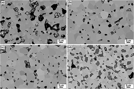
Fe-50 wt% Co alloy powders with average particle size of 10 μm were compacted by spark plasma sintering (SPS) at 700, 800, 900 and 950oC by applying 40, 80, 100 MPa uniaxial pressures for 2, 5, 10 minutes. The densities of the samples were found to increase with temperature from 700 to 900oC for constant sintering pressure and time and to decrease for the material sintered at 950oC. The effects of sintering time on density were more significant in samples sintered at 700oC and 800oC than those densified at 900oC. The consequences of small increases in mechanical pressure during sintering on density values were significant for samples sintered at 700oC. The coercivity (Hc) of the compacts decreased significantly with increasing sintering temperature, and with increasing dwell time at sintering temperatures lower than 700oC. The sample sintered at 950oC, which contains the largest grains among the prepared samples and porous microstructure, exhibited the minimum coercivity. Unlike Hc, the remanence (Br) and saturation induction (Bsat) values were more strongly affected by the specimen density than by grain size. Br and Bsat values were found to vary linearly with sintering temperature and pressure owing to increasing density. An increase in soaking time at 800 and 900 oC, although enabling higher density, exhibited contradicting effects on Bsat values. The SPS parameters to obtain maximum density and optimum magnetic properties for Fe-50% Co alloy were found to be 900oC, 80 MPa and 2-5 minutes.
We report formation of thin aluminum oxide AlOx films on the silicon surface by a simple method of Al metal evaporation in oxygen gas atmosphere. 520 μm thick 30-Ωcm p-type-silicon substrates with a top bare surface and a rear surface coated with 100 nm thick thermally grown SiO2 layers were prepared. AlOx films were formed on the top surfaces by Al metal evaporation up to 20 s in oxygen gas atmosphere at 0.8 Pa with a flow rate of 3 sccm. Samples were subsequently annealed with 9.0x10⁵ Pa H2O vapor at 260°C for 3 h. Measurement of capacitance response to a modulation voltage at 500 kHz as a function of bias gate voltages C-V revealed that AlOx films had the effective oxide thickness ranging from 2.0 and 2.6 nm were formed. C-V measurements also revealed that negative fixed charges were accumulated with a density of 5x1012 cm-2 in AlOx films. Photo-induced carrier microwave absorption measurement resulted in a high minority carrier effective lifetime τeff of 3.6x10⁻⁴ s comparable to that of 4.1x10⁻⁴ s for thermally grown SiO2 passivation. Field effect passivation was probably caused by negative charges in AlOx so that the surface recombination velocity decreased to 70 cm/s. X-ray reflectivity analysis indicated that the interfacial layer like SiOx was formed between AlOx and Si substrate. High pressure H2O vapor heat annealing caused increase in the density and decrease in the thickness of AlOx layers, although it increased the density and thickness of the interfacial SiOx layer thickness. H2O vapor treatment is effective to improve the quality of nanometer thick AlOxlayer.
The electrical conduction mechanism contributing to the leakage current at different field regions has been studied in this work. The current-voltage (I-V) measurement of TiN/HfO2/SiO2/P-Si nMOS capacitor has been taken for two different interfacial layer (SiO2) growth conditions such as in situ steam grown (ISSG) and chemical processes. It is observed that Poole-Frenkel mechanism is the dominant conduction mechanism in high field region whereas Ohmic conduction is dominant in the low field region. Also it is seen that the gate leakage current is reduced for the devices having chemically grown interfacial layer compared to that of ISSG devices. Both trap energy level (ϕt) and activation energy (Ea) increase in the chemically grown interfacial layer devices for the Poole-Frenkel and Ohmic conduction mechanisms respectively in comparison to ISSG devices. Trap energy level (ϕt) of ~ 0.2 eV, obtained from Poole-Frenkel mechanism indicates that the doubly ionized oxygen vacancies (V2-) are the active defects and are contributing to the leakage current in these devices.
High dielectric tunability, low dielectric loss tangent and appropriate level of dielectric constant are the basic requirements for applications as electrically tunable dielectric microwave devices. In our experiments, the SrTiO3 green compacts made of the powder mixtures with various particle sizes were infiltrated with a BaTiO3 precursor solution and sintered at different temperatures between 1280 and 1350 ºC for 2 hours and 1350 ºC for 6 hours. The sintering, microstructural and dielectric properties were investigated. Results showed that the relative density of SrTiO3 ceramics could reached 93% when sintered at 1280 ºC for 2 hours. When sintered for 6 hours at 1350 °C, the room temperature dielectric constant of SrTiO3 reaches 900 at a frequency of 1MHz. It has only weak temperature dependence between 100 and 500K. The reason of the low sintering temperature for the dense SrTiO3 ceramics and the effects of sintering scheme on the dielectric properties from 100 K to 500 K are discussed in this paper.
The nanoscale physical properties of newly electrospun polyamide nanofibrillar matrices < 1 year old versus those that were > 3 year old were investigated with transmission electron microscopy, selected area electron diffraction, contact angle measurements, and Raman spectroscopy. Significant differences in crystallinity, hydrophobicity, and chemistry were found and correspondingly different cell responses by cerebellar granular neurons were observed. The properties of the aged nanofibrillar scaffolds evoked a response for neuron burrowing into a more 3-dimensional environment in addition to better facilitation of neurite outgrowth. The nanophysical properties of tissue scaffolds have been recently shown to directly and indirectly regulate cellular responses. As physical properties can evolve over time, the present investigation addresses the issue of tissue scaffold shelf life, with possible changes in directive signals to cells.
We present a model for organic bistable devices (OBDs) embedded with metallic nanoparticles. In particular, two device architectures have been studied: a single layer device with metallic nanoparticles dispersed in a organic material matrix and a three layer device where two organic material regions are separated by a layer of heavy packed nanoparticles. The model describes the different behavior, the internal charge and potential distributions in the ON-OFF states. The OFF state is represented by charged nanoparticles forming a space charge layer which limits the current. The ON state occurs with neutral nanoparticles.
In this paper, we studied the optimization of preparation for polymeric optical waveguide based bus structures with embedded 45 degree micro-mirrors by metallic hard mold method. The 45º facets on the metallic hard mold, which were used to create the 45 degree micro-mirrors, were studied by the atomic force microscopy (AFM). The surface roughness of the 45 degree facets was reduced from 70nm to be 2nm by a photopolymer coating step. High speed test on the waveguide shows the low loss and high Q-factor performance of the waveguide structures. A backplane bus with 10 Gbits/sec channel will be reported.
The effect of silver nanoparticles showing localised plasmonic resonances on the efficiency of thin film silicon solar cells is studied. Silver (Ag) nanodiscs were deposited on the surface of silicon cells grown on highly doped silicon substrates, through hole-mask colloidal lithography, which is a low-cost and bottom-up technique. The cells have no back reflector in order to exclusively study the effect of the front surface on their properties. Cells with nanoparticles were compared with both bare silicon cells and cells with an antireflection coating. We optically observe a resonance showing an absorption increase controllable by the disc radius. We also see an increase in efficiency with respect to bare cells, but we see a decrease in efficiency with respect to cells with an antireflection coating due to losses at wavelengths below the plasmon resonance. As the material properties are not notably affected by the particles deposition, the loss mechanism is an important absorption in the nanoparticles. We confirm this by numerical simulations.
This work study the effect on aging thermal treatment on micro-alloyed steels API X70 pipe, microstructure and mechanical properties such a yield strength (Y), hardness (Hv) and Young´s modulus (E) are presented in this work. Thermal treatment consists of two phases: i) The solution treatment introducing samples in a electric induction furnace at 1100 °C for 30 min under argon atmosphere and water quenching, ii) aging process for five temperature in the range between 204 to 650 °C for 30 min of time exposition and water quenching, respectively. The microstructural characterization was examined by optical microscopy and matrix samples aging showed microstructures like acicular ferritic, polygonal ferritic and bainitic-ferritic, and the secondary phases were examined by scanning electron microscopy (SEM) and energy dispersive spectroscopy (EDS) obtained by SEM evidencing the presence of precipitates composed of vanadium (V), niobium (Nb) and titanium (Ti). The mechanical properties were evaluated by depth sensitive indentation test at the samples aging, the results showed increase of the (Hv) and (E)to the conditions of low temperature aging.
Convenient preparation of nano/micro scale topography is crucial for the fabrication of low-cost biodevices, which could be useful tools for understanding cell biology mechanisms and for the development of scaffolds for tissue engineering. Such intelligent surfaces have been conventionally fabricated through photolithography, micro-contact printing, and nano/micro imprinting. However, considering the process integration, these approaches are not always adequate in order to produce large dimensional patterns in a convenient and rapid way. In this study, we focused on the convenient fabrication of nano-wrinkles based on the elastic instability between a shape memory polymer sheet and a conductive polymeric film, on which the behavior of murine skeletal muscle cells (C2C12) was evaluated. A tens-of-nm-thick layer of poly(3,4-ethylenedioxythiophene) with poly(styrenesulfonate) (PEDOT:PSS) was spincoated on a thermo-retractable polymer sheet. Then, thermal treatment produced different periodicity of the unidirectional nano-wrinkles on the polymer sheet covered with different thickness of PEDOT:PSS layer. Finally, adhesion and proliferation of C2C12 were evaluated, comparing different samples. The cells preferentially adhered and anisotropically aligned on low and narrow ridges (1.5 μm height) rather than on high and wide ones (2.5 μm height). Furthermore, we observed that these trends were confirmed in the differentiation stage of C2C12 into myotubes. The combination of living cells and tunable nano-wrinkles made of conductive polymeric materials will represent a unique tool for the development of innovative biomedical devices.
Despite the many superior attributes of diamond, electronic device performance to date has fallen well behind theoretical expectation. The potential realization of highly efficient electronic polycrystalline diamond devices has been more than limited by certain technological challenges such as maintaining efficient/shallow n-type doping without higher density of defects or incorporation of sp2 bonded carbon as a result of doping(during ion implantation process). Specific n-type diamond reports demonstrating phosphorus doping (with activation energy reported in the range of 485 meV to 600 meV in (100) oriented systems have been particularly problematic as a lower solubility is found as compared to (111) oriented synthesis efforts, in addition to the reported self-compensating nature. Amongst the previous reports of Phosphorus-doped diamond nearly all experimental reports to date show visual crystallographic dislocation/pitting on the (100) facet with even moderate doping where dislocations have been observed to be incorporated into the bulk volume during growth. These dislocations, which are known carrier scattering sites, subsequently lower mobility rendering poor conductance and high resistivity. Due to this well-known sensitivity of phosphorus incorporation to the crystal quality, typically lower in polycrystalline than homoepitaxial films, polycrystalline-based experimental reports have been largely absent. With respect to Phosphorus in-situ doping based efforts, rendered films demonstrate both the visually identifiable pitting and electronically identifiable poor conduction characteristic, and with respect to ion beam doping efforts, complete graphitic flaking at even moderate doses (i.e. greater than 3x1017cm−3). Motivated by these shortcomings and the success of recent experimentation, we present the methodology and data from our recent successful fabrication of polycrystalline diamond P+-i-N junction (diode) with high crystal quality, high power handling capability, high current density, low threshold voltage, and ohmic contact, under room temperature operation, previously undemonstrated across all diamond material types. The superior electrical performance of the device was obtained by novel ion beam methodology designed to resolve previously unaddressed issues relating to n-type doping of diamond materials. A high current density of approximately 104 A/cm2 is attained at 20V forward bias.
Spatial fluctuations of the microstructure suggest possible self-organized criticality in the Portevin–Le Chatelier plastic instability occurring in age-hardenable alloys. The discontinuous yielding found in a supersaturated Al alloy can be characterized by a universal power-law spectrum that is independent of the experimental conditions. The result provides an explanation for the formation of unexpected detrimental strain localizations when samples are severely deformed, giving a framework for studying the simultaneous effects of solute atoms and precipitates in the decomposition of solid solutions.
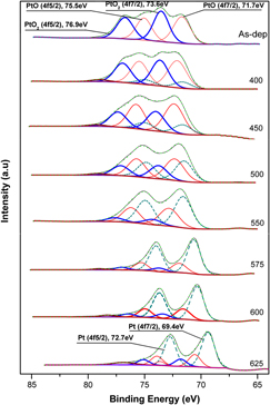
Porous platinum thin films were prepared by thermal decomposition at temperatures from 25 to 675 °C of platinum oxide films deposited by a pulsed reactive sputtering technique. The samples’ chemistry and structure were investigated by x-ray diffraction (XRD), x-ray photoelectron spectroscopy (XPS), and x-ray absorption near edge structure (XANES), showing that the decomposition of the oxide begins as low as 400 °C and follows a sigmoidal trend with increasing annealing temperature. In the XRD spectra, only an amorphous-like signature was observed for temperatures below 575 °C, while Pt 4f XPS showed that the deposited oxide was a mixture of PtO2 and PtO. Pt-L3 edge XANES and Pt 4f XPS spectra showed that the Pt concentration and electronic structure are predominant for temperatures equal to or above 575 °C. The morphologies of the films were investigated by the area-perimeter method from atomic force microscopy and scanning electron microscopy (SEM) images, indicating that the surfaces exhibit a combination of Euclidian and fractal characteristics. Moreover, the thermal evolution of these characteristics indicates the agglomeration of the grains in the film as observed by SEM.
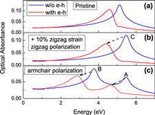
We use the first-principles GW + Bethe–Salpeter equation approach to study the electronic structure and optical absorption spectra of uniaxial strained graphene. Applied strain induces an anisotropic Fermi velocity and tilts the axis of the Dirac cone. As a result, the optical response of strained graphene is dramatically changed; the optical absorption is anisotropic; the characteristic single optical absorption peak of pristine graphene is split into two peaks with enhanced excitonic effects. Within the infrared regime, the optical absorbance of uniaxial strained graphene is no longer a constant because of the broken symmetry and anisotropic excitonic effects. Within the visible-light regime, we observe a prominent optical absorption peak due to an enhanced red shift by electron–hole interactions, enabling us to change the visible color and transparency of stretched graphene. Finally, we also reveal enhanced excitonic effects within the ultraviolet regime, where a few nearly bound excitons are identified.
Bulk ceramics In2−xGexO3 have been synthesized in air by using citrate gel process. Nanoparticles of less than 20 nm have been synthesized through an accurate control of the processing parameters. X-ray diffraction and scanning electron microscopy studies confirmed that the solubility limit of Ge in In2O3 (xℓ) is very small and that additions of more than about 0.5 at.% Ge lead to the presence of In2Ge2O7 inclusions. Thanks to a high interdispersion of metal ions and homogeneity in elemental composition of the nanopowders obtained by citrate gel process, well-dispersed In2Ge2O7 secondary phases can be formed in the Ge-doped In2O3 matrix. An abrupt increase in the electrical conductivity and in the carrier concentration with x is observed in the monophasic region (x < xℓ), whereas in the biphasic region (x > xℓ), these values do not vary significantly. Similarly, the thermopower |S| value is correlated to this variation decreasing as x increases for x < xℓ. Above the solubility limit, the decrease in the lattice thermal conductivity is shown to be dependent on the presence of well-dispersed In2Ge207 secondary phases. The dimensionless figure of merit value is increased up to 0.3, thanks to electron doping and phonon scattering.
The Bosch process is a high-speed, deep reactive ion etching technology for silicon, which has both excellent flexibility and selectivity. For better understanding and control of the time evolution of the feature profile during the Bosch process, an accurate, predictive, and fast simulation tool would be useful. In this article, a simplified model for three-dimensional simulation of the Bosch process is proposed. Etching is modeled by an isotropic etching rate superposed by an anisotropic term. For the passivation cycle, a perfect conformal deposition is assumed corresponding to a constant deposition rate. Level set method was used for tracking the surface evolution. Since the etching and deposition rates are the model input parameters which are not computed, the computational time is significantly reduced. Calculation results presented here illustrate some typical applications of the Bosch process.
Two kinds of type-II heterostructures (HSs) of ZnO (wurtzite)/ZnSe (wurtzite) [ZnO (WZ)/ZnSe (WZ)] and ZnO (wurtzite)/ZnSe (zinc blende) [ZnO (WZ)/ZnSe (ZB)] were designed for photovoltaic applications by first-principle calculations. The calculated effective bandgap of 1.51 eV for the ZnO (WZ)/ZnSe (WZ) HS is more favorable for solar cell applications compared to that of 1.69 eV for the ZnO (WZ)/ZnSe (ZB) HS. Furthermore, the electrons and holes are more effectively separated at the interface of ZnO (WZ)/ZnSe (WZ) HS due to the stronger misfit stress field. Finally, a strained ZB ZnSe layer was introduced to transport the separated holes from WZ ZnSe layer, and an optimal structure of ZnO (WZ)/ZnSe (WZ)/ZnSe (ZB) was proposed to realize a solar cell with near-infrared response.