Refine search
Actions for selected content:
106095 results in Materials Science
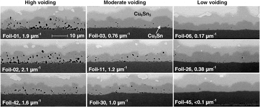
On the root cause of Kirkendall voiding in Cu3Sn
-
- Journal:
- Journal of Materials Research / Volume 26 / Issue 3 / 14 February 2011
- Published online by Cambridge University Press:
- 04 February 2011, pp. 455-466
- Print publication:
- 14 February 2011
-
- Article
- Export citation
Computational Thermodynamics
- The Calphad Method
-
- Published online:
- 03 February 2011
- Print publication:
- 12 July 2007
Nano Focus: High-yield, low-cost approach developed to functionalize MWCNT surface
-
- Journal:
- MRS Bulletin / Volume 36 / Issue 2 / February 2011
- Published online by Cambridge University Press:
- 18 February 2011, p. 86
- Print publication:
- February 2011
-
- Article
-
- You have access
- HTML
- Export citation
Meet Our Authors
-
- Journal:
- MRS Bulletin / Volume 36 / Issue 2 / February 2011
- Published online by Cambridge University Press:
- 18 February 2011, pp. 95-96
- Print publication:
- February 2011
-
- Article
-
- You have access
- HTML
- Export citation

Ultrafast materials science and 4D imaging with atomic resolution both in space and time
-
- Journal:
- MRS Bulletin / Volume 36 / Issue 2 / February 2011
- Published online by Cambridge University Press:
- 18 February 2011, pp. 121-131
- Print publication:
- February 2011
-
- Article
- Export citation

Contact materials for nanowire devices and nanoelectromechanical switches
-
- Journal:
- MRS Bulletin / Volume 36 / Issue 2 / February 2011
- Published online by Cambridge University Press:
- 18 February 2011, pp. 106-111
- Print publication:
- February 2011
-
- Article
- Export citation
Joint R&D clean energy center established by India and U.S.
-
- Journal:
- MRS Bulletin / Volume 36 / Issue 2 / February 2011
- Published online by Cambridge University Press:
- 18 February 2011, p. 89
- Print publication:
- February 2011
-
- Article
-
- You have access
- HTML
- Export citation
U.S. Congress renews America COMPETES Act
-
- Journal:
- MRS Bulletin / Volume 36 / Issue 2 / February 2011
- Published online by Cambridge University Press:
- 18 February 2011, p. 88
- Print publication:
- February 2011
-
- Article
-
- You have access
- HTML
- Export citation
Nano Focus: Nanoscale study helps explain materials’ ability to convert waste heat to electricity
-
- Journal:
- MRS Bulletin / Volume 36 / Issue 2 / February 2011
- Published online by Cambridge University Press:
- 18 February 2011, p. 87
- Print publication:
- February 2011
-
- Article
-
- You have access
- HTML
- Export citation

Contact materials for nanoelectronics
-
- Journal:
- MRS Bulletin / Volume 36 / Issue 2 / February 2011
- Published online by Cambridge University Press:
- 18 February 2011, pp. 90-94
- Print publication:
- February 2011
-
- Article
-
- You have access
- HTML
- Export citation

Gate contact materials in Si channel devices
-
- Journal:
- MRS Bulletin / Volume 36 / Issue 2 / February 2011
- Published online by Cambridge University Press:
- 18 February 2011, pp. 101-105
- Print publication:
- February 2011
-
- Article
- Export citation

Novel contact structures for high mobility channel materials
-
- Journal:
- MRS Bulletin / Volume 36 / Issue 2 / February 2011
- Published online by Cambridge University Press:
- 18 February 2011, pp. 112-120
- Print publication:
- February 2011
-
- Article
- Export citation
Nano Focus: High-fidelity transfer of intricate photonic devices via nanomembranes demonstrated
-
- Journal:
- MRS Bulletin / Volume 36 / Issue 2 / February 2011
- Published online by Cambridge University Press:
- 18 February 2011, pp. 86-87
- Print publication:
- February 2011
-
- Article
-
- You have access
- HTML
- Export citation
MRS volume 36 issue 2 Cover and Back matter
-
- Journal:
- MRS Bulletin / Volume 36 / Issue 2 / February 2011
- Published online by Cambridge University Press:
- 18 February 2011, pp. b1-b2
- Print publication:
- February 2011
-
- Article
-
- You have access
- Export citation
MRS to launch new letters/prospectives journal: MRS Communications
-
- Journal:
- MRS Bulletin / Volume 36 / Issue 2 / February 2011
- Published online by Cambridge University Press:
- 18 February 2011, p. 138
- Print publication:
- February 2011
-
- Article
-
- You have access
- HTML
- Export citation
CAREER CENTRAL
-
- Journal:
- MRS Bulletin / Volume 36 / Issue 2 / February 2011
- Published online by Cambridge University Press:
- 18 February 2011, pp. 140-143
- Print publication:
- February 2011
-
- Article
-
- You have access
- Export citation
LOOK AGAIN…
-
- Journal:
- MRS Bulletin / Volume 36 / Issue 2 / February 2011
- Published online by Cambridge University Press:
- 18 February 2011, p. 144
- Print publication:
- February 2011
-
- Article
-
- You have access
- HTML
- Export citation

Junction contact materials and interfaces in Si channel devices
-
- Journal:
- MRS Bulletin / Volume 36 / Issue 2 / February 2011
- Published online by Cambridge University Press:
- 18 February 2011, pp. 97-100
- Print publication:
- February 2011
-
- Article
- Export citation
EU Metrology Program addresses diverse fields
-
- Journal:
- MRS Bulletin / Volume 36 / Issue 2 / February 2011
- Published online by Cambridge University Press:
- 18 February 2011, pp. 88-89
- Print publication:
- February 2011
-
- Article
-
- You have access
- HTML
- Export citation
In Memoriam: Rustum Roy
-
- Journal:
- MRS Bulletin / Volume 36 / Issue 2 / February 2011
- Published online by Cambridge University Press:
- 18 February 2011, p. 137
- Print publication:
- February 2011
-
- Article
-
- You have access
- HTML
- Export citation
