Refine search
Actions for selected content:
106102 results in Materials Science
Sintering and Dielectric Properties of SrTiO3-based Ceramics
-
- Journal:
- MRS Online Proceedings Library Archive / Volume 1397 / 2012
- Published online by Cambridge University Press:
- 21 March 2012, mrsf11-1397-p13-42
- Print publication:
- 2012
-
- Article
- Export citation
Investigation of Nanophysical Properties of Aging Polyamide Nanofibrillar Tissue Scaffolds by TEM, SAED, Contact Angle and Raman Spectroscopies
-
- Journal:
- MRS Online Proceedings Library Archive / Volume 1417 / 2012
- Published online by Cambridge University Press:
- 23 April 2012, mrsf11-1417-kk06-31
- Print publication:
- 2012
-
- Article
- Export citation
Simulation of space charge limited organic non volatile memory elements
-
- Journal:
- MRS Online Proceedings Library Archive / Volume 1430 / 2012
- Published online by Cambridge University Press:
- 17 May 2012, mrss12-1430-e03-06
- Print publication:
- 2012
-
- Article
- Export citation
Manufacturable Polymeric Optical Waveguide based Bus Structures for Board Level Optical Interconnects
-
- Journal:
- MRS Online Proceedings Library Archive / Volume 1438 / 2012
- Published online by Cambridge University Press:
- 25 July 2012, mrss12-1438-m01-07
- Print publication:
- 2012
-
- Article
- Export citation
Silver nanodiscs for light scattering in thin epitaxial silicon solar cells: influence of the disc radius
-
- Journal:
- MRS Online Proceedings Library Archive / Volume 1391 / 2012
- Published online by Cambridge University Press:
- 20 March 2012, mrsf11-1391-j07-29
- Print publication:
- 2012
-
- Article
- Export citation
Effect of the Aging Treatment in Micro-Alloyed Steel
-
- Journal:
- MRS Online Proceedings Library Archive / Volume 1481 / 2012
- Published online by Cambridge University Press:
- 20 December 2012, pp. 55-61
- Print publication:
- 2012
-
- Article
- Export citation
MRS enhances commitment to spreading the word about materials
-
- Journal:
- MRS Bulletin / Volume 37 / Issue 1 / January 2012
- Published online by Cambridge University Press:
- 13 January 2012, p. 5
- Print publication:
- January 2012
-
- Article
-
- You have access
- HTML
- Export citation
Anisotropic Cellular Alignment on Nano-Wrinkled Polymeric Surface
-
- Journal:
- MRS Online Proceedings Library Archive / Volume 1415 / 2012
- Published online by Cambridge University Press:
- 12 January 2012, mrsf11-1415-ii09-02
- Print publication:
- 2012
-
- Article
- Export citation
ON ENABLING NANOCRYSTALLINE DIAMOND FOR DEVICE USE: NOVEL ION BEAM METHODOLOGY AND THE REALIZATION OF SHALLOW N-TYPE DIAMOND
-
- Journal:
- MRS Online Proceedings Library Archive / Volume 1478 / 2012
- Published online by Cambridge University Press:
- 21 February 2013, imrc12-1478-s7d-03
- Print publication:
- 2012
-
- Article
- Export citation

Possible self-organized criticality in the Portevin–Le Chatelier effect during decomposition of solid solution alloys
-
- Journal:
- MRS Communications / Volume 2 / Issue 1 / March 2012
- Published online by Cambridge University Press:
- 29 December 2011, pp. 1-4
- Print publication:
- March 2012
-
- Article
- Export citation

Thermal decomposition and fractal properties of sputter-deposited platinum oxide thin films
-
- Journal:
- Journal of Materials Research / Volume 27 / Issue 5 / 14 March 2012
- Published online by Cambridge University Press:
- 20 December 2011, pp. 829-836
- Print publication:
- 14 March 2012
-
- Article
- Export citation
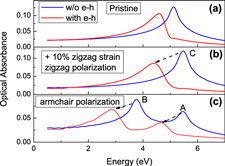
Many-electron effects on optical absorption spectra of strained graphene
-
- Journal:
- Journal of Materials Research / Volume 27 / Issue 2 / 28 January 2012
- Published online by Cambridge University Press:
- 20 December 2011, pp. 403-409
- Print publication:
- 28 January 2012
-
- Article
- Export citation
Synthesis of In2−xGexO3 nanopowders for thermoelectric applications
-
- Journal:
- Journal of Materials Research / Volume 27 / Issue 2 / 28 January 2012
- Published online by Cambridge University Press:
- 20 December 2011, pp. 500-505
- Print publication:
- 28 January 2012
-
- Article
- Export citation

An approach to the three-dimensional simulations of the Bosch process
-
- Journal:
- Journal of Materials Research / Volume 27 / Issue 5 / 14 March 2012
- Published online by Cambridge University Press:
- 20 December 2011, pp. 793-798
- Print publication:
- 14 March 2012
-
- Article
- Export citation
JMR volume 26 issue 24 Cover and Back matter
-
- Journal:
- Journal of Materials Research / Volume 26 / Issue 24 / 28 December 2011
- Published online by Cambridge University Press:
- 19 December 2011, pp. b1-b3
- Print publication:
- 28 December 2011
-
- Article
-
- You have access
- Export citation
JMR volume 26 issue 24 Cover and Front matter
-
- Journal:
- Journal of Materials Research / Volume 26 / Issue 24 / 28 December 2011
- Published online by Cambridge University Press:
- 19 December 2011, pp. f1-f5
- Print publication:
- 28 December 2011
-
- Article
-
- You have access
- Export citation

Band engineering of type-II ZnO/ZnSe heterostructures for solar cell applications
-
- Journal:
- Journal of Materials Research / Volume 27 / Issue 4 / 28 February 2012
- Published online by Cambridge University Press:
- 16 December 2011, pp. 730-733
- Print publication:
- 28 February 2012
-
- Article
- Export citation

Residual stress in as-deposited Al–Cu–Fe–B quasicrystalline thin films
-
- Journal:
- Journal of Materials Research / Volume 27 / Issue 5 / 14 March 2012
- Published online by Cambridge University Press:
- 16 December 2011, pp. 837-844
- Print publication:
- 14 March 2012
-
- Article
- Export citation
-
The residual stress in Al–Cu–Fe–B quasicrystalline thin films has been characterized by x-ray diffraction and the curvature method. Films with thicknesses in a range from 0.55 to 2.6 μm were deposited using magnetron sputtering on Si(100) substrates maintained at a temperature of 560 °C. It is found that the tensile stress in uncracked films as determined by the curvature method is close to that measured by a modified sin2ψ method using main diffraction peaks of the icosahedral structure and corresponds approximately to 1.1 GPa. This value is close to that of the thermal stress estimated from the mismatch between thermal expansion coefficients of the film and substrate, suggesting that thermal stress is the main source of residual stress. Increasing film thickness results in the development of cracks and partial delamination of the film, accompanied by the sudden decrease of the stress. The fracture toughness of the quasicrystalline films is estimated between 1.5 and 1.9 MPa
 .
.
 .
.
Finite element analysis of nanowire indentation on a flat substrate
-
- Journal:
- Journal of Materials Research / Volume 27 / Issue 3 / 14 February 2012
- Published online by Cambridge University Press:
- 16 December 2011, pp. 586-591
- Print publication:
- 14 February 2012
-
- Article
- Export citation

Fe64B22.8Nd6.6Y3.9Nb2.7 bulk nanocomposite magnets with improved size and magnetic properties
-
- Journal:
- Journal of Materials Research / Volume 27 / Issue 4 / 28 February 2012
- Published online by Cambridge University Press:
- 16 December 2011, pp. 725-729
- Print publication:
- 28 February 2012
-
- Article
- Export citation
