To save content items to your account,
please confirm that you agree to abide by our usage policies.
If this is the first time you use this feature, you will be asked to authorise Cambridge Core to connect with your account.
Find out more about saving content to .
To save content items to your Kindle, first ensure no-reply@cambridge.org
is added to your Approved Personal Document E-mail List under your Personal Document Settings
on the Manage Your Content and Devices page of your Amazon account. Then enter the ‘name’ part
of your Kindle email address below.
Find out more about saving to your Kindle.
Note you can select to save to either the @free.kindle.com or @kindle.com variations.
‘@free.kindle.com’ emails are free but can only be saved to your device when it is connected to wi-fi.
‘@kindle.com’ emails can be delivered even when you are not connected to wi-fi, but note that service fees apply.
Reliable and cost-effective techniques to process surface nanoscale metallic structures with controllable and complex nanomorphologies is important toward progress in technologies related to sensing, energy harvesting, information storage, and computing. Here we discuss how pulsed laser melting and the ensuing self-organization by dewetting of ultrathin films can be utilized to fabricate various nanomorphologies in a predictable manner. Ultrathin metal films (1–100 nm) on inert substrates like SiO2 are generally unstable, with their free energy resembling that of a spinodal system. The energy rate theory of self-organization, which is based on balancing the rate of thermodynamic free energy change to the rate of energy dissipation, predicts the appearance of characteristic length scales. This is borne out in experiments of nanosecond pulsed laser melting of a variety of metal films. We review this laser-based self-organization technique with various examples from the behavior of Ag and Co metals on SiO2 substrates. Specifically, film thickness and film roughness can be used to control dewetting length scales, whereas knowledge of the intermolecular forces responsible for the free energy of the system control the type of morphology. Furthermore, novel dewetting is observed that is attributable to nanoscale heating effects resulting from the thickness-dependent pulsed laser heating. These results help elucidate the basic mechanisms of pulsed laser induced dewetting of metal films, but they also provide potential routes for cost-effective nanomanufacturing of metallic surfaces for applications in sensing, energy harvesting, and information processing.
X-ray absorption fine structure spectroscopy (XAFS) is a powerful and versatile technique for studying structures of materials in chemistry, physics, biology and other fields. This textbook is a comprehensive, practical guide to carrying out and interpreting XAFS experiments. Assuming only undergraduate-level physics and mathematics, the textbook is ideally suited for graduate students in physics and chemistry starting XAFS-based research. It contains concise executable example programs in Mathematica 7. Supplementary material available at www.cambridge.org/9780521767750 includes Mathematica code from the book, related Mathematica programs, and worked data analysis examples. The textbook addresses experiment, theory, and data analysis, but is not tied to specific data analysis programs or philosophies. This makes it accessible to a broad audience in the sciences, and a useful guide for researchers entering the subject.
Alternating current (AC) electric fields generated by coplanar electrodes are used to externally direct the assembly of submicrometer sized disk-shaped zeolite particles. At the edge of the electrode, zeolite particles assemble in a brushlike structure that forms because of an interplay between an induced dipolar interaction and the drag force due to AC electroosmotic flow. Far from the electrode edge, where the fluid is quiescent, the disk-shaped particles form a nearly hexagonally close-packed structure, similar to suspensions of spherical particles. These results demonstrate a surprising generality of field-directed structures and offer promise for a hierarchical fabrication of nanostructures from zeolites.
The self-assembling properties of two rationally designed discotic π-conjugated hexaazatrinaphthylene (HATNA) molecules have been studied. In appropriate solvent systems, both ester-dodecyl-substituted and amide-dodecyl-substituted HATNAs self-assembled into nanowires and formed organogels. These nanowires could be easily transferred onto solid supports through spin casting for morphological study. In addition to the solution-based self-assembly method, solvent-vapor annealing (SVA) was explored as an alternative way to control the organization of supramolecular nanowires on surfaces. It was found that amorphous thin film of HATNA molecules transformed gradually into nanowire structures through a nucleation and growth mechanism during the SVA process. Several parameters including the preordering of molecules in the original thin film, choice of solvent vapors, annealing times, and surface properties were tuned to create different supramolecular organizations. Under particular conditions, aligned nanowires with preferential direction can be achieved.
In the literature, a few biological cells have been used as templates to form microcapsules of a variety of shapes and sizes. In this study, we proved the concept that living cells like platelets can be encapsulated with polyelectrolytes using electrostatic layer-by-layer self-assembly (LBL), and, most importantly, the encapsulation process did not induce activation of the platelets. Glycol-chitosan and poly-L-glutamic acid were electrostatically deposited onto platelets, and the encapsulation was confirmed using confocal laser scanning microscopy and scanning electron microscopy. Transmission electron microscopy observation further confirmed that the encapsulation process was mild and the activation of platelets was negligible. The encapsulation of living biological cells like platelets can serve as a model system in a wide range of biomedical applications including local and sustained drug delivery, immune protection of artificial tissues, and versatile artificial blood.
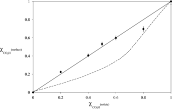
Self-assembled monolayers (SAMs) were formed on gold at anodic potentials from solutions containing two different alkyl thiosulfates, CH3(CH2)10S2O3Na and HO2C(CH2)10S2O3Na. The resulting two-component SAMs were analyzed using x-ray photoelectron spectroscopy to relate their compositions to those of the solutions from which they were adsorbed. This relationship was more linear than reported for analogous SAMs adsorbed from mixed solutions of alkanethiols. The wettability of these surfaces by water and by hexadecane was also measured and compared to analogous SAMs prepared by chemisorption of thiols from solution.
Molecular films have been extensively used for crystal growth. The Langmuir–Blodgett (LB) technique allows the oriented molecules film to be produced in a controllable manner. By controlling the LB film surface pressure and tuning quenching temperature of the supersaturated solution, single NaCl (100) crystal planes are successfully produced under the surface pressure of 30 mN/m with quenching temperature 5 °C of the NaCl supersaturated solution. The mechanism of single NaCl (100) crystal growth can be further explained based on the best matching between NaCl (100) crystal plane distance and the lattice parameter of LB film among all other crystal planes.
A novel nanoparticle self-assembly process is demonstrated. Nanoparticles were fabricated by a DC magnetron sputtering process. A silicon substrate was initially patterned with arrays of peak and valley photoresist structures using inexpensive patterning techniques. When the nanoparticles were deposited onto the prepatterned substrate, due to surface topography induced local increase in the electric field created by the charges on the nanoparticles, the nanoparticles were self-assembled onto the peaks of the structures and formed long nanowire arrays.
We demonstrate the formation of non-close-packed binary colloidal structures through a novel layer-by-layer directed self-assembly methodology. In this approach we deposit colloidal suspensions of particle concentration and controlled electrostatic potential onto a planar template with a periodic array of features that is able to trap the particles, nucleating ordered domains with a template-defined symmetry and periodicity that permits subsequent, sequential deposition to produce an ordered heterostructure. Specifically, a silicon template with a hole pattern formed by interference lithography that corresponds to [100] symmetry of a cubic system has been used. At low particle concentrations, and using a Debye length that is on the order of the particle diameter, ordered domains in which polystyrene (PS) particles occupy every other site in the template are formed. The remaining sites on the 2D template are then filled by identically sized silica particles using vertical deposition. This process is repeated to produce a second layer of the same structure. Upon removing the PS particles, a two-layer non-close-packed structure that is a half-unit-cell precursor to the diamond cubic structure is obtained. To our knowledge this is the first demonstration of colloidal self-assembly to obtain a non-close-packed multilayer structure. Challenges that remain in applying the approach to create extended three-dimensional structures are discussed.
We show that low-density nanoporous silica monoliths (aerogels), in contrast to the case of full-density silica, exhibit pronounced time-dependent deformation during indentation at room temperature. Logarithmic indentation creep and stress relaxation are revealed, with an exponential dependency of the creep constant on the applied stress. Such time-dependent deformation is attributed to stress corrosion fracture of nanoligaments that have a large surface-to-bulk atomic fraction.
One of the challenges in the development of molecular scale devices is the integration of nano-objects or molecules onto desired locations on a surface. This integration comprises their accurate positioning, their alignment, and the preservation of their functionality. Here, we proved how capillary assembly in combination with soft lithography can be used to perform DNA molecular combing to generate chips of isolated DNA strands for genetic analysis and diagnosis. The assembly of DNA molecules is achieved on a topologically micropatterned polydimethylsiloxane stamp inducing almost simultaneously the trapping and stretching of single molecules. The DNA molecules are then transferred onto aminopropyltriethoxysilane-coated surfaces. In fact, this technique offers the possibility to tightly control the experimental parameters to direct the assembly process. This technique does not induce a selection in size of the objects, therefore it can handle complex solutions of long (tens of kbp) but also shorter (a few thousands of bp) molecules directly in solution to allow the construction of future one-dimensional nanoscale building templates.
We investigated a simple and low-cost route for the formation of metallic nanodots on Si substrates ordered in size and position and laterally isolated by SiO2. The method was based on a two-step process: (i) the formation of a nanopattern of ordered cylindrical pores on oxidized Si substrates through self-assembly of diblock copolymers, and successive oxide dry etching down to the Si; (ii) the deposition of gold nanodots and thermal diffusion over the nanopatterned oxide substrates. After diffusion, the nanodot density outside the nanopores was found to decrease, and most of the nanodots were found to saturate the nanopores. The process was followed in situ by transmission electron microscopy (TEM) and ex situ by scanning electron microscopy (SEM) analysis for different thermal budgets. This patterned substrate can be used for catalyst mediated growth, for example, through vapor-liquid-solid (VLS), of nanowires for the formation of absorber materials in novel photovoltaic architectures.
Highly aligned microstrip patterns consisting of biaxial CaF2 nanorods have been successfully self-assembled by simply using capillary pressure. The alignment direction of the microstrips is perpendicular to the flux direction during nanorod growth. Aligning behavior and pattern width can be controlled by changing wetting time and surface tension of the liquid. Higher surface tension and longer wetting time result in wider pattern width and better alignment. Taller nanorod height also results in better pattern alignment. Simple and cost-effective self-aligned microstrip patterns can be potentially used as a template for various applications, such as superhydrophobic surfaces, tissue scaffolds, microchannels, and optical polarizers.
The heterocomponent films of polypyridine ruthenium(II) complexes and methyl viologen derivatives, and polypyridine ruthenium(II) complexes and alkyl chain derivatives have been successfully obtained using a layer-by-layer fabrication method. We determined their photocurrent generation properties and noted that the photocurrent generation strongly depended on the inner layer. A higher photocurrent generation in the donor–acceptor film was obtained than in a single-component film of the chromophore.
Thin-film aggregation characteristics of a series of oligothiophenes with a central thieno[3,4-b]thiophene ester unit and 4 (M5), 8 (M9), and 16 (M17) regioregular hexylthiophene units were investigated. These oligomers exhibited length-dependent self-assembly characteristics upon spin coating. M9 formed long fibers, while M5 and M17 formed random domains. Grazing incidence x-ray diffraction was performed to understand the reason for this length dependence. The M5 had a dominant ester–ester interaction that disrupted long-range order. The M9 morphology was due to a balance of orthogonal backbone and ester effects, which imposed long-range order on the M9 aggregates. Meanwhile, the M17 ester chain had a smaller relative contribution to packing and functioned as a molecular defect, disrupting long-range order. As a result, though the local self-assembly between monomers was very similar for the molecules, backbone length dependent changes in intermolecular forces dominated long-range structure. The analysis of self-assembly characteristics in these materials provides guidance in the design of organic conjugated materials for use in semiconductor devices.
An increasing number of technologies benefit from or require patterned surfaces on a micro- and nanoscale. Methods developed to structure polymer films can be adapted to fabricate low-cost patterned ceramics using nonlithographic techniques, for example, dewetting and phase separation in thin films. In this paper we describe a simple patterning process that does not require a template and is able to produce Fe2O3 microdots with a spatial periodicity. Our method involves the dewetting of a silicon substrate by a thin metal oxide precursor film, in which the liquid film breaks up because of fluctuations in the film thickness induced by solvent evaporation or an external applied electric field. The patterning is followed by a thermal treatment at 550 °C to produce crystalline Fe2O3 microdots with a diameter range of 200 nm to 3 μm.
The current study revealed the effects of reflow temperature and the reflow time on the interfacial embrittlement of SnBi/Cu joints. When the reflow temperature is below 220 °C, the joints reflowed for 150 min often fail in brittle mode because the Bi atoms from the SnBi solder easily segregated at the Cu3Sn/Cu interface. In contrast, Bi embrittlement did not occur for joints reflowed at above 260 °C for 150 min because the Bi particles were frozen in the Cu3Sn layer during the formation of intermetallic compounds (IMC) at the initial reflow stage, mainly located at the Cu3Sn grain boundary. It is interesting to note that the Bi embrittlement did occur when the joints were reflowed at above 260 °C for 250 min, which should be attributed to Bi diffusion. It is concluded that the Bi particles are frozen in the Cu3Sn layer with increasing reflow temperature, that cannot eliminate Bi embrittlement, and can only delay the occurrence of Bi embrittlement.
We have developed novel photovoltaic systems composed of the fullerene derivative (6,6)-phenyl C61 butyric acid methyl ester as electron acceptor with a second functional organic molecule, in this case bacteriochlorophyll c, as the light-harvesting and photosensitizing part. It was found that heat treatment of a thin film of bacteriochlorophyll c altered the morphological states of the aggregates and conductivity of the thin film could be regulated through the annealing process. Blended fullerene derivative and bacteriochlorophyll c thin films were fabricated on the surface of an indium-tin oxide/poly(ethylene dioxythiophene) doped with polystyrene sulfonic acid substrate layer and their photovoltaic properties were characterized and evaluated. Formation of fullerene-coordinated bacteriochlorophyll c complex was confirmed by changes in the visible absorption spectra and by FTIR. Such complexation promoted generation of photocurrent in the region of the Qyband and the current density of the thin film increased. A maximum incident photon-to-current conversion efficiency of 5.1% was attained at 745 nm.
Surface-enhanced Raman scattering (SERS) coupled with micro- or nanofluidics integrated into optofluidic devices offer many advantages over conventional SERS conducted under static conditions. Higher reproducibility, larger intensity, as well as greater enhancement can be achieved by efficient mixing of analytes and SERS enhancers under a continuous flow. Progress and advances in the past 10 years, including the design of channels and efficient mixing conditions, assemblies of SERS substrates for optimal enhancement, and advantages of optofluidic-SERS analysis, are reviewed. Recent results show that optofluidic-SERS effectively overcomes many of the difficulties and limitations plaguing conventional SERS and the novel technique has enormous application potential.
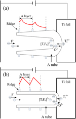
TiO2 nanotube arrays were synthesized by anodic oxidation on a pure titanium substrate in solutions containing 0.175 M NH4F composed of mixtures with different volumetric ratios of DI water and glycerol. According to the results of the current curve recorded during anodization, the time of the first sharp current slope (corresponding to the initial oxide layer formation time) was found to vary from 8 to 171 s depending not only upon the water content in the electrolytes but also upon the voltage. The current curves exhibit oscillation with different amplitudes and periods. In combination with the scanning electron microscope (SEM) images, a growth mechanism, layer-by-layer model, of TiO2 nanotube arrays was presented. Based on this mechanism, many phenomena that appeared during anodization can be reasonably explained. Our results would be helpful for the design of nanoarchitectures in related material systems.