To save content items to your account,
please confirm that you agree to abide by our usage policies.
If this is the first time you use this feature, you will be asked to authorise Cambridge Core to connect with your account.
Find out more about saving content to .
To save content items to your Kindle, first ensure no-reply@cambridge.org
is added to your Approved Personal Document E-mail List under your Personal Document Settings
on the Manage Your Content and Devices page of your Amazon account. Then enter the ‘name’ part
of your Kindle email address below.
Find out more about saving to your Kindle.
Note you can select to save to either the @free.kindle.com or @kindle.com variations.
‘@free.kindle.com’ emails are free but can only be saved to your device when it is connected to wi-fi.
‘@kindle.com’ emails can be delivered even when you are not connected to wi-fi, but note that service fees apply.
Operations called stamping, pressing and sometimes drawing involve clamping a sheet at it edges and forcing it into a die cavity with a punch as shown in Figure 17.1. The sheet is stretched rather than squeezed between the tools. Pressure on the draw beads controls how much additional material is drawn into the die cavity. In some cases there is a die, which reverses the movement of material after it is stretched over the punch.
DRAW BEADS
Draw beads (Figure 17.2) are used to create tension in the sheet being formed by preventing excessive drawing. As a sheet moves through a die bead it is bent three times and unbent three times. Each bend and each unbend there requires plastic work. Over each radius there is friction. Bending and unbending create resistance to movement of the sheet. If the resistance is sufficiently high, the sheet will be locked by the draw bead. The restraining force of the draw bead can be controlled by the height of the insert.
The restraining force has two components. One is caused by the work necessary to bend and unbend the sheet as it flows over the die bead and the other is the work to overcome friction. A crude estimate can be made of the restraining force per length resulting from the bending and unbending with the following simplifying assumptions:
work hardening, elastic core, movement of the neutral plane, and the difference between engineering strain and true strain (ε = e) are neglected.
The Swift cup test is the determination of the limiting drawing ratio for flat-bottom cups. In the Erichsen and Olsen tests, cups are formed by stretching over a hemispherical tool. The flanges are very large so little drawing occurs. The results depend on stretchability rather than drawability. The Olsen test is used in America and the Erichsen in Europe. Figure 20.1 shows the set up.
The Fukui conical cup test involves both stretching and drawing over a ball. The opening is much larger than the ball so a conical cup is developed. The flanges are allowed to draw in. Figure 20.2 shows the set up. A failed Fukui cup is shown in Figure 20.3.
Figure 20.4 shows comparison of the relative amounts of stretch and draw in these tests.
LDH TEST
The cupping tests discussed above are losing favor because of irreproducibility. Hecker attributed this to “insufficient size of the penetrator, inability to prevent inadvertent draw in of the flange and inconsistent lubrication.” He proposed the limiting dome height (LDH) test which uses the same tooling (4 inch diameter punch) as used to determine forming limit diagrams. The specimen width is adjusted to achieve plane-strain and the flange is clamped to prevent draw-in. The limiting dome height is greatest depth of cup formed with the flanges clamped. The LDH test results correlate better with the total elongation than with the uniform elongation as shown in Figures 20.5 and 20.6.
Direct-write, cryogenic electron beam-induced deposition (EBID) was performed by condensing methylcyclopentadienyl-platinum-trimethyl precursor onto a substrate at −155 °C, exposing the condensate by a 15 keV electron beam, and desorbing unexposed precursor molecules by heating the substrate to room temperature. Dependencies of film thickness, microstructure, and surface morphology on electron beam flux and fluence, and Monte Carlo simulations of electron interactions with the condensate are used to construct a model of cryogenic EBID that is contrasted to existing models of conventional, room temperature EBID. It is shown that material grown from a cryogenic condensate exhibits one of three distinct surface morphologies: a nanoporous mesh with a high surface-to-volume ratio; a smooth, continuous film analogous to material typically grown by room temperature EBID; or a film with a high degree of surface roughness, analogous to that of the cryogenic condensate. The surface morphology can be controlled reproducibly by the electron fluence used for exposure.
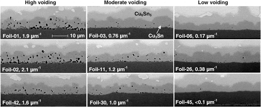
Soldering to Cu interconnect pads with Sn-containing alloys usually leads to the formation of a layered Cu3Sn/Cu6Sn5 structure on the pad/solder interface. Frequently, microscopic voids within Cu3Sn have been observed to develop during extended thermal aging. This phenomenon, commonly referred to as Kirkendall voiding, has been the subject of a number of studies and speculations but so far the root cause has remained unidentified. In the present work, 103 different Cu samples, consisting of 101 commercially electroplated Cu and two high-purity wrought Cu samples, were surveyed for voiding propensity. A high temperature anneal of the Cu samples before soldering was seen to significantly reduce the voiding level in subsequent thermal aging. For several void-prone Cu foils, the anneal led to significant pore formation inside the Cu. In the mean time, Cu grain growth in the void-prone foils showed impeded grain boundary mobility. Such behaviors suggested that the root cause for voiding is organic impurities incorporated in the Cu during electroplating, rather than the Kirkendall effect.
Phase diagrams are used in materials research and engineering to understand the interrelationship between composition, microstructure and process conditions. In complex systems, computational methods such as CALPHAD are employed to model thermodynamic properties for each phase and simulate multicomponent phase behavior. Written by recognized experts in the field, this is an introductory guide to the CALPHAD method, providing a theoretical and practical approach. Building on core thermodynamic principles, this 2007 book applies crystallography, first principles methods and experimental data to computational phase behavior modeling using the CALPHAD method. With a chapter dedicated to creating thermodynamic databases, the reader will be confident in assessing, optimizing and validating complex thermodynamic systems alongside database construction and manipulation. Several case studies put the methods into a practical context, making this suitable for use on advanced materials design and engineering courses and an invaluable reference to those using thermodynamic data in their research or simulations.
Ultrafast science—the study of highly complex and extremely short-lived transient events—has become an area of significant interest in the materials sciences, physics, chemistry, and biology. This article focuses on the state-of-the-art instrumentation and a few of the available probes and techniques, and intends to give a brief overview of the possibilities and challenges for ultrafast materials sciences and for the instrumentation that is required. The pulsed laser-material interactions are briefly introduced, since they are the principal methods to access and trigger ultrafast processes in materials. The associated time and length scales and a few experimental possibilities in the materials sciences are discussed in the first part of this article. The second part deals with the two most applicable types of pulsed probes, x-rays and electrons, and the associated methods to interrogate ultrafast processes. Emphasis is on their differences, capabilities, and limitations.
The impact of contact materials on the performance of nanostructured devices is expected to be significant. This is especially true since size scaling can increase the contact resistance and induce many unseen phenomenon and reactions that greatly impact device performance. Nanowire and nanoelectromechanical switches are two emerging nanoelectronic devices. Nanowires provide a unique opportunity to control the property of a material at an ultra-scaled dimension, whereas a nanoelectromechanical switch presents zero power consumption in its off state, as it is physically detached from the sensor anode. In this article, we specifically discuss contact material issues related to nanowire devices and nanoelectromechanical switches.
In this article, we review current research activities in contact material development for electronic and nanoelectronic devices. A fundamental issue in contact materials research is to understand and control interfacial reactions and phenomena that modify the expected device performance. These reactions have become more challenging and more difficult to control as new materials have been introduced and as device sizes have entered the deep nanoscale. To provide an overview of this field of inquiry, this issue of MRS Bulletin includes articles on gate and contact materials for Si-based devices, junction contact materials for Si-based devices, and contact materials for alternate channel substrates (Ge and III–V), nanodevices.