Refine search
Actions for selected content:
1808 results in Circuits and systems
Reviews
-
- Book:
- Fast Techniques for Integrated Circuit Design
- Published online:
- 08 August 2019
- Print publication:
- 15 August 2019, pp ii-ii
-
- Chapter
- Export citation
Contents
-
- Book:
- Fast Techniques for Integrated Circuit Design
- Published online:
- 08 August 2019
- Print publication:
- 15 August 2019, pp vii-viii
-
- Chapter
- Export citation
Copyright page
-
- Book:
- Fast Techniques for Integrated Circuit Design
- Published online:
- 08 August 2019
- Print publication:
- 15 August 2019, pp iv-iv
-
- Chapter
- Export citation
4 - Electromagnetism: Fundamentals
-
- Book:
- Fast Techniques for Integrated Circuit Design
- Published online:
- 08 August 2019
- Print publication:
- 15 August 2019, pp 50-100
-
- Chapter
- Export citation
Appendices
-
- Book:
- Fast Techniques for Integrated Circuit Design
- Published online:
- 08 August 2019
- Print publication:
- 15 August 2019, pp 234-241
-
- Chapter
- Export citation
3 - Higher Level Amplifier Stages
-
- Book:
- Fast Techniques for Integrated Circuit Design
- Published online:
- 08 August 2019
- Print publication:
- 15 August 2019, pp 31-49
-
- Chapter
- Export citation
Dedication
-
- Book:
- Fast Techniques for Integrated Circuit Design
- Published online:
- 08 August 2019
- Print publication:
- 15 August 2019, pp v-vi
-
- Chapter
- Export citation
Appendix B - Useful Mathematical Relationships
-
- Book:
- Fast Techniques for Integrated Circuit Design
- Published online:
- 08 August 2019
- Print publication:
- 15 August 2019, pp 239-241
-
- Chapter
- Export citation
1 - General Guidelines in Estimation Analysis in Integrated Circuits
-
- Book:
- Fast Techniques for Integrated Circuit Design
- Published online:
- 08 August 2019
- Print publication:
- 15 August 2019, pp 1-3
-
- Chapter
-
- You have access
- HTML
- Export citation
Appendix A - Basic Transistor and Technology Model
-
- Book:
- Fast Techniques for Integrated Circuit Design
- Published online:
- 08 August 2019
- Print publication:
- 15 August 2019, pp 234-238
-
- Chapter
- Export citation
2 - Basic Amplifier Stages
-
- Book:
- Fast Techniques for Integrated Circuit Design
- Published online:
- 08 August 2019
- Print publication:
- 15 August 2019, pp 4-30
-
- Chapter
- Export citation
6 - Electromagnetic Field Simulators
-
- Book:
- Fast Techniques for Integrated Circuit Design
- Published online:
- 08 August 2019
- Print publication:
- 15 August 2019, pp 151-164
-
- Chapter
- Export citation
Index
-
- Book:
- Fast Techniques for Integrated Circuit Design
- Published online:
- 08 August 2019
- Print publication:
- 15 August 2019, pp 242-246
-
- Chapter
- Export citation
7 - System Aspects
-
- Book:
- Fast Techniques for Integrated Circuit Design
- Published online:
- 08 August 2019
- Print publication:
- 15 August 2019, pp 165-233
-
- Chapter
- Export citation

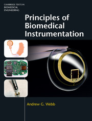
Principles of Biomedical Instrumentation
-
- Published online:
- 11 August 2019
- Print publication:
- 11 January 2018
-
- Textbook
- Export citation

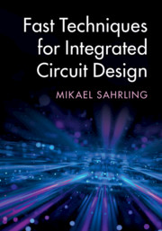
Fast Techniques for Integrated Circuit Design
-
- Published online:
- 08 August 2019
- Print publication:
- 15 August 2019

Electrical Machines
-
- Published online:
- 03 August 2019
- Print publication:
- 04 October 2017
-
- Textbook
- Export citation
2 - 5G Transceivers from Requirements to System Models and Analysis
-
- Book:
- Millimeter-Wave Circuits for 5G and Radar
- Published online:
- 31 May 2019
- Print publication:
- 20 June 2019, pp 18-54
-
- Chapter
- Export citation
14 - FinFET Process Technology for RF and Millimeter-Wave Applications
-
- Book:
- Millimeter-Wave Circuits for 5G and Radar
- Published online:
- 31 May 2019
- Print publication:
- 20 June 2019, pp 400-431
-
- Chapter
- Export citation
Foreword
-
- Book:
- Millimeter-Wave Circuits for 5G and Radar
- Published online:
- 31 May 2019
- Print publication:
- 20 June 2019, pp xvii-xviii
-
- Chapter
- Export citation
