Refine search
Actions for selected content:
106100 results in Materials Science

Total ionizing dose-hardened carbon nanotube thin-film transistors with silicon oxynitride gate dielectrics
-
- Journal:
- MRS Communications / Volume 1 / Issue 1 / November 2011
- Published online by Cambridge University Press:
- 25 August 2011, pp. 27-31
- Print publication:
- November 2011
-
- Article
- Export citation

A study on surfactant-free growth of silver-carbon nanocables by H2SO4-mediated hydrothermal process
-
- Journal:
- Journal of Materials Research / Volume 26 / Issue 21 / 14 November 2011
- Published online by Cambridge University Press:
- 25 August 2011, pp. 2780-2794
- Print publication:
- 14 November 2011
-
- Article
- Export citation

Compositional and microstructural evolution during annealing of Terfenol-D nanoparticulate films
-
- Journal:
- Journal of Materials Research / Volume 26 / Issue 20 / 28 October 2011
- Published online by Cambridge University Press:
- 24 August 2011, pp. 2672-2681
- Print publication:
- 28 October 2011
-
- Article
- Export citation

Strained structure of differently prepared amorphous TiO2 nanoparticle: Molecular dynamics study
-
- Journal:
- Journal of Materials Research / Volume 26 / Issue 20 / 28 October 2011
- Published online by Cambridge University Press:
- 24 August 2011, pp. 2604-2611
- Print publication:
- 28 October 2011
-
- Article
- Export citation

Germanium nanowire synthesis using a localized heat source and a comparison to synthesis in a uniform temperature environment
-
- Journal:
- Journal of Materials Research / Volume 26 / Issue 17 / 14 September 2011
- Published online by Cambridge University Press:
- 24 August 2011, pp. 2215-2223
- Print publication:
- 14 September 2011
-
- Article
- Export citation

A comparative study of anodized titania nanotube architectures in aqueous and nonaqueous solutions
-
- Journal:
- Journal of Materials Research / Volume 26 / Issue 20 / 28 October 2011
- Published online by Cambridge University Press:
- 24 August 2011, pp. 2612-2623
- Print publication:
- 28 October 2011
-
- Article
- Export citation

Fabrication of carbon-nanotube-based sensor array and interference study
-
- Journal:
- Journal of Materials Research / Volume 26 / Issue 16 / 28 August 2011
- Published online by Cambridge University Press:
- 23 August 2011, pp. 2017-2023
- Print publication:
- 28 August 2011
-
- Article
- Export citation
JMR volume 26 issue 16 Cover and Back matter
-
- Journal:
- Journal of Materials Research / Volume 26 / Issue 16 / 28 August 2011
- Published online by Cambridge University Press:
- 23 August 2011, pp. b1-b3
- Print publication:
- 28 August 2011
-
- Article
-
- You have access
- Export citation
JMR volume 26 issue 16 Cover and Front matter
-
- Journal:
- Journal of Materials Research / Volume 26 / Issue 16 / 28 August 2011
- Published online by Cambridge University Press:
- 23 August 2011, pp. f1-f4
- Print publication:
- 28 August 2011
-
- Article
-
- You have access
- Export citation

Scanning nonlinear dielectric microscopy
-
- Journal:
- Journal of Materials Research / Volume 26 / Issue 16 / 28 August 2011
- Published online by Cambridge University Press:
- 23 August 2011, pp. 2007-2016
- Print publication:
- 28 August 2011
-
- Article
- Export citation

Growth of carbon nanocoils using Fe–Sn–O catalyst film prepared by a spin-coating method
-
- Journal:
- Journal of Materials Research / Volume 26 / Issue 16 / 28 August 2011
- Published online by Cambridge University Press:
- 23 August 2011, pp. 2024-2032
- Print publication:
- 28 August 2011
-
- Article
- Export citation

Doping of semiconductor nanowires
-
- Journal:
- Journal of Materials Research / Volume 26 / Issue 17 / 14 September 2011
- Published online by Cambridge University Press:
- 22 August 2011, pp. 2142-2156
- Print publication:
- 14 September 2011
-
- Article
- Export citation

Zn–Ni–Co–O wide-band-gap p-type conductive oxides with high work functions
-
- Journal:
- MRS Communications / Volume 1 / Issue 1 / November 2011
- Published online by Cambridge University Press:
- 19 August 2011, pp. 23-26
- Print publication:
- November 2011
-
- Article
- Export citation

Localized recrystallization and cracking of lead-free solder interconnections under thermal cycling
-
- Journal:
- Journal of Materials Research / Volume 26 / Issue 16 / 28 August 2011
- Published online by Cambridge University Press:
- 16 August 2011, pp. 2103-2116
- Print publication:
- 28 August 2011
-
- Article
- Export citation
Large-scale integration of single-walled carbon nanotubes and graphene into sensors and devices using dielectrophoresis: A review – ERRATUM
-
- Journal:
- Journal of Materials Research / Volume 26 / Issue 16 / 28 August 2011
- Published online by Cambridge University Press:
- 15 August 2011, p. 2123
- Print publication:
- 28 August 2011
-
- Article
-
- You have access
- HTML
- Export citation

Surface-induced effects in GaN nanowires
-
- Journal:
- Journal of Materials Research / Volume 26 / Issue 17 / 14 September 2011
- Published online by Cambridge University Press:
- 15 August 2011, pp. 2157-2168
- Print publication:
- 14 September 2011
-
- Article
- Export citation

Indentation creep revisited
-
- Journal:
- Journal of Materials Research / Volume 27 / Issue 1 / 14 January 2012
- Published online by Cambridge University Press:
- 15 August 2011, pp. 3-11
- Print publication:
- 14 January 2012
-
- Article
- Export citation

Insights on uniaxial compression of WS2 inorganic fullerenes: A finite element study
-
- Journal:
- Journal of Materials Research / Volume 27 / Issue 1 / 14 January 2012
- Published online by Cambridge University Press:
- 15 August 2011, pp. 161-166
- Print publication:
- 14 January 2012
-
- Article
- Export citation
Effects of high-temperature ambient on cyclic fatigue of La0.8Sr0.2MnO3+δ
-
- Journal:
- Journal of Materials Research / Volume 26 / Issue 18 / 28 September 2011
- Published online by Cambridge University Press:
- 15 August 2011, pp. 2450-2457
- Print publication:
- 28 September 2011
-
- Article
- Export citation
-
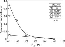
The effects of water vapor and oxygen on the cyclic fatigue behavior of oxygen-excess La0.8Sr0.2MnO3+δ (LSM) were investigated under three-point bending at 1273 K. Because the fatigue life did not obviously depend on the number of cycles, which also represented the effective time of the applied stress, the fracture was presumed to not be significantly controlled by stress-corrosion cracking. Under a low oxygen partial pressure (
 ), however, wet exposure inhibited both fatigue fracture and permanent deformation, in which the LSM crystal lattice was distorted and the unit cell free volume was reduced. Under a high
  , on the contrary, the crystal symmetry was increased by the wet exposure. The inhibition of fatigue fracture and deformation at both high
  and low
  was probably caused by retardation of lanthanum diffusion through its vacancies.
Self-organization of SrRuO3 nanowires on ordered oxide surface terminations
-
- Journal:
- MRS Communications / Volume 1 / Issue 1 / November 2011
- Published online by Cambridge University Press:
- 12 August 2011, pp. 17-21
- Print publication:
- November 2011
-
- Article
- Export citation
