To save content items to your account,
please confirm that you agree to abide by our usage policies.
If this is the first time you use this feature, you will be asked to authorise Cambridge Core to connect with your account.
Find out more about saving content to .
To save content items to your Kindle, first ensure no-reply@cambridge.org
is added to your Approved Personal Document E-mail List under your Personal Document Settings
on the Manage Your Content and Devices page of your Amazon account. Then enter the ‘name’ part
of your Kindle email address below.
Find out more about saving to your Kindle.
Note you can select to save to either the @free.kindle.com or @kindle.com variations.
‘@free.kindle.com’ emails are free but can only be saved to your device when it is connected to wi-fi.
‘@kindle.com’ emails can be delivered even when you are not connected to wi-fi, but note that service fees apply.
We report on the fabrication and tunneling characteristics of pulsed-laser deposited LaSrMnO (LSMO)/PbZrTiO(PZT)/LSMO/SrTiO3 magnetic tunnel junctions. The trilayer films show magnetic onset at about 360 K with ferromagnetic hysteresis and uniaxial magnetic behavior at room temperature. The microscopic studies show that the effective barrier thickness is reduced due to the presence of defects in the barrier region. Tunneling magnetoresistance measurements were performed on several samples. Our results suggest that the asymmetric deformation of the barrier potential profile induced by the ferroelectric polarization of PZT influences the tunneling characteristics and can be used for electrically controlled readout in quantum computing schemes.
YVO4: 10%RE3+ (RE = Eu, Sm, Dy, Er) nanophosphors have been synthesized by a facile modified hydrothermal technology to obtain the high purity. The key procedure for this hydrothermal process is the adding order of precursors, in which excess sodium vanadate should be added in the solution of rare earth nitrates. The microstructure (crystal phase, morphology, particle size) of these phosphors are characterized by x-ray powder diffraction, scanning electron microscope, and transmission electron microscope, which indicates that there are some cube-like crystals with tetragonal zircon structure and the average particle size is approximately 40 nm. The luminescent behaviors for the four rare earth ion-activated YVO4 nanophosphors have been studied, and, for YVO4: 10%Eu3+ nanophosphors in particular, it is found that a different hydrothermal process influences the phase composition, microstructure, and photoluminescence. This result suggests that the hydrothermal synthesis process (by adding sodium vanadate to the solution of rare earth nitrates) is favorable for YVO4 nanophosphor to obtain pure phase, small particle size, long luminescent lifetime, and high luminescence quantum efficiency.
The work-hardening mechanisms of the Ti60Cu14Ni12Sn4Nb10 nanocomposite alloy were studied. This material is composed of micrometer-sized dendrites embedded in a nanostructured eutectic matrix and a CuTi2 intermetallic phase. Our study shows that, in the as-quenched state, the nanostructured eutectic matrix behaves softer than the dendrites. During mechanical deformation, both the dendrites and the eutectic matrix harden, whereas the hardness of the CuTi2 intermetallic phase remains unaltered. The high strength of the dendrites is caused by the interplay between solid solution hardening and dislocation networks during plastic flow. Interestingly, the mechanical hardening of the nanoeutectic matrix is also assisted by a martensitic transformation of the NiTi phase. Transmission electron microscopy studies clearly show that the martensitic transformation of this phase is accompanied with grain size refinement, which also plays a role in the deformation-induced mechanical hardening.
A uniaxial synchro-compression test of a cylindrical bulk metallic glass (BMG) specimen along with a crystalline metallic ring having an inner diameter much larger than the specimen’s diameter and thereby without radial confinement on the BMG specimen was performed. The plastic deformation behavior of a conventional Zr65Cu17.5Ni10Al7.5 BMG under synchro-compression with a cupper ring was investigated. It was found that remarkably plastic deformation in the inherently brittle BMG could occur under the uniaxial stress state as the loading area of the cupper ring was sufficiently large, and multiplication of the shear band on the synergistically deformed BMG specimen could be accomplished. The synergistic effect of the crystalline metal on the plastic deformation behavior of the BMG was attributed to the reduced thermal softening extent inside the shear bands that resulted from the restraining effect of the copper ring on the spring-back action of the testing machine.
Bismuth-doped (Ba1−xCax)TiO3 ceramics (x = 0.10, Bi-BCT) were prepared by a conventional solid-state reaction technique. An abnormal double-like hysteresis polarization–electric (P–E) loop was observed at room temperature for aged Bi-BCT. Raman scattering gives critical evidence for the formation of O2− vacancies in Bi-BCT. The change from the single P–E loops in the fresh samples to the double loops in the aged samples excludes the existence of a ferroelectric–antiferroelectric transition in Bi-BCT. A reversible domain switching mechanism resulting from a symmetry-conforming short-range ordering of point defects gives a reasonable explanation for the naturally age-induced double-like P–E loops in Bi-BCT.
Microstructure features of five electrodeposited coppers with different grain sizes were systematically characterized by using transmission electron microscopy (TEM) observations and x-ray diffraction (XRD) analysis. Based on the experimental observations, two mechanisms for the grain refinement in electrodeposited copper were identified: (i) twin–twin intersection can directly create grains with large-angle boundaries as small as 10 nm and (ii) grains can also be refined via formation of dislocation cells, transformation of dislocation cell walls into sub-boundaries with small misorientations, and evolution of sub-boundaries into highly misoriented grain boundaries. Besides, dislocations are also effective to cut twin lamellas into pieces and make twin boundaries curved and round.
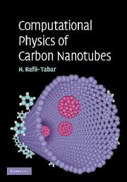
Carbon nanotubes are the fabric of nanotechnology. Investigation into their properties has become one of the most active fields of modern research. This book presents the key computational modelling and numerical simulation tools to investigate carbon nanotube characteristics. In particular, methods applied to geometry and bonding, mechanical, thermal, transport and storage properties are addressed. The first half describes classic statistical and quantum mechanical simulation techniques, (including molecular dynamics, Monte Carlo simulations and ab initio molecular dynamics), atomistic theory and continuum based methods. The second half discusses the application of these numerical simulation tools to emerging fields such as nanofluidics and nanomechanics. With selected experimental results to help clarify theoretical concepts, this is a self-contained book that will be of interest to researchers in a broad range of disciplines, including nanotechnology, engineering, materials science and physics.
This book is devoted to the main aspects of the physics of recombination in semiconductors. It is the first book to deal exclusively and comprehensively with the subject, and as such is a self-contained volume, introducing the concepts and mechanisms of recombination from a fundamental point of view. Professor Landsberg is an internationally acknowledged expert in this field, and while not neglecting the occasional historical insights, he takes the reader to the frontiers of current research. Following initial chapters on semiconductor statistics and recombination statistics, the text moves on to examine the main recombination mechanisms: Auger effects, impact ionisation, radiative recombination, defect and multiphonon recombination. The final chapter deals with the topical subject of quantum wells and low-dimensional structures. Altogether the book covers a remarkably wide area of semiconductor physics. The book will be of importance to physicists, electronic engineers and applied mathematicians who are studying or researching the physics and applications of semiconductors. Some parts of the book will be accessible to final-year undergraduates.
This book describes the application of high-temperature superconducting materials to microwave devices and systems. It deals with the fundamentals of the interaction between microwaves and superconductors, and includes a basic description of how microwave devices can be constructed using these materials. Since the discovery of high-temperature superconductors in 1986 there has been an enormous effort worldwide to develop and characterize these materials. Work on applications has proceeded more slowly however. Nevertheless, commercial applications are now beginning to be possible, including use in passive microwave devices. The advantages of using high-temperature superconductors in these devices is carefully described by the author, enabling scientists and engineers to form a complete understanding of the subject. The rest of the book is devoted to examples of superconducting microwave filters, antennas and systems. The examples chosen relate not only to what can be achieved at present, but indicate the trends for future research and what may be expected for superconducting devices in the future.
This book describes for the first time in a modern text the fundamental principles on which solid state chemistry is based. In this sense it differs from other books on the subject, which tend to concentrate only on a description of materials.Topics include solid (ceramic) electrolytes, glasses, polymer electrolytes, intercalation electrodes, interfaces and applications. The different nature of ionic conductivity in ceramic, glassy and polymer electrolytes is described, as are the thermodynamics and kinetics of intercalation reactions. The interface between solid electrolytes and electrodes is discussed and contrasted with more conventional liquid state electrochemistry.The text provides an essential foundation for postgraduates and others entering the field for the first time and will also be of value in advanced undergraduate courses.
Crystallization is an important purification process used in a broad range of industries, including pharmaceuticals, foods, and bulk chemicals. In recent years, molecular modeling has emerged as a useful tool in the analysis and solution of problems associated with crystallization. Modeling allows more focused experimentation based on structural and energetic calculations instead of intuition and trial and error. This book is the first to offer a general introduction to molecular modeling techniques and their application in crystallization. After explaining the basic concepts of molecular modeling and crystallization, the book goes on to discuss how modeling techniques are used to solve a variety of practical problems related to crystal size, shape, internal structure, and properties. With chapters written by leading experts and an emphasis on problem-solving, this book will appeal to scientists, engineers, and graduate students involved in research and the production of crystalline materials.
The elucidation of the effects of structurally extended defects on electronic properties of materials is especially important in view of the current advances in electronic device development that involve defect control and engineering at the nanometer level. This book surveys the properties, effects, roles and characterization of extended defects in semiconductors. The basic properties of extended defects (dislocations, stacking faults, grain boundaries, and precipitates) are outlined, and their effect on the electronic properties of semiconductors, their role in semiconductor devices, and techniques for their characterization are discussed. These topics are among the central issues in the investigation and applications of semiconductors and in the operation of semiconductor devices. The authors preface their treatment with an introduction to semiconductor materials and conclude with a chapter on point defect maldistributions. This text is suitable for advanced undergraduate and graduate students in materials science and engineering, and for those studying semiconductor physics.
Recent developments in chemical synthesis, nanoscale assembly, and molecular-scale measurements enable the extension of the concept of macroscopic machines to the molecular and supramolecular levels. Molecular machines are capable of performing mechanical movements in response to external stimuli. They offer the potential to couple electrical or other forms of energy to mechanical action at the nano- and molecular scales. Working hierarchically and in concert, they can form actuators referred to as artificial muscles, in analogy to biological systems. We describe the principles behind driven motion and assembly at the molecular scale and recent advances in the field of molecular-level electromechanical machines, molecular motors, and artificial muscles. We discuss the challenges and successes in making these assemblies work cooperatively to function at larger scales.
We report that various metallic glassy nanostructures including nanoridges, nanocones, nanowires, nanospheres, and nanoscale-striped patterns are spontaneously formed on the fracture surface of bulk metallic glasses at room temperature. A clear correlation between the dimensions of these nanostructures and the size of the plastic zone at the crack tip has been found, providing a way to control nanostructure sizes by controlling the plastic zone size intrinsically or extrinsically. This approach to forming metallic glassy nanostructures also has implications for understanding the deformation and fracture mechanisms of metallic glasses.
Antiferroelectric (AFE) Pb0.92La0.08Zr0.95Ti0.05O3 (PLZT) films were grown on nickel foils with lanthanum nickel oxide buffer by chemical solution deposition. We observed field-induced AFE-to-ferroelectric (FE) phase transition. The electric field for the AFE-to-FE phase transition (EAF ≈ 270 kV/cm) and that for the reverse phase transition (EFA ≈ 230 kV/cm) were measured at room temperature on samples with PLZT films of ≈1-µm thickness. Relative permittivity of ≈560 and dielectric loss of <0.05 were measured near zero DC bias field. Hysteresis loop analysis showed that energy densities of ≈53 and 37 J/cm3 can be stored and recovered from the film-on-foil capacitors at 25 and 150 °C, respectively. Highly accelerated life tests were conducted. The projected mean time to failure is >5000 h when the capacitors are operated at room temperature with an applied field of ≈300 kV/cm.