Refine search
Actions for selected content:
106117 results in Materials Science
Index
-
- Book:
- Ultrasonic Guided Waves in Solid Media
- Published online:
- 05 July 2014
- Print publication:
- 11 August 2014, pp 507-512
-
- Chapter
- Export citation
Appendix B - Basic Formulas and Concepts in the Theory of Elasticity
-
- Book:
- Ultrasonic Guided Waves in Solid Media
- Published online:
- 05 July 2014
- Print publication:
- 11 August 2014, pp 445-455
-
- Chapter
- Export citation
16 - Guided Wave Phased Arrays in Piping
-
- Book:
- Ultrasonic Guided Waves in Solid Media
- Published online:
- 05 July 2014
- Print publication:
- 11 August 2014, pp 294-322
-
- Chapter
- Export citation

A look into Cu-based shape memory alloys: Present scenario and future prospects
-
- Journal:
- Journal of Materials Research / Volume 29 / Issue 16 / 28 August 2014
- Published online by Cambridge University Press:
- 07 August 2014, pp. 1681-1698
- Print publication:
- 28 August 2014
-
- Article
- Export citation

Controlled loading of paramagnetic gadolinium oxide nanoplates in PMAO-g-PEG as effective T1-weighted MRI contrast agents
-
- Journal:
- Journal of Materials Research / Volume 29 / Issue 15 / 14 August 2014
- Published online by Cambridge University Press:
- 07 August 2014, pp. 1626-1634
- Print publication:
- 14 August 2014
-
- Article
- Export citation

Strategies for the selective volume sintering of ceramics
-
- Journal:
- Journal of Materials Research / Volume 29 / Issue 17 / 14 September 2014
- Published online by Cambridge University Press:
- 07 August 2014, pp. 2095-2099
- Print publication:
- 14 September 2014
-
- Article
- Export citation
A technique for determining coefficients of the “stress–strain” diagram by nanoscratch test results
-
- Journal:
- Journal of Materials Research / Volume 29 / Issue 16 / 28 August 2014
- Published online by Cambridge University Press:
- 07 August 2014, pp. 1730-1736
- Print publication:
- 28 August 2014
-
- Article
- Export citation
Biological Materials Science
- Biological Materials, Bioinspired Materials, and Biomaterials
-
- Published online:
- 05 August 2014
- Print publication:
- 31 July 2014
Thermodynamics of Surfaces and Interfaces
- Concepts in Inorganic Materials
-
- Published online:
- 05 August 2014
- Print publication:
- 17 July 2014
Cellular Solids
- Structure and Properties
-
- Published online:
- 05 August 2014
- Print publication:
- 01 May 1997
X-ray powder diffraction data for monosodium salt azobarbituric acid dihydrate [C8H5N6O6Na.2H2O]
-
- Journal:
- Powder Diffraction / Volume 29 / Issue 4 / December 2014
- Published online by Cambridge University Press:
- 04 August 2014, pp. 383-384
-
- Article
- Export citation
Additive nanomanufacturing – A review
-
- Journal:
- Journal of Materials Research / Volume 29 / Issue 17 / 14 September 2014
- Published online by Cambridge University Press:
- 04 August 2014, pp. 1792-1816
- Print publication:
- 14 September 2014
-
- Article
- Export citation
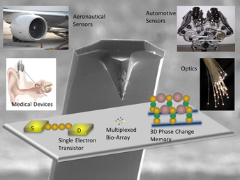
Phase change materials and phase change memory
-
- Journal:
- MRS Bulletin / Volume 39 / Issue 8 / August 2014
- Published online by Cambridge University Press:
- 14 August 2014, pp. 703-710
- Print publication:
- August 2014
-
- Article
- Export citation
Scaling computation with silicon photonics
-
- Journal:
- MRS Bulletin / Volume 39 / Issue 8 / August 2014
- Published online by Cambridge University Press:
- 14 August 2014, pp. 687-695
- Print publication:
- August 2014
-
- Article
- Export citation
Meet Our Authors
-
- Journal:
- MRS Bulletin / Volume 39 / Issue 8 / August 2014
- Published online by Cambridge University Press:
- 14 August 2014, pp. 663-667
- Print publication:
- August 2014
-
- Article
-
- You have access
- HTML
- Export citation
Energy Focus: Rock-salt LiBH4 phase solid electrolyte shows enhanced Li+ conduction
-
- Journal:
- MRS Bulletin / Volume 39 / Issue 8 / August 2014
- Published online by Cambridge University Press:
- 14 August 2014, p. 653
- Print publication:
- August 2014
-
- Article
-
- You have access
- HTML
- Export citation
Electronic Structure of Materials Rajendra Prasad: Taylor & Francis/CRC Press, 2013, 447 pages, $89.95, ISBN 978-1-4665-0468-4
-
- Journal:
- MRS Bulletin / Volume 39 / Issue 8 / August 2014
- Published online by Cambridge University Press:
- 14 August 2014, p. 748
- Print publication:
- August 2014
-
- Article
-
- You have access
- HTML
- Export citation
Two-dimensional materials for electronic applications
-
- Journal:
- MRS Bulletin / Volume 39 / Issue 8 / August 2014
- Published online by Cambridge University Press:
- 14 August 2014, pp. 711-718
- Print publication:
- August 2014
-
- Article
- Export citation

Emerging materials for microelectromechanical systems at elevated temperatures
-
- Journal:
- Journal of Materials Research / Volume 29 / Issue 15 / 14 August 2014
- Published online by Cambridge University Press:
- 01 August 2014, pp. 1597-1608
- Print publication:
- 14 August 2014
-
- Article
- Export citation
Breaking the 10-nm grain size barrier in ultrahard metals
-
- Journal:
- MRS Bulletin / Volume 39 / Issue 8 / August 2014
- Published online by Cambridge University Press:
- 14 August 2014, p. 653
- Print publication:
- August 2014
-
- Article
-
- You have access
- HTML
- Export citation
