Refine search
Actions for selected content:
106117 results in Materials Science

Further investigation of particle reinforced aluminum matrix composites by indentation experiments
-
- Journal:
- Journal of Materials Research / Volume 29 / Issue 4 / 28 February 2014
- Published online by Cambridge University Press:
- 14 February 2014, pp. 586-595
- Print publication:
- 28 February 2014
-
- Article
- Export citation

Spin-coated P3HT:Aminated carbon microsphere composite films for polymer solar cells
-
- Journal:
- Journal of Materials Research / Volume 29 / Issue 4 / 28 February 2014
- Published online by Cambridge University Press:
- 13 February 2014, pp. 492-500
- Print publication:
- 28 February 2014
-
- Article
- Export citation

Microstructure evolution of gas-atomized Fe–6.5 wt% Si droplets
-
- Journal:
- Journal of Materials Research / Volume 29 / Issue 4 / 28 February 2014
- Published online by Cambridge University Press:
- 13 February 2014, pp. 527-534
- Print publication:
- 28 February 2014
-
- Article
- Export citation
-
The magnetic Fe–6.5 wt% Si powder was produced by gas atomization and its microstructure was also investigated. The secondary dendritic arm spacing (SDAS) is related to the droplet size,
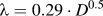 ${\rm{\lambda }} = 0.29 \cdot {D^{0.5}}$ , and the numerical solidification model was applied to the system, giving rise to the correlation of microstructure to the solidification process of the droplet. It is found that the solid fraction at the end of recalescence is strongly dependent on the undercooling achieved before nucleation; the chances for the smaller droplets to form the grain-refined microstructures are less than the larger ones. Furthermore, the SDAS is strongly influenced by the cooling rate of post-recalescence solidification, and the relationship can be expressed as follows,
 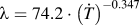 ${\rm{\lambda }} = 74.2 \cdot {\left( {\dot T} \right)^{ - 0.347}}$ . Then, the growth of the SDAS is driven by the solute diffusion of the interdendritic liquids, leading to a coarsening phenomenon, shown in a cubic root law of local solidification time,
 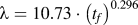 ${\rm{\lambda }} = 10.73 \cdot {\left( {{t_f}} \right)^{0.296}}$ .


Understanding the brittleness of metallic glasses through dynamic clusters
-
- Journal:
- Journal of Materials Research / Volume 29 / Issue 4 / 28 February 2014
- Published online by Cambridge University Press:
- 13 February 2014, pp. 561-568
- Print publication:
- 28 February 2014
-
- Article
- Export citation

Influence of film thickness and surface orientation on melting behaviors of copper nanofilms
-
- Journal:
- Journal of Materials Research / Volume 29 / Issue 4 / 28 February 2014
- Published online by Cambridge University Press:
- 13 February 2014, pp. 535-541
- Print publication:
- 28 February 2014
-
- Article
- Export citation
Electron-driven engineering of graphene – RETRACTION
-
- Journal:
- Journal of Materials Research / Volume 29 / Issue 4 / 28 February 2014
- Published online by Cambridge University Press:
- 13 February 2014, p. 604
- Print publication:
- 28 February 2014
-
- Article
-
- You have access
- HTML
- Export citation
Adhesion, micro- strain and corrosion behavior of ZrN coated AZ91 alloy as a function of temperature.– CORRIGENDUM
-
- Journal:
- Journal of Materials Research / Volume 29 / Issue 5 / 14 March 2014
- Published online by Cambridge University Press:
- 13 February 2014, p. 729
- Print publication:
- 14 March 2014
-
- Article
-
- You have access
- HTML
- Export citation
Introduction to Graphene-Based Nanomaterials
- From Electronic Structure to Quantum Transport
-
- Published online:
- 05 February 2014
- Print publication:
- 23 January 2014

Formation of microcones accompanied with ripple patterns in laser-activated plasma CVD of sp 3-bonded BN films
-
- Journal:
- Journal of Materials Research / Volume 29 / Issue 4 / 28 February 2014
- Published online by Cambridge University Press:
- 04 February 2014, pp. 485-491
- Print publication:
- 28 February 2014
-
- Article
- Export citation

Investigation of the persistent luminescence of LiBaPO4:Eu2+
-
- Journal:
- Journal of Materials Research / Volume 29 / Issue 4 / 28 February 2014
- Published online by Cambridge University Press:
- 04 February 2014, pp. 519-526
- Print publication:
- 28 February 2014
-
- Article
- Export citation
MRS volume 39 issue 2 Cover and Front matter
-
- Journal:
- MRS Bulletin / Volume 39 / Issue 2 / February 2014
- Published online by Cambridge University Press:
- 12 February 2014, pp. f1-f6
- Print publication:
- February 2014
-
- Article
-
- You have access
- Export citation
Nano Focus: Nanoparticles used to glue hydrogels
-
- Journal:
- MRS Bulletin / Volume 39 / Issue 2 / February 2014
- Published online by Cambridge University Press:
- 12 February 2014, p. 105
- Print publication:
- February 2014
-
- Article
-
- You have access
- HTML
- Export citation
CAREER CENTRAL
-
- Journal:
- MRS Bulletin / Volume 39 / Issue 2 / February 2014
- Published online by Cambridge University Press:
- 12 February 2014, pp. 188-191
- Print publication:
- February 2014
-
- Article
-
- You have access
- Export citation
Elastic strain engineering of ferroic oxides
-
- Journal:
- MRS Bulletin / Volume 39 / Issue 2 / February 2014
- Published online by Cambridge University Press:
- 12 February 2014, pp. 118-130
- Print publication:
- February 2014
-
- Article
- Export citation
2014 MRS Member Benefits and Society Activities
-
- Journal:
- MRS Bulletin / Volume 39 / Issue 2 / February 2014
- Published online by Cambridge University Press:
- 12 February 2014, pp. 175-187
- Print publication:
- February 2014
-
- Article
-
- You have access
- Export citation
German Research Foundation establishes new Collaborative Research Centers: www.dfg.de
-
- Journal:
- MRS Bulletin / Volume 39 / Issue 2 / February 2014
- Published online by Cambridge University Press:
- 12 February 2014, p. 107
- Print publication:
- February 2014
-
- Article
-
- You have access
- HTML
- Export citation
Preview: 2014 Materials Research Society Spring Meeting & Exhibit: Moscone West Convention Center, San Francisco Marriott Marquis, and Westin San Francisco Market Street, San Francisco, California Meeting: April 21–25 Exhibit: April 22–23 www.mrs.org/spring2014
-
- Journal:
- MRS Bulletin / Volume 39 / Issue 2 / February 2014
- Published online by Cambridge University Press:
- 12 February 2014, pp. 169-171
- Print publication:
- February 2014
-
- Article
-
- You have access
- HTML
- Export citation
Nanogaps for SERS applications
-
- Journal:
- MRS Bulletin / Volume 39 / Issue 2 / February 2014
- Published online by Cambridge University Press:
- 12 February 2014, pp. 163-168
- Print publication:
- February 2014
-
- Article
- Export citation
LOOK AGAIN…
-
- Journal:
- MRS Bulletin / Volume 39 / Issue 2 / February 2014
- Published online by Cambridge University Press:
- 12 February 2014, p. 192
- Print publication:
- February 2014
-
- Article
-
- You have access
- HTML
- Export citation
Nano Focus: Molecular-sized fluorescent probes achieved with nanodiamonds
-
- Journal:
- MRS Bulletin / Volume 39 / Issue 2 / February 2014
- Published online by Cambridge University Press:
- 12 February 2014, p. 101
- Print publication:
- February 2014
-
- Article
-
- You have access
- HTML
- Export citation
