To save content items to your account,
please confirm that you agree to abide by our usage policies.
If this is the first time you use this feature, you will be asked to authorise Cambridge Core to connect with your account.
Find out more about saving content to .
To save content items to your Kindle, first ensure no-reply@cambridge.org
is added to your Approved Personal Document E-mail List under your Personal Document Settings
on the Manage Your Content and Devices page of your Amazon account. Then enter the ‘name’ part
of your Kindle email address below.
Find out more about saving to your Kindle.
Note you can select to save to either the @free.kindle.com or @kindle.com variations.
‘@free.kindle.com’ emails are free but can only be saved to your device when it is connected to wi-fi.
‘@kindle.com’ emails can be delivered even when you are not connected to wi-fi, but note that service fees apply.
We report a facile way to fabricate three-dimensional (3D) Ni–TiO2 core–shell nanowire arrays through anodic aluminum oxide template-assisted sol–gel TiO2 nanotube shell growth followed by Ni core using room temperature constant current electrodeposition. The 3D Ni–TiO2 nanowire-based dye-sensitized solar cell (DSSC) endows a 67% increase in conversion efficiency as compared with the TiO2 nanotube DSSC and maximum conversion efficiency of 5.07% was obtained by surface treating the photoanode with TiCl4, which provides enhanced light scattering and surface passivation. Indeed, this work paves the way to build reliable 3D Ni–TiO2 nanostructured photoanodes for highly efficient DSSCs.
Most important advances of the last years in research and development of oxygen ion transport membrane (ITM) materials based on solid or liquid Bi2O3 are briefly given. Special attention is paid to the transport properties of novel NiO/δ-Bi2O3 and In2O3/δ-Bi2O3 ceramic and ZnO/Bi2O3 solid/liquid composites. These composites show promise for use as ITM with the oxygen permeation rate comparable with that of the state-of-the-art membrane materials. The in situ Bi2O3 melt crystallization and grain boundary wetting methods of formation of the gas-tight composites are considered.
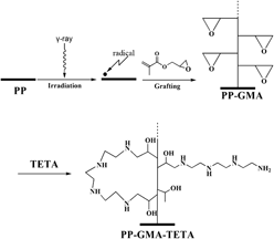
A novel kind of solid amine-containing fibrous adsorbent (PP-GMA-TETA) was prepared through irradiation grafting copolymerization with glycidyl methacrylate (GMA) onto polypropylene (PP) fiber, followed by reacting with triethylenetetramine (TETA) to introduce primary and secondary amine groups on its surface. The effects of the reaction conditions, such as the TETA concentration, temperature, and reaction time on amination degree of PP-GMA-TETA, were investigated. Adsorption capacity of PP-GMA-TETA with 77.7% amination degree could reach 4.72 mmol/g. After adsorption, the spent fiber could be completely regenerated at 100 °C by steam for 20 min and its adsorption behavior kept almost constant within six recycles. The comparison of adsorption capacities of amine fibers aminated with various aminating agents also demonstrated that fibers with higher content of primary amine would obtain faster adsorption rates and higher adsorption capacities.
Besides graphene and hexagonal boron nitride, transition metal dichalcogenides (TMDs) also exhibit a layered structure in which the layers weakly interact via van der Waals forces. Semiconducting TMDs in bulk are indirect band gap materials. However, an isolated sheet exhibits a direct gap. This particular behavior makes them very attractive in terms of optical properties. Moreover, NbS2 and NbSe2 in bulk and their monolayers are metallic. Density functional theory calculations were carried out to study different TMD bilayer systems. First, different bilayer geometries with different stackings were considered. It was found that the indirect and direct band gaps compete; however, the indirect band gap always dominates. Surprisingly, bilayer heterostructures of different TMDs have been found to possess direct band gaps. Finally, heterobilayers composed of one metallic monolayer and a semiconducting layer are predicted as novel metallic van der Waals solids that might find applications in new two-dimensional nanodevices.
A new ternary compound Ho2AlGe3 was synthesized and studied by means of X-ray powder diffraction technique. The powder pattern of Ho2AlGe3 was indexed and refined, giving an orthorhombic structure, space group Pnma (No. 62) with the Y2AlGe3 structure type: a = 6.743 98(8) Å, b = 4.163 73(5) Å, c = 17.5834(2) Å, V = 493.74 Å3, Z = 4, ρx = 7.73 g cm−3, F30 = 202.7 (0.004, 37), and RIR = 1.21.
Veatchite polytypes were properly identified from several localities relying solely on micro powder diffraction data. Diagnostic differences in their respective calculated patterns gave reliable identification results when compared with measured data. This permitted the confirmation of co-existing veatchite-1A and -2M on the same specimen from the Billie Mine, Inyo County, California as flat elongated crystals (-1A) and flat rhombic plates (-2M), respectively. On the specimen from the Sterling Borax Mine (Lang), type-locality for veatchite-2M, the polytype veatchite-1A was confirmed from radiating rhombic plates. From the type specimen for veatchite-1A (rhombic plates), collected from the borate deposit in Emet, Turkey, an additional unknown polytype of this mineral was discovered, but lacks suitable material for a complete characterization. At the Penobsquis deposit near Sussex in New Brunswick, Canada, only veatchite-2M was encountered. The area between 20 and 25°2θ holds the following diffraction signatures: -1A (two sets of double peaks at approximately 21.5 and 24.5°2θ), -1M (single peaks at 20 and 23°2θ) and -2M (double peaks at 20 and 23°2θ). The unknown polytype from Emet, Turkey differs from polytype-1A in that same range by having single peaks at the 21.5 and 24.5° instead of double peaks.
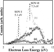
The continuation of Moore's law requires new materials at both extremes of the dielectric permittivity spectrum and an increased understanding of the fundamental mechanisms limiting their electrical reliability. To address the latter, reflection electron energy loss spectroscopy has been utilized to measure the band gap of various oxide-based low and high dielectric constant (k) materials of interest to the semiconductor industry. In situ Ar+ sputtering has been additionally utilized to simulate process-induced defect states that are believed to contribute to electrical leakage, time-dependent dielectric breakdown, charge trapping, and other fixed-charge reliability issues in nano-electronic devices. It is observed that Ar+ sputtering predominantly generates surface oxygen vacancy defects in the upper portion of the band gap for both low and high-k dielectric materials. These results are in agreement with numerous theoretical investigations of defects in low and high-k dielectric materials and models for mechanisms that limit their reliability.
Electron microscopes are proving themselves indispensible tools in the world of nanotechnology. In this brief overview, we explore the potential of electrons within in situ transmission electron microscopy (TEM) with the electrons provided either from the imaging electron beam or from electrical currents across contacted specimens to nanoengineered graphene based on work at our labs. The use of electrons is demonstrated to be enormously versatile to pattern, heal, and even fabricate graphene. In essence, electrons provide a useful engineering tool box that with further development will enable device fabrication and modification inside a TEM, thus allowing one to study structure–property relationships of graphene as well as other low dimensional materials in near real time with atomic precision.
Properties of entangled materials, made of fibers, depend on the number and the nature of contacts between fibers and fibers orientation. Nonsintered and sintered steel wools have been characterized by x-ray tomography to extract structural information such as fibers orientation and number of contacts before and during compression. Image analysis techniques were developed on tomography images and validated on virtual materials, generated and deformed by numerical simulation based on molecular dynamic equations. The structural parameters measured during the structural characterization were finally used to link the structure of the studied material with the measured mechanical properties. To do this link, an analytical model usually used for this kind of material was modified to describe the evolution of mechanical properties in compression.
ZnS/CdS semiconductor composites were synthesized successfully by combining a hydrothermal route with a homogeneous precipitation process. The as-prepared products were characterized by x-ray diffraction, scanning electron microscopy, and energy dispersive x-ray spectrometer. The results showed that the as-prepared products were composed of ZnS microspheres with a face-centered cubic phase and CdS nanoparticles with hexagonal phase, CdS nanoparticles were found to be assembled on the surfaces of the cubic ZnS microspheres. In addition, the ultraviolet-visible absorption spectroscopy and the room temperature photoluminescence (PL) spectroscopy of the ZnS microspheres and ZnS/CdS composites were also investigated. The PL testing indicated that the emission peak of as-prepared ZnS/CdS composites not only exhibited an obvious blue shift but also its intensity had a large enhancement compared to the pure ZnS microspheres. Furthermore, the photocatalytic degradation test showed that the as-prepared ZnS/CdS composites showed excellent photocatalytic degradation activity for methyl orange under UV irradiation. This enhanced activity may be related to the modification of CdS nanoparticles on the surfaces of ZnS microspheres.
Electrical properties of ZrO2 formed by simultaneous oxidation and nitridation of sputtered Zr thin films on Si have been systematically investigated. Various oxidation/nitridation temperatures (500, 700, 900, and 1100 °C) have been carried out in N2O ambient for an extended time of 20 min. Results indicated that the sample oxidized and nitrided at 700 °C possessed the highest effective dielectric constant of 18.22 and electrical breakdown field of 10.7 MV/cm at a current density of 10−6 A/cm2. This is attributed to the lowest effective oxide charge, interface-trap density, and total interface-trap density. The Fowler–Nordheim tunneling mechanism has been investigated for all samples and the highest value of barrier height extracted between the conduction band edges of oxide and semiconductor was 1.22 eV.
In this paper, the effect of the addition of tungsten carbide on the behavior of Fe–WC system during the mechanical alloying (MA) process has been investigated. For this purpose, raw materials containing industrial ferrotungsten and carbon black with a bit of tungsten carbide powder were milled in a high energy ball mill, and sampling was done at different times. An XRD instrument was used for estimating the probable transformation of phases and properties in the milled sample. Microstructures of specimens were studied using electron microscopy. Results showed that MA even at high milling time could not transform raw materials to other materials in a system containing ferrotungsten and carbon black. In samples with primary tungsten carbide, this was synthesized gradually at a milling time of more than 75 h, and finally, the Fe–WC composite was produced as the final product. Crystalline sizes of the synthesized carbide were in nanometer order that was confirmed by transmission electron microscopy images.
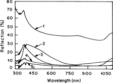
Sol–gel-derived aluminum (Al)-doped zinc oxide thin films have been deposited on silicon (Si) wafers and microslide glass substrates using the spin coating technique. The atomic ratio of Al:Zn in the films is 0.05, 0.1, 0.2, and 0.3. The films have been characterized using different techniques, i.e., x-ray diffraction, Fourier transform infrared spectroscopy, atomic force microscopy, scanning electron microscopy, UV-visible-near infrared spectrophotometry, spectroscopic ellipsometry, and the four-probe method. The films have exhibited excellent optical transmittance (∼90%). The refractive indices of the films are in the range between 1.47 and 1.53. The thickness of the films is in the range of 103–115 nm. The films have demonstrated reflectivity of about 3% at a wave length of 600 nm. The reflectivity, transmittance, refractive index, and thickness values of the films show that the films are promising candidates for utility as antireflection coatings in silicon solar cells.
High quality CdSe nanocrystals (NCs) were synthesized via a nonorganometallic precursor and extracted in different solvents. The difference in the influence of the nature of the solvent namely ethanol, N,N-dimethyl formamide (DMF), and acetonitrile on extraction of the same type of NCs was studied with respect to quality and stability of NCs. Characterization by x-ray diffraction technique, absorption–emission spectroscopy, scanning, transmission, and atomic force microscopy demonstrated the formation of NCs of good optical property and surface composition from the synthesis method used. Different polarities of the solvent strongly influence photoluminescence (PL), surface defects, concentrations of NCs extracted, particle sizes, and surface passivation. Ethanol extraction results in small-sized NCs and good particle size distribution. DMF extraction causes lesser interfacial defects and hence prevents radiative recombinations. PL quenching was observed in all the three solvents, and this necessitates further stabilization of NCs. The stability of the so-extracted NCs was evaluated for change in their properties with respect to aging. Aging substantiated the adverse effects of acetonitrile to extract the lesser surface passivated NCs leading to Ostwald ripening and island formation. The phase and structure of NCs remain unaffected with aging or by the nature of solvent used.
By combining high-resolution transmission electron microscopy and scanning transmission electron microscopy with analytical capability, we investigated the nanostructure of a textured hematite photoanode with columnar grains obtained by the colloidal deposition of magnetite nanocrystals. This initial report describes in detail the structure and chemistry of the α-Fe2O3/SnO2:F interface by identifying semicoherent and incoherent interfaces as well as a localized interdiffusion layer of Sn and Fe at the interface (∼100 nm in length). Our study indicates that unintentional doping by tin at a high sintering temperature is not significant in enhancing hematite photoanode performance for water oxidation. The correlation of nanoscale morphology with photoelectrochemical characterization facilitated the identification of the beneficial effect of a preferential growth direction of a hematite film along the [110] axis for water-splitting efficiency.
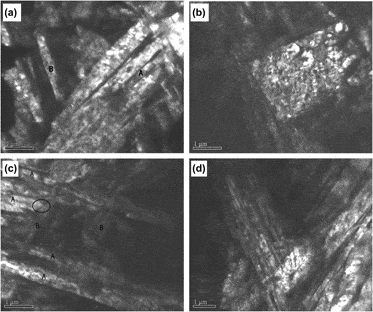
The conventional process for preparing dry spinnable regenerated silk fibroin (RSF) aqueous solution needs not only an addition of Ca2+ but also an adjustment of pH value. In this work, an RSF dry spinning dope was prepared by using a simplified method with solely adding Ca2+. Compared with the conventional RSF solution, the simply prepared aqueous solution showed similar content of β-sheet conformation and diameter of RSF aggregates but lower viscosity. Furthermore, the posttreated RSF fiber dry-spun from this simply prepared solution showed higher crystallinity and crystalline orientation, smaller crystallite size, and better mechanical properties. It could be concluded that Ca2+ played a much more important role than pH value in improving the structures and properties of RSF spinning solution and fibers. Therefore, the step of adjusting pH value could be excluded in the process of preparing high performance RSF fibers.
Dynamic recrystallization (DRX) of 99.9999% aluminum single crystal at room temperature was examined under frictionless deformation mode. To exclude the self-heating of the specimen due to applied high strain, a microcrack that localizes the stress at a very small region was intentionally introduced by controlled local necking. For the in situ observation of DRX, a specially designed in situ microdeformation device was positioned inside an electron backscattered diffraction system chamber. Recrystallized grains showed relatively random texture and preferred growth direction. The subgrains with low-angle grain boundaries formed by dynamic recovery transformed into small grains with high-angle grain boundaries, acting as nuclei for discontinuous dynamic recrystallization and growing by further deformation. The DRX in pure aluminum can take place under frictionless tensile deformation conditions at room temperature, and the stress localization and high purity are key issues for the DRX of aluminum at room temperature.
Using a combination of high-resolution dilatometric measurements and microstructural analysis, this study investigated the bainitic transformation behavior in ultra-high strength 30CrNi3MoV steel after experiencing small deformation at 850 °C (in the nonrecrystallization austenite region). Under the influence of the small deformation in the nonrecrystallization austenite region, the bainite starting temperature (Bs) raised, the bainite finishing temperature (Bf) decreased, granular bainite was promoted to form, and intersections of differently oriented bainite laths became more common in the microstructure. The increase of Bs is owing to the stored energy in distorted austenite grain boundaries, which can serve as an extra mechanical driving force for bainitic transformation during continual cooling. The decrease of Bf can attributed to the more universal intersections of bainite laths with different orientations, which can decelerate the overall growth rate of bainite. The promoted formation of granular bainite is closely related to the increase of Bs because granular bainite usually forms at relatively high temperatures in the bainite range, above upper bainite and lower bainite.
Experimental X-ray powder diffraction data, unit-cell parameters, and space group for levetiracetam, C8H14N2O2, are reported [a = 9.197(5) Å, b = 8.006(0) Å, c = 6.289(3) Å, β = 108.457(3)°, unit-cell volume V = 439.261 Å3, Z = 2, and space group P21]. All measured lines were indexed and are consistent with the P21 space group. No detectable impurity was observed.
Experimental X-ray powder diffraction data, unit-cell parameters and space group for schisanhenol, C23H30O6, are reported [a = 14.6157 Å, b = 12.8801 Å, c = 11.4907 Å, unit-cell volume V = 2163.14 Å3, Z = 4, and space group P212121]. All of the measured lines were indexed and are consistent with the P212121 space group. No detectable impurities were observed.