Refine search
Actions for selected content:
106129 results in Materials Science
QLEDs for displays and solid-state lighting
-
- Journal:
- MRS Bulletin / Volume 38 / Issue 9 / September 2013
- Published online by Cambridge University Press:
- 12 September 2013, pp. 703-711
- Print publication:
- September 2013
-
- Article
- Export citation
A concrete path to sustainability
-
- Journal:
- MRS Bulletin / Volume 38 / Issue 9 / September 2013
- Published online by Cambridge University Press:
- 12 September 2013, pp. 678-679
- Print publication:
- September 2013
-
- Article
-
- You have access
- HTML
- Export citation
Pure colors from core–shell quantum dots
-
- Journal:
- MRS Bulletin / Volume 38 / Issue 9 / September 2013
- Published online by Cambridge University Press:
- 12 September 2013, pp. 696-702
- Print publication:
- September 2013
-
- Article
- Export citation
Universities prepare next-generation workforce to benefit from the Materials Genome Initiative: www.whitehouse.gov/mgi
-
- Journal:
- MRS Bulletin / Volume 38 / Issue 9 / September 2013
- Published online by Cambridge University Press:
- 12 September 2013, pp. 673-674
- Print publication:
- September 2013
-
- Article
-
- You have access
- HTML
- Export citation
Bright and stable quantum dots and their applications in full-color displays
-
- Journal:
- MRS Bulletin / Volume 38 / Issue 9 / September 2013
- Published online by Cambridge University Press:
- 12 September 2013, pp. 712-720
- Print publication:
- September 2013
-
- Article
- Export citation
Crystalline reflectors enable ultralow-thermal-noise optical cavities
-
- Journal:
- MRS Bulletin / Volume 38 / Issue 9 / September 2013
- Published online by Cambridge University Press:
- 12 September 2013, pp. 670-671
- Print publication:
- September 2013
-
- Article
-
- You have access
- HTML
- Export citation
EU and industry join forces to invest €22 billion in research and innovation: http://ec.europa.eu/research/jti/index_en.cfm
-
- Journal:
- MRS Bulletin / Volume 38 / Issue 9 / September 2013
- Published online by Cambridge University Press:
- 12 September 2013, p. 674
- Print publication:
- September 2013
-
- Article
-
- You have access
- HTML
- Export citation
Bruce Clemens teaches materials science online
-
- Journal:
- MRS Bulletin / Volume 38 / Issue 9 / September 2013
- Published online by Cambridge University Press:
- 12 September 2013, pp. 675-676
- Print publication:
- September 2013
-
- Article
-
- You have access
- HTML
- Export citation
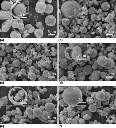
Improvement of luminescence properties of Ca0.8Zn0.2TiO3:Pr3+ prepared by hydrothermal method
-
- Journal:
- Journal of Materials Research / Volume 28 / Issue 18 / 28 September 2013
- Published online by Cambridge University Press:
- 28 August 2013, pp. 2590-2597
- Print publication:
- 28 September 2013
-
- Article
- Export citation
Structure and composition of Au/Co magneto-plasmonic nanoparticles
-
- Journal:
- MRS Communications / Volume 3 / Issue 3 / September 2013
- Published online by Cambridge University Press:
- 28 August 2013, pp. 177-183
- Print publication:
- September 2013
-
- Article
- Export citation

Beam-induced crystallization of amorphous Me–Si–C (Me = Nb or Zr) thin films during transmission electron microscopy
-
- Journal:
- MRS Communications / Volume 3 / Issue 3 / September 2013
- Published online by Cambridge University Press:
- 28 August 2013, pp. 151-155
- Print publication:
- September 2013
-
- Article
- Export citation
Fine-sized BaSi3Al3O4N5:Eu2+ phosphors prepared by solid-state reaction using BaF2 flux
-
- Journal:
- Journal of Materials Research / Volume 28 / Issue 18 / 28 September 2013
- Published online by Cambridge University Press:
- 28 August 2013, pp. 2598-2604
- Print publication:
- 28 September 2013
-
- Article
- Export citation

Effect of MoO3 addition on the microstructure and mechanical properties of Ti2A1C prepared by reactive hot pressing
-
- Journal:
- Journal of Materials Research / Volume 28 / Issue 16 / 28 August 2013
- Published online by Cambridge University Press:
- 27 August 2013, pp. 2164-2170
- Print publication:
- 28 August 2013
-
- Article
- Export citation

Thin film cathodes in SOFC research: How to identify oxygen reduction pathways?
-
- Journal:
- Journal of Materials Research / Volume 28 / Issue 16 / 28 August 2013
- Published online by Cambridge University Press:
- 27 August 2013, pp. 2085-2105
- Print publication:
- 28 August 2013
-
- Article
- Export citation
JMR volume 28 issue 16 Cover and Front matter
-
- Journal:
- Journal of Materials Research / Volume 28 / Issue 16 / 28 August 2013
- Published online by Cambridge University Press:
- 27 August 2013, pp. f1-f4
- Print publication:
- 28 August 2013
-
- Article
-
- You have access
- Export citation
JMR volume 28 issue 16 Cover and Back matter
-
- Journal:
- Journal of Materials Research / Volume 28 / Issue 16 / 28 August 2013
- Published online by Cambridge University Press:
- 27 August 2013, pp. b1-b4
- Print publication:
- 28 August 2013
-
- Article
-
- You have access
- Export citation
Structural characterization of a new acentric protonated garnet: Li6−xHxCaLa2Nb2O12
-
- Journal:
- Journal of Materials Research / Volume 28 / Issue 16 / 28 August 2013
- Published online by Cambridge University Press:
- 27 August 2013, pp. 2147-2153
- Print publication:
- 28 August 2013
-
- Article
- Export citation
-
A new acentric protonated garnet Li6−xHxCaLa2Nb2O12 has been synthesized and structurally characterized from Rietveld refinement of high-resolution neutron diffraction data. This phase can be prepared by Li+/H+ exchange on the mother garnet Li6CaLa2Nb2O12 in acetic acid heated at reflux for 4 days, conditions determined after several tests varying acid solution, time, and temperature. Li6−xHxCaLa2Nb2O12 crystallizes in the noncentrosymmetric cubic space group I $\overline 4$3d (no. 220) with the cell parameter a = 12.8040(3) Å. The noncentrosymmetry has been confirmed from unambiguous results obtained by second harmonic generation test as well as from transmission electron microscopy study (selected area electron diffraction). The Li+/H+ exchange corresponds to a topotactic reaction since this new protonated phase is built from the garnet framework [CaLa2Nb2O12]6− like its mother form Li6CaLa2Nb2O12 with lithium and proton cations distributed on different sites.

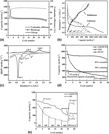
Ultrathin NiO nanoflakes perpendicularly oriented on carbon nanotubes as lithium ion battery anode
-
- Journal:
- Journal of Materials Research / Volume 28 / Issue 18 / 28 September 2013
- Published online by Cambridge University Press:
- 20 August 2013, pp. 2577-2583
- Print publication:
- 28 September 2013
-
- Article
- Export citation

Unusual oxidation behavior of light metal hydride by tetrahydrofuran solvent molecules confined in ordered mesoporous carbon
-
- Journal:
- Journal of Materials Research / Volume 29 / Issue 1 / 14 January 2014
- Published online by Cambridge University Press:
- 20 August 2013, pp. 55-63
- Print publication:
- 14 January 2014
-
- Article
- Export citation
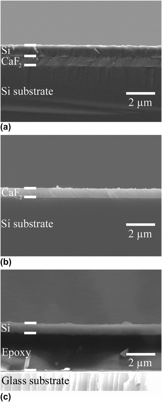
Rapid liftoff of epitaxial thin films
-
- Journal:
- Journal of Materials Research / Volume 28 / Issue 18 / 28 September 2013
- Published online by Cambridge University Press:
- 20 August 2013, pp. 2564-2569
- Print publication:
- 28 September 2013
-
- Article
- Export citation
