To save content items to your account,
please confirm that you agree to abide by our usage policies.
If this is the first time you use this feature, you will be asked to authorise Cambridge Core to connect with your account.
Find out more about saving content to .
To save content items to your Kindle, first ensure no-reply@cambridge.org
is added to your Approved Personal Document E-mail List under your Personal Document Settings
on the Manage Your Content and Devices page of your Amazon account. Then enter the ‘name’ part
of your Kindle email address below.
Find out more about saving to your Kindle.
Note you can select to save to either the @free.kindle.com or @kindle.com variations.
‘@free.kindle.com’ emails are free but can only be saved to your device when it is connected to wi-fi.
‘@kindle.com’ emails can be delivered even when you are not connected to wi-fi, but note that service fees apply.
Within the last decade, inkjet printing technology has developed from only a text and graphic industry to a major topic of scientific research and development. Inkjet printing can be used as a highly reproducible noncontact patterning technique to print at high speeds either small or large areas with high quality features; it requires only small amounts of functional materials, which immediately lower production costs. Furthermore, inkjet printing reduces the amount of processing steps due to its additive technique of materials deposition, which further decreases productions costs. This contribution provides a literature survey covering the latest results in low temperature sintering inkjet-printed metal precursor materials in a fast and efficient manner, aiming for roll-to-roll processing. The prepared features can be used as interconnects and contacts for microelectronic applications, including organic light-emitting diodes, organic photovoltaics, and radio frequency identification tags.
Nitrogen-vacancy (NV) color centers in diamond are currently considered excellent solid-state magnetic field sensors. Their long coherence times at room temperature and their atomic size allow for achieving both high magnetic field sensitivity and nanoscale spatial resolution in ambient conditions. This article reviews recent progress in magnetic field imaging with NV centers. We focus on two topics: scanning probe techniques with single NV centers and their application in the imaging of nanoscale magnetic structures, as well as recent development of magnetometers with ensembles of NV centers, which image magnetic fields at micron-length scales with extremely high sensitivities.
Many studies have been carried out to thoroughly understand the colorization mechanisms of bird feathers. However, most of the methods used so far are time-consuming (in days) and involve rather complicated steps (5 to 12). Here, we report a rapid way of producing ‘PbS bird feathers’; this method is inspired by a hair-dyeing method used in ancient Egypt 4000 years ago. The complete synthesis route comprises only two steps and can be completed within 2 h, with the original morphologies of bird feathers well preserved. This method has potential to be extended to the fast fabrication of other functional sulfides which are too complicated to fabricate otherwise.
This article describes the multifunctional applications of TiO2. It substantiates the universality of the anodization process to grow well-ordered TiOxnanotube (T–NT) of hollow cylindrical shape on a variety of planar and nonplanar substrates. It highlights an approach to effectively bring down the cost of anodization via utilization of a small volume of electrolyte. The multifunctionality of these nanostructures is highlighted through representative examples that illustrate wide ranging optical, electronic, and catalytic properties. Combining the T–NT with other materials such as metals and photoactive additives to form composite nanostructures has been shown to benefit photocatalysis, photovoltaics, biological processes, and environment-related applications. This article also demonstrates the applicability of T–NT as an agent to produce dissolved oxygen in simulated blood—an application that can assist in the development of artificial lungs. Key results from the research group, collaborations, and recent articles are highlighted.
A whisker and hillock growth model based on local film microstructure, grain misorientation, and elastic strain energy density (ESED) as the driving force for growth was developed to predict preferred sites for growth. Local grain orientations and strains measured by synchrotron microdiffraction in nine regions containing whiskers or hillocks were compared with elastic finite element analysis simulations including Sn elastic anisotropy. Whisker and hillock grains were observed to have higher crystallographic misorientations with neighboring grains than generally observed in the microstructure. While elastic simulations predicted higher local out-of-plane elastic strains and ESEDs at those locations with high misorientations before growth, synchrotron measurements of out-of-plane strains of whisker and hillock grains after growth showed relaxation, with correspondingly low ESEDs calculated from measured strains. Hence, highly localized out-of-plane elastic strains and ESEDs of grains with high relative misorientations with their neighbors determined, at least in part, which grains became whiskers or hillocks.
We report an alternative interruption scheme to effectively improve the abruptness of GaN/AlGaN superlattices by minimizing the asymmetric feature of different types of heterointerfaces. It is found by x-ray diffraction that the interface abruptness is degraded and the GaN thickness is reduced with the interruption time increasing. Detailed investigation with scanning transmission electron microscopy demonstrates that the Al diffusion and the interface etching effect at the GaN/AlGaN interface are the critical reasons leading to the interfacial asymmetry. An alternative interface–interruption scheme is then proposed to enhance the abruptness of the superlattice interfaces, and consequently, the emission efficiency can also be significantly enhanced.
In this article, ZnO microtube was prepared using mixed powder of Zn, ZnO, and carbon as source via chemical vapor deposition method. The growth process was discussed in detail, and the high Zn vapor pressure and high growth temperature were considered as two crucial factors determining the formation of tubular structure. A two-step growth model was proposed, namely initial deficient-oxidation and followed by second-volatilization. Four another experiments were further conducted to analyze the growth behavior of reagent species under different Zn vapor pressure and growth temperature, respectively. These experimental results indicated that the formation of Zn-rich structure under enough high Zn vapor pressure and second-volatilization of these abundant interstitial Zn under high growth temperature were important to form tubular structure. Our experimental method provided a feasible route to prepare other hollow structures, such as oxide, sulfide, etc. Furthermore, these synthesized ZnO microtube might have potential application as functional blocks in nanodevices.
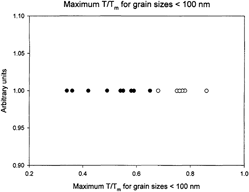
Data from the literature and our laboratory have been reviewed regarding the maximum homologous temperatures that can be attained by the addition of solute elements that may induce thermodynamic or kinetic (Zener pinning) stabilization of a nanocrystalline grain size (<100 nm) to elevated temperatures. The results of this review suggest that kinetic stabilization by Zener pinning by nanoscale second phases may be the more effective strategy for keeping a nanoscale grain microstructure at the highest homologous temperatures. More research is necessary to confirm this suggestion and to determine the influence of nanoscale grain boundary second phases on the mechanical behavior of the nanocrystalline matrix.
We describe the synthesis and fabrication of a graphene oxide (GO) and single-walled carbon nanotube (SWCNT) composite ink (GO–SWCNT ink) for electrochemically stable supercapacitors. Atomic force microscopy and scanning electron microscopy studies demonstrate that the obtained GO flakes are single layer with size distribution from 100 nm to 20 μm. SWCNTs are dispersed using a GO aqueous solution (2 mg/mL) with sonication support to achieve a SWCNT concentration of 12 mg/mL, the highest reported value so far without surfactant assistance. Raman spectroscopy studies indicate that the full-width at half-maximum of the G band increases with the mixing of SWCNT and GO indicating that electronic structure changes via π–π interactions of GO sheets and SWCNTs. Paper-based electrodes of supercapacitor were conveniently fabricated with GO–SWCNT composite ink via a dip casting method. By using different concentrations of SWCNT in the ink, the paper electrodes provide different capacitance values. The highest value of specific capacitance reaches 295 F/g at a current density of 0.5 A/g with a GO/SWCNT weight ratio of 1:5. The cycling stability for the GO–SWCNT paper electrode supercapacitors indicates capacitance retention of 85% over 60,000 cycles.
Stable, aqueous, red-to-near infrared emission is critical for the use of silicon nanoparticles (Si NPs) in biological fluorescence assays, but such Si NPs have been difficult to attain. We report a synthesis and surface modification strategy that protects Si NPs and preserves red photoluminescence (PL) in water for more than 6 mo. The Si NPs were synthesized via high temperature reaction, liberated from an oxide matrix, and functionalized via hydrosilylation to yield hydrophobic particles. The hydrophobic Si NPs were phase transferred to water using the surfactant cetyltrimethylammonium bromide (CTAB) with retention of red PL. CTAB apparently serves a double role in providing stable, aqueous, red-emitting Si NPs by (i) forming a hydrophobic barrier between the Si NPs and water and (ii) providing aqueous colloidal stability via the polar head group. We demonstrate preservation of the aqueous red emission of these Si NPs in biological media and examine the effects of pH on emission color.
Oxygen-free high conducting copper wires drawn to true strains of 2.3, 3.1, and 3.6 exhibit inhomogeneity in the form of three distinct concentric regimes: the inner core, the midsection, and the outer region. While the microtexture of the inner core was dominated by a strong <111> + weak <100> duplex fiber texture, the midsection and the outer region had a comparatively weaker texture. An upper bound plasticity modeling and the nanohardness measurement revealed that the midsection was the most strained region. Upon annealing at 170 °C, the 2.3-strained wire did not recrystallize, whereas the 3.1- and 3.6-strained wires exhibited partial recrystallization. For the 3.6 wire, the inner core was unrecrystallized, while the midsection and outer region recrystallized with strong <100> + weak <111> fiber texture. The recrystallized grains were classified as type “A” grains, which grew laterally with <100>//DD orientation, and type “B” grains, which generally grew axially with <111>//DD orientation.
We have studied the atomic ordering of B-site transition metals and magnetic properties in the pulsed laser deposited films of La2CrFeO6 (LCFO) and La2VMnO6 (LVMO), whose bulk materials are known to be single perovskites with random distribution of the B-site cations. Despite similar ionic characters of constituent transition metals in each compound, the maximum B-site order attained was surprisingly high, ∼90% for LCFO and ∼80% for LVMO, suggesting a significant role of epitaxial stabilization in the spontaneous ordering process. Magnetization and valence state characterizations revealed that the magnetic ground state of both compounds was coincidently ferrimagnetic with saturation magnetization of ∼2 μB per formula unit, unlike those predicted theoretically. In addition, they were found to be insulating with optical band gaps of 1.6 and 0.9 eV for LCFO and LVMO, respectively. Our results present a wide opportunity to explore novel magnetic properties of binary transition metal perovskites upon epitaxial stabilization of the ordered phase.
We analyze the effect of postdeposition annealing conditions on both the structure and the created defects in Zn0.90Co0.10O thin films, which deposited on the Si(100) substrates by the radio frequency magnetron sputtering technique using a homemade target. The dependence of the number and distribution of defects in homogeneously substituted Co+2 for Zn+2 ions in ZnO lattice on the annealing conditions is investigated. Orientations of thin films are in the [0002] direction with a surface roughness changing from 67 ± 2 nm to 25.8 ± 0.6 nm by annealing. The Co+2 ion substitution, changing from 7.5% ± 0.3% to 8.8 ± 0.3%, leads to the formation of Zn–O–Co bonds instead of Zn–O–Zn bonds and splitting of the Co 2p energy level to Co 2p1/2 and Co 2p3/2 with an energy difference of 15.67 ± 0.06 eV. The defects in the lattice are revealed from the correlations between Zn–O–Co bonds and intensity of the Raman peak at around 691 cm−1. In addition, the asymmetry changes of O 1s peak positions in the x-ray photoelectron spectra are in agreement with the Raman results.
Due to its excellent physical properties, graphene acting as reinforcing fillers has attracted intense interests. To achieve a controlled distribution, the formation of a conductive network composed of graphene sheets within polymer matrix is of critical importance. In this work, polystyrene (PS) microspheres wrapped by graphene oxide (GO) sheets were prepared via layer-by-layer (LBL) assembly of oppositely charged GO sheets onto PS microspheres. The deposited GO was then reduced, and the composite films with a graphene conductive network were prepared by hot pressing. The morphology of graphene conductive network was studied, and the thermal and electrical properties of the composite films were measured. The as-prepared composites showed an improved thermal stability as well as electrical conductivity with a percolation threshold as low as 0.2 vol%. The combination of latex technology and LBL self-assembly method thus demonstrated an efficient and facile approach to fabricate electrically conductive graphene/polymer composites.