To save content items to your account,
please confirm that you agree to abide by our usage policies.
If this is the first time you use this feature, you will be asked to authorise Cambridge Core to connect with your account.
Find out more about saving content to .
To save content items to your Kindle, first ensure no-reply@cambridge.org
is added to your Approved Personal Document E-mail List under your Personal Document Settings
on the Manage Your Content and Devices page of your Amazon account. Then enter the ‘name’ part
of your Kindle email address below.
Find out more about saving to your Kindle.
Note you can select to save to either the @free.kindle.com or @kindle.com variations.
‘@free.kindle.com’ emails are free but can only be saved to your device when it is connected to wi-fi.
‘@kindle.com’ emails can be delivered even when you are not connected to wi-fi, but note that service fees apply.
By
F. M. Izrailev, Universidad Autónoma de Puebla, Apdo. Post. J-48, Puebla 72570, México,
N. M. Makarov, Universidad Autónoma de Puebla, Priv. 17 Norte No. 3417, Col. San Miguel Hueyotlipan, Puebla 72050, México
In recent years, increasing attention has been paid to the so-called correlated disorder in low-dimensional disordered systems. Interest in this subject is mainly due to two reasons. First, it was found that specific correlations in a disordered potential can result in quite unexpected anomalous properties of scattering. Second, it was shown that such correlations can be relatively easily constructed experimentally, at least in the one-dimensional Anderson model and in Kronig–Penney models of various types. Therefore, it seems to be feasible to fabricate random structures with desired scattering properties, in particular when one needs to suppress or enhance the localization in given frequency windows for scattering electrons or electromagnetic waves. In addition, it was understood that, in many real systems, correlated disorder is an intrinsic property of the underlying structures. One of the most important examples is a DNA chain, for which strong correlations in the potential have been shown to manifest themselves in an anomalous conductance. Thus, the subject of correlated disorder is important both from the theoretical viewpoint, and for various applications in physics.
The key point of the theory of correlated disorder is that the localization length for eigenstates in one-dimensional models absorbs the main effect of correlations in disordered potentials. This fact has been known since the earliest analytical studies of transport in continuous random potentials. However, until recently the main interest was in delta-correlated potentials, or in potentials with a Gaussian-type of correlation.
Cloaking is the ability to make a region of space, and everything in it, invisible to an external observer. It has been the dream of fantasy writers for decades. In 2009, John Mullan [1] of The Guardian newspaper summarized the ten most important works that use the theme: The Invisible Man by H. G. Wells, The Republic by Plato, The Lord of the Rings by J. R. R. Tolkien, the Harry Potter books by J. K. Rowling, Theogony by Hesiod, Dr Faustus by Christopher Marlowe, The Tempest by William Shakespeare, The Voyage of the Dawn Treader by C. S. Lewis, The Emperor's New Clothes by Hans Christian Andersen, and The Hitchhiker's Guide to the Galaxy by Douglas Adams. A true cloak allows the clear observation of the space behind the cloaked region, and the cloaked region casts no shadow and produces no wavefront changes in the light that has passed through the cloaked region. It is not possible to build a perfect invisibility cloak, as was perceptively observed in the Star Trek series in which cloaked Romulan and Klingon spaceships could be detected by the subtle disturbances of space that the cloak produced.
Interest in making real cloaking devices can be traced to two seminal articles, one by John Pendry and his co-workers [2], and the other by Ulf Leonhardt [3]. Their approach can be called the transformational optics approach to cloaking, which will be discussed in more detail later.
By
Evgeny Popov, Aix-Marseille Université, CNRS, Unité Mixte de Recherche 6133, Domaine Universitaire de Saint Jerome, 13397 Marseille Cedex 20, France,
Nicolas Bonod, Aix-Marseille Université, CNRS, Unité Mixte de Recherche 6133, Domaine Universitaire de Saint Jerome, 13397 Marseille Cedex 20, France
A brief reminder of the history of grating anomalies and plasmon surface waves
The recent history of the research and development around plasmon surface waves that was initiated by the work published in Nature in 1998 by Ebbesen et al. [1] looks like a ten-fold compressed version of studies initiated more than a century ago by Robert Wood with his discovery of anomalies in the efficiency of metallic diffraction gratings, now known as Wood's anomalies [2]. In 1902, R. Wood wrote: “I was astounded to find that under certain conditions, the drop from maximum illumination to minimum, a drop certainly from 10 to 1, occurred within a range of wavelengths not greater than the distance between the sodium lines,” an observation that marked the discovery of grating anomalies.
The first period of the search for their explanation is marked by the attempt of Lord Rayleigh [3, 4] to link Wood's anomalies to the redistribution of the energy due to the passing-off (cut-off) of higher diffraction orders of the grating (transfer from propagating into evanescent type). As pointed out by Maystre [5], his prediction was all the more remarkable as the author first ignored the groove frequency of the grating used by Wood, and thus could not verify this assumption with experimental data.
In recent years it has emerged that planar metamaterials offer a vast range of custom-designed electromagnetic functionalities. The best known are wire grid polarizers, which are established standard components for microwaves, terahertz waves, and the far-infrared. They are expected to be of increasing importance also for the near-infrared [1] and visible light [2]. Equally well developed are frequency selective surfaces [3–6], which are used as filters in radar systems, antenna technology [7], broadband communications, and terahertz technology [8, 9]. However, the range of optical effects observable in planar metamaterials and the variety of potential applications have only become clear since metamaterials research took off in 2000 [10]. Wave plate [11, 12] as well as polarization rotator and circular polarizer [13–15] functionalities have been demonstrated in metamaterials of essentially zero thickness. Traditionally, such components are large as they rely on integrating weak effects over thick functional materials. Polarization rotation has also been seen at planar chiral diffraction gratings [16, 17] and thin layered stereometamaterials [18, 19]. Electromagnetically induced transparency (EIT) [20–24] and high quality factor resonances [20] have been observed at planar structured interfaces. And finally, new fundamental electromagnetic effects leading to directionally asymmetric transmission of circularly [25–29] and linearly polarized waves have been discovered in planar metamaterials.
Planar metamaterials derive their properties from artificial structuring rather than atomic or molecular resonances, and therefore appropriately scaled versions of such structures will show similar properties for radio waves, microwaves, terahertz waves, and, to some extent, in the infrared and optical spectral regions where losses are becoming more important.
By
Peter B. Catrysse, Stanford University, Stanford, CA 94305, USA,
Hocheol Shin, Stanford University, Stanford, CA 94305, USA,
Shanhui Fan, Stanford University, Stanford, CA 94305, USA
All-angle negative refraction of electromagnetic waves [1, 2] has generated great interest because it provides the foundation for a wide range of new electromagnetic effects and applications, including subwavelength image formation [2] and a negative Doppler shift [1], as well as novel guiding, localization and nonlinear phenomena [3, 4]. There has been tremendous progress in achieving negative refraction in recent years using either dielectric photonic crystals [5–9] or metallic meta-materials [10–17]. For either approach, however, there is an underlying physical length scale that sets a fundamental limit [18]. Below such a length scale, the concept of an effective index no longer holds. For photonic crystals, it is the periodicity, which is smaller than but comparable to the operating wavelength of light [8]. For metallic meta-materials, it is the size of each individual resonant element. In the microwave wavelength range, constructing resonant elements that are far smaller than the operating wavelength is relatively straightforward. As one pushes towards shorter optical wavelengths, however, it becomes progressively more difficult to construct resonant elements at a deep subwavelength scale [15]. Moreover, in the optical wavelength range, the plasmonic effects of metals become prominent. The strong magnetic response of metallic structures, as observed in microwave and infrared wavelength ranges, may be fundamentally affected. It is therefore very desirable to accomplish all-angle negative refraction using structures that are flat at an atomic scale.
Negative refraction (NR) has been theoretically predicted [1, 2] and experimentally realized [3–7] in three types of materials. One is a material with a simultaneously negative permittivity and permeability [8–12], leading to a negative refractive index for the medium. The second consists of a photonic crystal (PhC) [13–21], which is a periodic arrangement of scatterers in which the group and phase velocities can be in different directions leading to NR. The third is the indefinite medium [22–28], whose permittivity and/or permeability tensor is an indefinite matrix. In all cases, the bulk properties of the medium, which is inherently inhomogeneous at a subwavelength scale, can be described as having an effective negative refractive index. The active research in these artificial materials has opened doors to a plethora of unusual electromagnetic properties and new applications such as a perfect lens [29], subwavelength imaging [30], cloaking [31], slow light, and optical data storage [32, 33], that cannot be obtained with naturally occurring materials. The holy grail of manufacturing these artificial photonic metamaterial structures is to manipulate light at the nanoscale level for optical information processing and high-resolution imaging.
In order to achieve NR, engineering the bulk electromagnetic properties is normally needed such that the group velocity and phase velocity be at an obtuse angle or even anti-parallel to each other. However, refraction is a surface phenomenon. A bulk-engineered material will have certain inherent surface properties. Negative refraction can be realized in positive index materials by special orientation or by engineering the interface properties.
By
A. I. Fernández-Domínguez, Universidad Autonoma de Madrid, E-28049 Madrid, Spain,
F. García-Vidal, Universidad Autonoma de Madrid, E-28049 Madrid, Spain,
L. Martín-Moreno, Universidad de Zaragoza, E-500009 Zaragoza, Spain
The ability to localize electromagnetic energy below the diffraction limit of classical optics featured by surface plasmon polaritons (SPPs) (electromagnetic surface waves sustained at the interface between a conductor and a dielectric) is currently being exploited in numerous studies ranging from photonics, optoelectronics, and materials science to biological imaging and biomedicine [1]. While the basic physics of SPPs has been described in a number of seminal papers spanning the twentieth century [2, 3], the more recent emergence of powerful nanofabrication and characterization tools has catalyzed a vast interest in their study and exploitation. The dedicated field of plasmonics [4] brings together researchers and technologists from a variety of disciplines, with the common aim to take advantage of the subwavelength light confinement associated with the excitation of SPPs.
Most interest is focused on the optical regime, where SPPs are strongly confined to the respective metal/dielectric interface, i.e. where subwavelength mode localization is achieved in the direction perpendicular to the interface. These strongly confined SPPs occur at frequencies which are still an appreciable fraction of the intrinsic plasma frequency of the metal in question. In this regime, the motion of the conduction electrons at the interface is dephased with respect to the driving electromagnetic fields, leading to a reduction in both phase and group velocities of the SPP, and, therefore, to strong localization. A considerable fraction of the SPP field energy resides inside the conductor.
Nanotechnology has seen enormous progress in recent years, and various techniques are now available for the realization of ordered periodic arrays of particles with nanoscale dimensions. Electron-beam [1] and interference lithography [2], polymer-based nanofabrication [3], and self-assembly techniques [4] indeed enable producing ordered one-dimensional (1-D), two-dimensional (2-D), and even three-dimensional (3-D) arrays of metallic or dielectric nanoparticles with sizes much smaller than the wavelength of operation. As is well established in the field of optical metamaterials, such arrays may interact with light in anomalous and exotic ways, provided that their unit cells are sufficiently close to the individual or collective resonance of these arrays.
The electromagnetic response of optical metamaterials and metasurfaces is very distinct from that of gratings and photonic crystals. In photonic crystals, for which lattice periods are comparable to the wavelength of operation, it is possible to tailor the optical interaction operating near the Bragg collective resonances and Wood's anomalies associated with their period, whereas in optical metamaterials and metasurfaces, we operate near the plasmonic resonances of the individual inclusions, leading to the advantage of a much broader response in terms of the angle of incidence, and the absence of grating lobes in the visible angular spectrum. On the other hand, unlike photonic crystals, optical metamaterials and metasurfaces require a much smaller scale for their unit cells. Moreover, plasmonic materials, required to support the required resonances at the nanoscale, are usually characterized by intrinsic non-negligible loss and absorption.
If a metamaterial can be defined as a deliberately structured material that possesses physical properties that are not possible in naturally occurring materials, then deliberately structured surfaces that possess desirable optical properties that planar surfaces do not posses can surely be considered to be optical metamaterials. The surface structures displaying these properties can be periodic, deterministic but not periodic, or random.
In recent years interest has arisen in optical science in the study of such surfaces and the optical phenomena to which they give rise. A wide variety of these phenomena have been predicted theoretically and observed experimentally. They can be divided roughly into those in which volume electromagnetic waves participate and those in which surface electromagnetic waves participate. Both types of optical phenomena and the surface structures that produce them are described in this volume.
The first several chapters are devoted to optical interactions of volume electromagnetic waves with structured surfaces. One of the earliest examples of a structured surface that acts as an optical metamaterial, and the one that today is perhaps the best known and most widely studied, is a metal film pierced by a two-dimensional periodic array of holes with subwavelength diameters. It was shown experimentally by Ebbesen et al. [1] that the transmission of p-polarized light through this structure can be extraordinarily high at the wavelengths of the surface plasmon polaritons supported by the film.
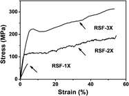
Regenerated silk fibroin (RSF) fibers were directly dry-spun from RSF aqueous solutions into air. To improve mechanical properties of fiber, the as-spun fibers were postdrawn in 80 vol.% ethanol aqueous solution, in which an immersion process was performed subsequently. With the increase in draw ratio, the fibers show substantial improvements of orientation and mechanical properties. Quantitative analysis of Fourier transform infrared spectroscopy indicates that the ratio of β-sheet to α-helix conformation increases sharply at the beginning of immersion process, then approaches a constant value after 90 min of immersion. All fibers exhibit very smooth surfaces. There is no obvious relationship between the pH of the spinning dope and the mechanical properties of the regenerated fibers. The breaking stress of the posttreated fiber is improved up to 301 MPa, which approaches that of degummed silk. The posttreated fiber is over three times the breaking energy of degummed silk.
Bi1.95La1.05TiNbO9 (BLTN-1.05) thin films were prepared on fused quartz substrates by pulsed laser deposition. The x-ray diffraction (XRD) analysis and atomic force microscope (AFM) surface morphology measurements were performed on the samples. The XRD pattern demonstrated that the films are single-phase perovskite structured and well crystallized. The AFM analysis indicated that the films have less rough surface. The fundamental optical constants were obtained through optical transmittance measurements. The nonlinear optical properties of BLTN thin films were measured by a single beam Z-scan technique under 1064 nm excitation. The real and imaginary parts of the third-order nonlinear optical susceptibility χ(3) of the film were measured to be 9.56 × 10⁻⁹ and −3.67 × 10⁻⁹ esu, respectively. The Z-scan results show that BLTN thin films have potential applications in nonlinear optics.
We report the results of an investigation on the structural evolution of a potential new thermoelectric material, Cu3SbSe3, as a function of temperature from 25 to 390 °C. From high-temperature x-ray diffraction data, the refined lattice parameters were seen to change nonlinearly, but continuously, with temperature, with an increased rate of thermal expansion in the a and b lattice parameters from around 125 °C to 175 °C and negative thermal expansion in the c axis from around 100 °C to 175 °C. Crystallographic charge flipping analysis indicated an increase in the disorder of the copper cations with temperature. This reversible order/disorder phase transition in Cu3SbSe3 affects the transport properties, as evidenced by thermal conductivity measurements, which change from negative to positive slope at the transition temperature. This structural change in Cu3SbSe3 has implications for its potential use in thermoelectric generators.
Nanocrystalline silicon thin films were fabricated using a vacuum arc discharge technique. These thin films can be deposited on plastic substrates effectively when cooled by a cryogenic substrate holder. We used single crystal silicon wafers as both the electrodes to ignite the vacuum arc and the silicon ion source to deposit thin films. This resulted in nanocrystalline silicon clusters embedded in the amorphous silicon matrix. This thin film has highly crystalline volume (≈87%), which enhanced the absorption in wide range of wavelengths. Without ion implantation, the in situ doping of p- or n-type thin films can also be achieved. This thin film deposition process has its potential for fabricating thin film transistors and photovoltaic cells on plastic substrates at fairly low production costs.
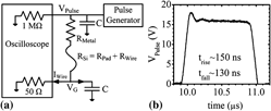
We describe experiments on self-heating and melting of nanocrystalline silicon microwires using single high-amplitude microsecond voltage pulses, which result in growth of large single-crystal domains upon resolidification. Extremely high current densities (>20 MA/cm2) and consequent high temperatures (1700 K) and temperature gradients (1 K/nm) along the microwires give rise to strong thermoelectric effects. The thermoelectric effects are characterized through capture and analysis of light emission from the self-heated wires biased with lower magnitude direct current/alternating current voltages. The hottest spot on the wires consistently appears closer to the lower potential end for n-type microwires and to the higher potential end for p-type microwires. The experimental light emission profiles are used to verify the mathematical models and material parameters used for the simulations. Good agreement between experimental and simulated profiles indicates that these models can be used to predict and design optimum geometry and bias conditions for current-induced crystallization of microstructures.
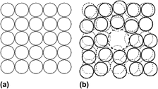
We propose a phenomenological Landau theory to describe polymorphic melting in binary solid solutions. We use the mean atomic displacement as the primary order parameter to represent the loss of the long-range order and the elastic strain induced by alloy component as the secondary order parameter. Under polymorphic constraint where alloy concentration fluctuation is restricted, the model predicts the melting line, also called T0-curve that is depressed by two factors, the static strain field caused by the solute, and the anharmonicity induced by the thermal vibration. We also obtain other thermodynamic properties at and around the melting point. The results confirm well with available experimental results for dilute solutions. We extrapolate the melting line to high concentration region for which no experimental data are available. From the results, we discuss the relation between polymorphic melting and glass transition, as well as glass formability.