To save content items to your account,
please confirm that you agree to abide by our usage policies.
If this is the first time you use this feature, you will be asked to authorise Cambridge Core to connect with your account.
Find out more about saving content to .
To save content items to your Kindle, first ensure no-reply@cambridge.org
is added to your Approved Personal Document E-mail List under your Personal Document Settings
on the Manage Your Content and Devices page of your Amazon account. Then enter the ‘name’ part
of your Kindle email address below.
Find out more about saving to your Kindle.
Note you can select to save to either the @free.kindle.com or @kindle.com variations.
‘@free.kindle.com’ emails are free but can only be saved to your device when it is connected to wi-fi.
‘@kindle.com’ emails can be delivered even when you are not connected to wi-fi, but note that service fees apply.
Moore’s law of transistor scaling, the exponential increase in the number of complementary metal oxide semiconductor (CMOS) transistors per unit area, continues unabated; however, computer clock speeds have remained frozen since 2003. The development of a new digital switch, the piezoelectronic transistor (PET), is designed to circumvent the speed and power limitations of the CMOS transistor. The PET operates on a novel principle: an electrical input is transduced into an acoustic pulse by a piezoelectric element which, in turn, is used to drive a continuous insulator-to-metal transition in a piezoresistive element, thus switching on the device. Performance is enabled by the use of key high response materials, a relaxor piezoelectric, and a rare-earth chalcogenide piezoresistor. Theory and simulation predict, using bulk material properties, that PETs can operate at one-tenth the present voltage of CMOS technology and consuming 100 times less power while running at multi-GHz clock speeds. A program to fabricate prototype PET devices is under way.
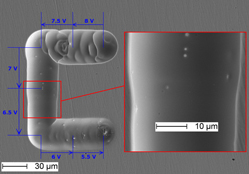
A new technique for micropatterning Fe-based bulk metallic glass surfaces is reported. The transpassive dissolution process is utilized for a defined localized material removal when using a pulsed electrochemical micromachining process. By applying submicrosecond pulses between a work piece and a tool electrode, microholes of high aspect ratio and depth of up to 100 μm can be machined into the bulk glassy Fe65.5Cr4Mo4Ga4P12C5B5.5 alloy. Two potential electrolytes are identified for the machining process. For these electrolytes, different reaction mechanisms are discussed. The possibility of machining more complex structures is demonstrated for the most promising electrolyte, a methanolic H2SO4solution. The impact of the process parameters, pulse length and pulse voltage, on the machining gap and the surface quality of the machined structures is evaluated.
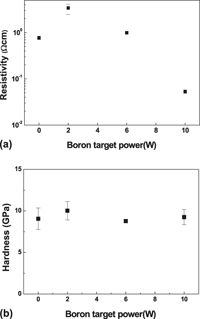
Nitrogen (N) and boron (B) codoped diamond-like carbon (DLC) films were prepared on silicon oxide substrates by RF magnetron sputtering to optimize the electrical conductivity and hardness of DLC film. The electrical conductivity and hardness of the N–B codoped DLC films were controlled simultaneously by varying N2 flow rate with fixed B target power and varying B target power with fixed N2flow rate. The electrical resistivity of the B-doped DLC films showed a cup-shaped relationship with B target power and a U-shaped relationship with the N–B codoped DLC film. However, hardness of the B-doped DLC films showed a decreasing behavior but it was maintained almost constant for the N–B codoped DLC film. These particular electrical and hardness behaviors of the N–B codoped DLC films could be explained by a neutralization effect of N and B codoping.
Concentrated electric field is crucial in generation of needleless electrospinning; the electric field profile together with electric field intensity of the spinneret directly affect the needleless electrospinning performance. Understanding the electric field of different spinnerets would definitely benefit the design and optimization of needleless electrospinning. Three-dimensional (3D) finite element analysis has been used to analyze the electric field profile and electric field intensity of different spinnerets for needleless electrospinning by using the simulation software COMSOL Multiphysics 3.5a. It has been found that evolution of the spinneret of needleless electrospinning from cylinder to multiple disks and then to multiple rings results in stronger and more concentrated electric field. The analysis based on 3D simulation of the electric field could benefit further development of needleless electrospinning in which the production rate and quality of as-spun nanofibers are of great importance.
Polymeric nanostructures can be synthesized where the catalytic motif is covalently attached within the core domain and protected from the environment by a polymeric shell. Such nanoreactors can be easily recycled, and have shown unique properties when catalyzing reactions under pseudohomogeneous conditions. Many examples of how these catalytic nanostructures can act as nanosized reaction vessels have been reported in the literature. This prospective will focus on the exclusive features observed for these catalytic systems and highlight their potential as enzyme mimics, as well as the importance of further studies to unveil their full potential.
The effect of Mn incorporation into lead titanate (PbTiO3, abbreviated as PT) host lattice is being studied, and the corresponding variation with regard to tetragonality, radiative emission, and ferroelectric response is highlighted. The Mn doping has a weak dependency on the average crystallite size and is found to be within 34–39 nm for both Mn-free and Mn-included PT nanostructures. The tetragonality (c/a ratio) is found to increase with Mn level thus giving a maximum value of 1.061 for 10% Mn doping (Mn/Ti = 0.1). Further, a prominent splitting of (001) and (100) peaks in the diffractograms confirms the tetragonal characteristics of PT nanosystem. Apart from the luminescence peaks due to direct electron deexcitation and the localized states observable in the violet and blue regimes, the association of Mn2+-related orange–red emission (λ = 580 nm) was observed for Mn-incorporated PT systems. The P-E hysteresis trace exhibited a minimum tilting of ∼28° for a system that contained 10% Mn level. As a consequence of polarization switching, the effect of Mn content on remnant polarization and critical field is discussed in the light of domain wall motion and depolarization field due to surface dielectric layers. The injection of magnetic ions into nanoscale ferroelectrics is promising, which would bring insight to the understanding of charge–spin interactions for application in polarization reversal/switching elements.
To possess the merits of both building blocks, i.e., the rapid interfacial electron transport of ZnO nanoneedles (NNs) and the high surface area of TiO2 nanoparticles (NPs), the ZnO NN and TiO2 NP composite photoelectrodes were prepared with controllable weight ratio. The dye-sensitized solar cell (DSSC) prototypes were fabricated based on this composite photoelectrodes, and the photoelectrical properties have been systematically studied. The results indicate that the composite cells achieve higher power conversion efficiency compared to pure TiO2 NP cells by rational tuning the weight ratio of ZnO NNs and TiO2NPs. The DSSC with 1 wt% ZnO NNs yields the highest η of 5.16%. It is elucidated by the interfacial electron transfer of DSSC with different weight of ZnO NNs using the electrochemical impedance spectra. And it is found that the DSSC with 1 wt% ZnO NNs displays the fastest interfacial electron transfer.
The preparation of 1-butyl-3-methylimidazolium bis(trifluoromethylsulfonyl)imide (BmImTFSI)-based poly(methyl methacrylate)–poly(vinyl chloride), PMMA–PVC, gel polymer electrolytes was done by solution casting technique. The ionic conductivity of gel polymer electrolytes was increased, up to a maximum value of (1.64 ± 0.01) × 10−4S/cm by adding 60 wt% of BmImTFSI. Conductivity–frequency dependence, dielectric relaxation, and dielectric moduli formalism were also further analyzed. These studies assert the ionic transportation mechanisms in the polymer matrix. Occurrence of polarization electrode–electrolyte interface is also observed. This leads to the formation of electrical double layer and hence indicates the non-Debye characteristic of the polymer matrix in the dielectric studies. Based on the changes in shift, changes in intensity, changes in shape, and existence of new peaks, attenuated total reflectance–Fourier transform infrared divulged the complexation between PMMA, PVC, lithium bis(trifluoromethanesulfonyl)imide, and BmImTFSI, as shown in the infrared spectra.
Amorphous films [BaTiO3 (BTO), SrTiO3 (STO), SrRuO3] on substrates and self-supported films (BTO and STO) were produced by controlling the film/substrate adhesion energy (level of clamping). The stress value in an as-deposited film depends on the clamping level, which defines the stress relief mode. In highly stressed films, the stress abatement is achieved via plastic transformation resulting in formation of “the strain-arranged structure of elastic domains.” Film fractures and delamination occur if the stress magnitude is too high and exceeds the elastic limit of the material. If the stress magnitude is low, the conditions favorable for nucleation and crystallization can arise. Stress in self-supported films is relieved mainly via shape change during film preparation, and the conditions favorable for nucleation and crystallization in annealed self-supported films arise more frequently.
Uniform PbS nanostructures with varied morphology have been synthesized by a surfactant-assisted reflux route. ZnS and CdS layers were successfully coated onto PbS nanocrystals by encapsulation or epitaxial growth. The nanocrystals were characterized by x-ray diffraction, (high-resolution) transmission electron microscopy, selected area electron diffraction, and scanning electron microscopy. The truncated cubic nanostructures displayed a symmetric emission band at about 860 nm. Diffuse reflectance infrared (IR) spectroscopy was measured to estimate the band gap. High temperature and high frequency measurements of impedance and permittivity taught that the samples were stable and showed collateral evidence of the existence of epitaxial layers. Measurements illustrate that the luminescent properties of semiconductor PbS nanostructures are closely related to their surface nature, and encapsulation can affect their electrical properties and photoluminescence performance greatly. The study may prove useful in developing high frequency IR sensors and light signal amplification devices.
Two-dimensional (2D) disordered copper 1,3,5-tricarboxylate film on copper foil was first reported in this paper. In the x-ray powder diffraction pattern of the as-prepared film, there were only two diffraction peaks exist in d value of 6.60 and 3.32 Å, which were correspond to the (400) and (800) diffractions of bulk HKUST-1, respectively. And the d value of 6.60 Å in bulk HKUST-1 is very close to the thickness of one-layered Cu2+ plus one-layered C9H3O63− (6.59 Å). The structure of as-prepared film was proved to be 2D disordered copper 1,3,5-tricarboxylate film. The periodical stacking of Cu2+ and C9H3O63−is perpendicular to the substrate. There is no periodic structure within the layer. Scanning electron microscopy, transmission electron microscope (TEM), high-resolution transmission electron microscope, infrared, Raman, and x-ray photoelectron spectrometer supported this result. This kind of disorder probably also existed in the reported HKUST-1 film that shows strong (400) diffraction in x-ray diffraction (XRD) pattern. This result probably explains why (400) diffraction in XRD pattern of reported synthesized HKUST-1 film is anomalously strong. This strategy is simple. No seed, no pretreated solvothermal mother liquors, and no specific functionalization are required.
A series of layered n-ABO3-doped Aurivillius structures Bi4Ti3O12 (BTO) thin films are synthesized on (001) SrTiO3 (STO) substrates by pulsed laser deposition, where n represents the number of ABO3 perovskite. X-ray diffraction substantiates that these films have expected layered Aurivillius structures. Furthermore, the microstructure of these samples is “systematically” characterized by transmission electron microscopy. It is found that the structure of n-STO-doped BTO becomes unstable when n is equal to 3, as revealed by the occurrence of intergrowth. Similar phenomenon is observed in n-LaFeO3-doped BTO; the layered Aurivillius structure is totally collapsed in the case of n as high as 2.5. In contrast, 3-BiFeO3-doped BTO still keeps perfect Aurivillius structure. The above-observed structural stabilities of these materials are explained by the theoretical formation enthalpy calculated by the density functional theory. This work provides the necessary information to explore the multifunctionality based on Aurivillius n-ABO3–BTO oxides.
Thermoelectric (TE) devices, both TE generators (TEGs) and TE coolers (TECs), have short service lives as TE materials undergo degradation from sublimation, oxidation and reactions in corrosive environments at high temperatures. We have investigated four high-temperature polymers (HTPs) as candidates for TE element coatings and/or TE device fillers to minimize or prevent this degradation. Two of these HTPs have shown good thermal stability in the 400–500 °C temperature range. The coatings were initially applied to bismuth telluride (Bi2Te3)-based TE materials that are used for commercial power generation devices specified for operation up to 250 °C. The HTPs protect the Bi2Te3 from both weight loss and weight gain up to 500 °C. This is clearly outside the optimum TE operation range of Bi2Te3 materials, but demonstrates the ability of the HTP coatings to protect the Bi2Te3 materials at least up to 250 °C. The properties that HTP materials demonstrated during the examination of suitability of their use for TE element coatings and/or TE device fillers using Bi2Te3are expected to hold good for higher operating temperature TE materials also.
Nanosized graphitic carbon provides high selectivity and stability of catalysts. However, the carbon is very light when used as a support, even when loaded with metals. To counteract this problem, carbon/TiO2 core–shell structures were synthesized via chemical vapor deposition (CVD) using a single source precursor to increase its density, while maintaining a high surface area and stability of the materials. The diameter of the carbon/TiO2 spheres could be controlled from 2 μm to 200 nm by varying the flow rate of nitrogen. TEM analysis revealed that a fraction of the spheres exhibited a core–shell structure, with a faint carbon shell surrounding the TiO2 sphere. The density of the carbon/TiO2structures was 0.70 g/mL, which is four times higher than that of pure carbon nanotubes and spheres synthesized by CVD.
Recently, we reported on the facile synthesis of a number of two-dimensional early transition metal carbides and nitrides, derived from the MAX phases, that we labeled MXenes. Herein, we report on the electronic and elastic properties—investigated by first principles calculations utilizing the generalized gradient approximation within the density functional theory—of the following two-dimensional transition metal carbides: Ti2C, Ti3C2, Ti4C3, V2C, Cr2C, Zr2C, Hf2C, and Ta2C, Ta3C2, and Ta4C3. Similar to the MAX phases, the MXenes are found to be metallic and possess high elastic moduli when stretched along the basal planes.
The isocyanate-functionalized silica nanoparticles were chemically incorporated into the polyurethane (PU) during the synthesis of flexible PU foam from polypropylene glycol and toluene diisocyanate following the one-shot method with water as the blowing agent. Chemical incorporations of silica nanoparticles augmented hardness, initial modulus, and strength for tensile and compression loading. As results, shape fixity, shape recovery, and strain energy storage significantly increased with reduced hysteresis loss. It was found that the chemically incorporated silica particles effectively reinforce the PUs with improved dispersion and act as multifunctional cross-links, elastic energy storage, and relaxation retarder, which are beyond the conventional reinforcing filler. The maximum increases of dynamic properties and shape memory performances with 2% silica are an indication that the chemical incorporation is also limited by particle aggregations, though it appears at higher content than the simple blend.
KLa2Ti3O9.5 and KLa2Ti3O9.5:Er3+ nanocrystals were successfully synthesized using a hydrothermal method and a subsequent calcination treatment. The band gap (Eg) of the KLa2Ti3O9.5 nanocrystals was calculated to be about 2.56 eV by means of the reflectance diffusion technique. Under 980-nm excitation, the KLa2Ti3O9.5:Er3+ nanocrystals emitted intense green (2H11/2/4S3/2 → 4I15/2) and red (4F9/2 → 4I15/2) upconversion (UC) luminescence. In comparison with pure KLa2Ti3O9.5, the KLa2Ti3O9.5:Er3+ nanocrystals exhibited a higher activity for water splitting into H2 under simulated solar light irradiation. We suggest that the enhancement of photocatalytic activity is related to the Brunauer-Emmett-Teller (BET) surface area and UC luminescence of KLa2Ti3O9.5:Er3+.
Using metal-oxide-semiconductor devices, we show that the density of interface states at the SiO2/4H–SiC interface can be reduced by applying a N2 heat treatment to a silicon carbide (SiC) surface prior to the deposition of a gate dielectric. Remarkably, this technique yields an interface that is at least as good as the one formed by thermal oxidation in terms of electrically active defects. This improvement can be traced to nitrogen insertion at the semiconductor surface, which provides a seed layer for subsequent deposition. The nature of N incorporation and its impact on electrical properties were studied using x-ray photoelectron spectroscopy, secondary ion mass spectroscopy, and capacitance-voltage measurements. These results offer a new perspective in the quest to maximize minority carrier mobility and minimize energy loss in 4H–SiC switches.
We used miniemulsion to synthesize novel water-soluble dispersion of nanocapsules with a polyaniline (PANI) shell and luminescent ultrasmall Si nanoparticle core with diameters of 50–300 nm. The capsules are functionalized with aromatic sulfonic acid. The capsules may be reconstituted in thin films or structured surfaces. The stability of the luminescence and dispersion of the capsules is studied under a wide range of pH conditions. The multiplicity of nanoparticles in the core provides highly amplified and reproducible signal for luminescence-based imaging using standard fluorescence microscopy, while the PANI shell allows a variety of routes for functionalization as well as electrical interrogation, which enables a wide range of biosensing/imaging applications.
Interest in pharmaceuticals, especially their benefits to human health and toxicology has a long history. Although the earliest activities were oriented toward benefits to health, it is also well known that there was substantial interest in the toxicology aspects of this field. As early as Roman times there was considerable political interest in design of certain potions as effective poisons for shortening life. Subsequent to this early history, legitimate pharmaceutical activities focused on preservation, remediation, and extension of life. These activities emerged in Europe as early as the twelfth century. One of the first pharmacies established in 1241 is still operational in Trier, Germany.
The pharmaceutical industry in the United States is much younger and its origins can be traced to the Philadelphia area. More than a half dozen fine chemical manufacturers founded as early as 1822 are still in existence today. This activity launched the beginning of the modern pharmaceutical industry as we know it. This movement manifested a shift from manufacturing of medicines in pharmacy laboratories to formal construction of manufacturing plants for this purpose. Throughout this period, drug reactions and benefits were documented as doctors and pharmacists compounded and administered medicines to patients.
Concurrent with the growth of this industry was an explosive growth and expansion of traditional small molecule chemistry. This parallel development of traditional chemistry led to the introduction of many small molecule inorganic/ organic therapies. Some of these therapies were beneficial while others were harmful to society and the industry. These early pharmaceutical candidates were both synthetic and natural in origin. They became the scientific platform and basis for the commercial activity of essentially all major pharmaceutical companies worldwide.