To save content items to your account,
please confirm that you agree to abide by our usage policies.
If this is the first time you use this feature, you will be asked to authorise Cambridge Core to connect with your account.
Find out more about saving content to .
To save content items to your Kindle, first ensure no-reply@cambridge.org
is added to your Approved Personal Document E-mail List under your Personal Document Settings
on the Manage Your Content and Devices page of your Amazon account. Then enter the ‘name’ part
of your Kindle email address below.
Find out more about saving to your Kindle.
Note you can select to save to either the @free.kindle.com or @kindle.com variations.
‘@free.kindle.com’ emails are free but can only be saved to your device when it is connected to wi-fi.
‘@kindle.com’ emails can be delivered even when you are not connected to wi-fi, but note that service fees apply.
Whereas efforts toward graphene commercialization are still in their early stages, lessons from the commercialization of carbon nanotubes (CNTs) might be applicable, given the similarities between the two materials (specifically, a single-walled CNT can be thought of as a monolayer of graphene wrapped into a cylinder). This article reviews the commercialization of CNT materials (with a special emphasis on single-walled CNTs) in selected electronics applications, including specific examples of successes, failures, and promising opportunities. Two application areas are reviewed: (1) alternatives to silicon for fabricating transistors used in display backplanes, radio-frequency identification, and smart cards, for example, and (2) alternatives to indium tin oxide for transparent conductive films used in displays, electronic paper for e-readers, touch sensors, light-emitting diode lighting, photovoltaics, and electrochromic windows. Some important lessons learned from these commercialization experiences can potentially help accelerate the commercialization of other exciting nanomaterials such as graphene.
Graphene, a free-standing two-dimensional crystal with one-atom thickness, exhibits distinct properties that are highly attractive for biosensing and bioimaging, such as a high electrical conductivity, a large planar area, and an excellent ability to quench fluorescence. This article selectively reviews recent advances in the field of graphene-based materials for biosensing and bioimaging. In particular, graphene-based enzyme biosensors, DNA biosensors, and immunosensors are summarized in detail. Graphene-based biotechnology for cell imaging is also described. Future perspectives and possible challenges in this rapidly developing area are also discussed.
In this article, I describe my early interest in graphene and contributions that I and my co-authors, in particular, have made to the field, along with a brief history of the experimental discovery of graphene. I then turn to new carbon materials whose experimental syntheses might be on the horizon. One example involves using graphene as a template to generate large-area ultrathin sp3-bonded carbon sheets that could also be substitutionally doped with, for example, nitrogen atoms, as one approach to making materials of interest for quantum computing. Such large-area sp3-bonded carbon sheets hold tremendous promise for use in thermal management; as a new material for electronics and photonics; and as ultrahigh-strength components in various structures including those used in aerospace, among other applications. Another example is the class of negative-curvature carbons (NCCs) that have atom-thick walls and carbon atoms trivalently bonded to other carbon atoms. Such NCCs have a nanoscale pore structure, atom-thick walls, and exceptionally high specific surface areas, and they fill three-dimensional space in ways that suggest their use as electrode materials for ultracapacitors and batteries, as adsorbents, as support material for catalysts, and for other applications.
From the earliest days of graphene electronics, epitaxial graphene grown on SiC has been the focus of both academic and industrial research because it is potentially scalable to large electronic systems. Yet, epitaxial graphene electronics is still in its infancy. In the race to demonstrate devices, the fundamental work of understanding and controlling this material has just begun. It is entirely possible that graphene’s potential for electronics lies in new ways of thinking about electronics. In that case, significant advances will come only after serious materials physics and engineering research. One of the arguably most important properties of epitaxial graphene is that it can be studied with a variety of analytical probes beyond electron-transport measurements. Synchrotron studies have been key to understanding a wide variety of properties, including the role of the graphene–SiC interface in graphene’s transport properties, how the films are doped, whether and how a bandgap (critical to digital electronics) can be formed, and how metals and insulators can be grown on graphene for critical ohmic contacts and gate structures. These important studies are discussed in this review.
The exceptional properties of graphene originate from its two-dimensional polymeric structure of sp2-bonded carbon. This feature also causes graphene to grow on metal substrates through mechanisms that are strikingly different from those of conventional heteroepitaxy. We provide here a brief review of graphene growth on metals, a subject with a rich history even before the recent explosion of interest in graphene. The current activities related to graphene growth on metals have been motivated by the need to develop low-cost, scalable processes for graphene synthesis and to understand how graphene–metal interfaces behave in devices. In this article, we examine the current state of the art, emphasizing the basic processes that distinguish graphene growth from normal crystal growth.
Epitaxial graphene (EG) has attracted considerable interest because of its extraordinary properties and ability to be synthesized on the wafer scale. These attributes have enabled EG to be applied in field-effect transistors with extrinsic operating frequencies in the hundreds-of-gigahertz range. Although the quality of EG grown on SiC has improved, there are still obstacles, such as low carrier mobility and large-area thickness nonuniformity, that limit applications in a wide range of truly wafer-scale technologies. In this article, key elements of epitaxial graphene synthesis are highlighted and discussed with regard to impacts on large-area uniformity, structure, and electrical properties. The effects of specific components such as growth-reactor design and substrate quality are examined in an effort to provide a pathway for future advancements in EG production. Finally, key future directions for research in EG are briefly discussed.
This article reviews the use of scanning tunneling microscopy (STM) and scanning tunneling spectroscopy (STS) to characterize the physical and electronic properties of epitaxial graphene. Topographical variations revealed by STM allow the determination of the number of graphene layers and the detection of lattice mismatch between the graphene and the substrate, as well as rotational disorder. STS allows the local electronic characterization of graphene. STM/STS can also be used to perform local studies of graphene modification through processes such as atomic/molecular adsorption and intercalation.
Homogeneous graphene layers can be grown epitaxially on SiC(0001), promising scalable graphene technology. However, covalent bonds at the SiC–graphene interface induce strong n-doping of the graphene. This doping can be compensated by functionalizing the graphene surface with electronegative molecules. Alternatively, the influence of the substrate can be largely suppressed by breaking the covalent bonds through atomic intercalation. Hydrogen atoms migrate under the graphene, passivate the underlying SiC layer, and decouple the graphene from the substrate. In this way, large-scale, homogeneous, quasi-free-standing graphene layers can be achieved. By intercalation of germanium, the electronic structure of the decoupled graphene can be tailored. Two symmetrically doped, namely, n- and p-type, phases are stabilized, depending on the amount of intercalated germanium. This is achieved by annealing a germanium film at various temperatures after it is initially deposited on the covalently bonded carbon layer. In an intermediate temperature regime, lateral p–n junctions between the two phases can be formed, size-tailored on a mesoscopic scale.
In the past few decades, major improvements in electrical standards have come from quantum solid-state physics. The discovery of the Josephson effect and the integer quantum Hall effect (QHE) led to the realization of reproducible and universal voltage and resistance standards directly linked to Planck’s constant and the electron charge. In efforts to further improve the dissemination of quantum standards, graphene could be crucial for the development of a more convenient resistance standard that is able to benefit from recent helium-free cryogenic techniques. This fascinating material could also contribute to a revolutionary revision of the Système International of units by enabling convincing universality tests of the QHE. This article reports on metrological investigations of the QHE in graphene, with accuracy down to 10−10, demonstrating that a quantum resistance standard more robust than existing GaAs-based ones can be developed. The various results highlight the impacts of graphene quality and graphene–substrate interactions on quantization accuracy and the advantage for metrology of fabrication techniques that are scalable over large sizes such as epitaxial growth or chemical vapor deposition, although no single technique is yet clearly superior for achieving the final goal of an improved quantum standard for resistance.
Graphene is a two-dimensional material with unique properties, such as superb mechanical strength and carrier mobility. Similarly to semiconductors, however, graphene is not very useful for applications in its pristine form; rather, it must be “functionalized” through judicious manipulation of defects, impurities, and adsorbates. In this article, we provide an overview of the intrinsic defects in graphene, such as vacancies, interstitials, and line defects, and their potential role in transport and other properties. We also discuss impurities and adsorbates that can act as dopants to enhance carrier densities, controlling n- and p-type conduction for transistor applications, and can serve as reactive sites for catalytic and sensor applications. Although functionalization holds significant promise, realization of that potential remains an open pursuit.
We have grown VO2/NiO epitaxial thin films by pulsed laser deposition where integration with Si(001) substrates was achieved by cubic yttria-stabilized zirconia (YSZ) buffer layer. The most interesting aspect of this work is that a complete relaxation along c-axis of VO2 is achieved in these large misfit systems through the domain matching epitaxy paradigm, which is critical for controlling the semiconductor to metal transition (SMT) characteristics. Regarding x-ray diffraction and cross-sectional transmission electron microscopy results, the epitaxial relationship across the YSZ/Si(001) interface was (001)[100]YSZ‖(001)[100]Si. In the case of YSZ/NiO interface, the epitaxial relationship was $(001)[010]_{{\rm{YSZ}}} \parallel (111)[00\overline 1 ]_{{\rm{NiO}}} $. The epitaxial relationship at the NiO/VO2 interface was determined to be $(010)[001]_{{\rm{VO2}}} \parallel (111)[00\overline 1 ]_{{\rm{NiO}}} $. The SMT characteristics of these fully relaxed films were determined, and a transition temperature of 341 K with amplitude over four orders of magnitude and the hysteresis of 3.4 K hysteresis were obtained, which are close to those of the bulk high quality single crystals.


We report results of comparative study of photocatalytic properties of polycrystalline TiO2 nanotubes and single-crystalline nanorods. It is demonstrated that single-crystalline nanorods show superior photocatalytic properties compared to polycrystalline nanotubes due to low recombination of photoexcited carriers. Grain boundaries in polycrystalline nanotubes act as a barrier of the effective carrier pathway. Visible light activity of the TiO2 nanostructures is enhanced by the sensitization of CdS nanoparticles on TiO2. Subsequent heat treatment of the CdS/TiO2 heterostructures led to the dramatically enhanced photoresponse under both white and visible light irradiation, which was attributed to the improved crystallinity of CdS nanoparticles and TiO2nanostructures.
A new low-cost synthesis of brookite TiO2nanoparticles using isopropanol as both the solvent and ligand is described here. Other ligands can be bound to the titania surface during or postsynthesis to tailor the particles’ functionality. The often extremely rapid hydrolysis of titanium isopropoxide has been successfully controlled so that nanoparticle growth is achieved. The resulting 4-nm particles are nonagglomerated, stable in solution, and have a low polydispersity. The synthesis is scalable and enables the simple fabrication of large amounts of titania nanoparticles that do not scatter visible light and are highly suited for incorporation into optical composites.
The review describes the workflow of a high-throughput screening process for the rapid identification of new and improved gas sensor materials. Multiple nanoparticulate metal oxides were synthesized via the polyol method, and material diversity was achieved by volume and/or surface doping. The resulting materials were applied as thick films on multielectrode substrates to serve as chemiresistors. This high-throughput approach including automated preparation, complex impedance measurements, and evaluation procedures enables reproducible measurements and their visual representation. Selected examples demonstrate the state of the art for applying high-throughput impedance spectroscopy in search of new sensitive and selective gas sensing materials as well as in analyzing structure–property relations.
A binder-free titania paste was prepared by chemical modification of an acidic TiO2 sol with ammonia. By varying the ammonia concentration, the viscosity of the acidic TiO2 suspension increased, thereby allowing uniform films to be cast. The photoelectrochemical performance of TiO2 electrodes, cast as single layers, was dependent on the thermal treatment cycle. Fourier transform infrared spectroscopy was used to characterize the extent of residual organics and found that acetates from the TiO2precursor preparation were retained within the electrode structure after thermal treatment at 150 °C. Electrodes of nominal thickness 4 μm produced an energy conversion efficiency as high as 5.4% using this simple thermal treatment.
Protonated niobate nanosheets, H1.8Bi0.2CaNaNb3O10 (BCNN), were synthesized using a new organic-free simultaneous ion exchange and exfoliation process from the Aurivillius phase Bi2CaNaNb3O12. Nanosheet/TiO2 composites were prepared by thermal treatment of physical mixtures of commercially available anatase TiO2 and the nanosheet suspension. Methylene blue (MB) dye degradation studies for the composite show a clear correlation between the MB surface adsorption and the degradation rate. The composite exhibits strongly enhanced photocatalytic activity as the calcination temperature increases, suggesting the possibility of charge transfer at the BCNN–TiO2 interface and the existence of Nb5+ and O2−acid–base pairs. Both phenomena are attributed to the processing approach, which includes topochemical dehydration of the BCNN nanosheets during heat treatment.
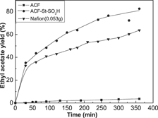
A sulfonated activated carbon fiber catalyst (SACF) was prepared through γ-irradiation-induced grafting of styrene onto the surface of activated carbon fiber (ACF) with an irradiation dose of 0.837 kGy/h for 48 h that was then sulfonated with chlorosulfonic acid under mild reaction conditions. Scanning electron microscopy observation showed that the ACF was wrapped by a thin layer of copolymer, and Fourier transfer infrared spectroscopy analysis indicated that sulfonic acid groups were successfully introduced onto the ACF. Pore structure analysis based on nitrogen adsorption isotherms at 77 K demonstrated that pore parameters of ACF were well maintained after the process of grafting and sulfonation modification. Proper conditions for the SACF preparation were sulfonated at 80 °C for 1.5 h in the 20% mass percentage of chlorosulfonic acid solution using ACF precursor, whose acid density could reach 1.47 mmol/g. The sulfonated ACF was used as catalyst for the esterification of acetic acid and ethanol. Evaluation of the catalytic activity of SACF showed evident advantages over other typical catalyst, with a turnover frequency value of 0.780 min−1, about five times higher than Nafion.
Carbon microspheres (CMSs) were oxidized by a mixture of concentrated sulfuric acid and nitric acid (ratio of 3:1 by volume) to improve their surface activity. Then, poly(3-hexylthiophene):CMSs (P3HT:CMSs) composite film was prepared by spin-coating method with oxidized CMSs and P3HT mixture chloroform solution. Energy levels of oxidized CMSs were investigated by cyclic voltammetry, the morphology of the composite films was characterized by atomic force microscopy, optical performance was analyzed by ultraviolet–visible spectrophotometry and fluorescent spectrometry, and microstructures of the products were characterized by Fourier transformation infrared spectrometry and x-ray diffraction. The results indicate that suspension concentration of 30 mg/mL and spinning rate of 2500 rpm were appropriate for fabricating P3HT:CMSs composite films. Optical properties of the P3HT:CMSs blends were changed by annealing. This lays an experimental foundation for fabricating active layer of polymer solar cells with high photoelectric conversion and low cost.
A Zn2SnO4/graphene (Zn2SnO4/G) hybrid was prepared by a facile one-pot hydrothermal route using SnCl4·5H2O, ZnSO4·7H2O, and graphite oxide as the precursors and NaOH as the mineralizer. Microsized Zn2SnO4 crystals with an octahedral shape are firmly confined by the graphene sheets, forming a unique hybrid structure. The confining effect of graphene leads to a more homogeneous size distribution of Zn2SnO4 crystals in Zn2SnO4/G than in bare Zn2SnO4. The introduction of graphene also brings an improved Li-storage performance for Zn2SnO4 due to the combined buffering, conducting, and confining effects of graphene. After being cycled at 200 mA/g for 50 times, Zn2SnO4/G can still keep a charge capacity of 326 mAh/g, while for bare Zn2SnO4, its charge capacity drops to only 100 mAh/g after the same cycles.