Refine search
Actions for selected content:
106100 results in Materials Science
What is the future for nuclear power?
-
- Journal:
- MRS Bulletin / Volume 36 / Issue 6 / June 2011
- Published online by Cambridge University Press:
- 10 June 2011, p. 415
- Print publication:
- June 2011
-
- Article
-
- You have access
- HTML
- Export citation
MRS volume 36 issue 6 Cover and Back matter
-
- Journal:
- MRS Bulletin / Volume 36 / Issue 6 / June 2011
- Published online by Cambridge University Press:
- 10 June 2011, pp. b1-b2
- Print publication:
- June 2011
-
- Article
-
- You have access
- Export citation
France’s nuclear power program continues in force
-
- Journal:
- MRS Bulletin / Volume 36 / Issue 6 / June 2011
- Published online by Cambridge University Press:
- 10 June 2011, pp. 418-421
- Print publication:
- June 2011
-
- Article
-
- You have access
- HTML
- Export citation
CAREER CENTRAL
-
- Journal:
- MRS Bulletin / Volume 36 / Issue 6 / June 2011
- Published online by Cambridge University Press:
- 10 June 2011, pp. 469-471
- Print publication:
- June 2011
-
- Article
-
- You have access
- Export citation

Photon management for photovoltaics
-
- Journal:
- MRS Bulletin / Volume 36 / Issue 6 / June 2011
- Published online by Cambridge University Press:
- 10 June 2011, pp. 424-428
- Print publication:
- June 2011
-
- Article
-
- You have access
- HTML
- Export citation
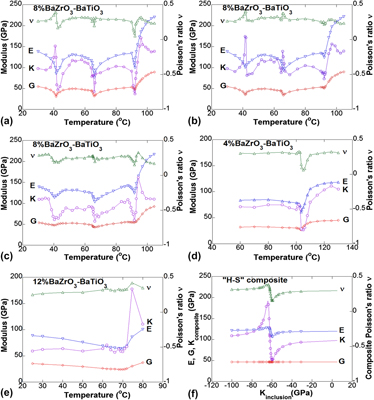
Viscoelastic sigmoid anomalies in BaZrO3–BaTiO3 near phase transformations due to negative stiffness heterogeneity
-
- Journal:
- Journal of Materials Research / Volume 26 / Issue 11 / 14 June 2011
- Published online by Cambridge University Press:
- 01 June 2011, pp. 1446-1452
- Print publication:
- 14 June 2011
-
- Article
- Export citation

Coherent light trapping in thin-film photovoltaics
-
- Journal:
- MRS Bulletin / Volume 36 / Issue 6 / June 2011
- Published online by Cambridge University Press:
- 10 June 2011, pp. 453-460
- Print publication:
- June 2011
-
- Article
- Export citation
Dielectric and electric field–induced pyroelectric behavior of (Pb0.87−0.07xBa0.10+0.07x)La0.02(Zr0.7Sn0.15Ti0.15)O3 ceramics
-
- Journal:
- Journal of Materials Research / Volume 26 / Issue 11 / 14 June 2011
- Published online by Cambridge University Press:
- 01 June 2011, pp. 1436-1440
- Print publication:
- 14 June 2011
-
- Article
- Export citation

Self-separated PZT thick films with bulk-like piezoelectric and electromechanical properties
-
- Journal:
- Journal of Materials Research / Volume 26 / Issue 11 / 14 June 2011
- Published online by Cambridge University Press:
- 01 June 2011, pp. 1431-1435
- Print publication:
- 14 June 2011
-
- Article
- Export citation

Plasmonics and nanophotonics for photovoltaics
-
- Journal:
- MRS Bulletin / Volume 36 / Issue 6 / June 2011
- Published online by Cambridge University Press:
- 10 June 2011, pp. 461-467
- Print publication:
- June 2011
-
- Article
- Export citation

High-performance antireflection coatings utilizing nanoporous layers
-
- Journal:
- MRS Bulletin / Volume 36 / Issue 6 / June 2011
- Published online by Cambridge University Press:
- 10 June 2011, pp. 434-438
- Print publication:
- June 2011
-
- Article
- Export citation
Nano Focus: Click coupling conjugated polymers to semiconductor nanorods
-
- Journal:
- MRS Bulletin / Volume 36 / Issue 6 / June 2011
- Published online by Cambridge University Press:
- 10 June 2011, p. 405
- Print publication:
- June 2011
-
- Article
-
- You have access
- HTML
- Export citation
Study helps explain superconducting behavior of metallic, insulating pnictides
-
- Journal:
- MRS Bulletin / Volume 36 / Issue 6 / June 2011
- Published online by Cambridge University Press:
- 10 June 2011, pp. 405-406
- Print publication:
- June 2011
-
- Article
-
- You have access
- HTML
- Export citation
LOOK AGAIN…
-
- Journal:
- MRS Bulletin / Volume 36 / Issue 6 / June 2011
- Published online by Cambridge University Press:
- 10 June 2011, p. 472
- Print publication:
- June 2011
-
- Article
-
- You have access
- HTML
- Export citation
Energy Focus
-
- Journal:
- MRS Bulletin / Volume 36 / Issue 6 / June 2011
- Published online by Cambridge University Press:
- 10 June 2011, p. 422
- Print publication:
- June 2011
-
- Article
-
- You have access
- HTML
- Export citation
Microstructural and electrical properties of Ce0.9Gd0.1O1.95 thin film electrolyte in solid oxide fuel cells – CORRIGENDUM
-
- Journal:
- Journal of Materials Research / Volume 26 / Issue 11 / 14 June 2011
- Published online by Cambridge University Press:
- 01 June 2011, E1
- Print publication:
- 14 June 2011
-
- Article
- Export citation
Nano Focus: Nanofiltration membrane improves performance of vanadium redox flow battery
-
- Journal:
- MRS Bulletin / Volume 36 / Issue 6 / June 2011
- Published online by Cambridge University Press:
- 10 June 2011, pp. 410-411
- Print publication:
- June 2011
-
- Article
-
- You have access
- HTML
- Export citation
Bio Focus: Liquid STEM used for particle uptake studies in living cells
-
- Journal:
- MRS Bulletin / Volume 36 / Issue 6 / June 2011
- Published online by Cambridge University Press:
- 10 June 2011, p. 410
- Print publication:
- June 2011
-
- Article
-
- You have access
- HTML
- Export citation
Learning from failures
-
- Journal:
- MRS Bulletin / Volume 36 / Issue 6 / June 2011
- Published online by Cambridge University Press:
- 10 June 2011, pp. 416-417
- Print publication:
- June 2011
-
- Article
-
- You have access
- HTML
- Export citation
Energy Focus: Conjugated microporous polymer networks chemically tuned for CO2 adsorption
-
- Journal:
- MRS Bulletin / Volume 36 / Issue 6 / June 2011
- Published online by Cambridge University Press:
- 10 June 2011, pp. 408-410
- Print publication:
- June 2011
-
- Article
-
- You have access
- HTML
- Export citation
