To save content items to your account,
please confirm that you agree to abide by our usage policies.
If this is the first time you use this feature, you will be asked to authorise Cambridge Core to connect with your account.
Find out more about saving content to .
To save content items to your Kindle, first ensure no-reply@cambridge.org
is added to your Approved Personal Document E-mail List under your Personal Document Settings
on the Manage Your Content and Devices page of your Amazon account. Then enter the ‘name’ part
of your Kindle email address below.
Find out more about saving to your Kindle.
Note you can select to save to either the @free.kindle.com or @kindle.com variations.
‘@free.kindle.com’ emails are free but can only be saved to your device when it is connected to wi-fi.
‘@kindle.com’ emails can be delivered even when you are not connected to wi-fi, but note that service fees apply.
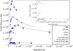
Experimental and simulation studies have shown that decreasing the grain size below a critical value results in softening rather than hardening in both the yield stress and flow stress of nanomaterials. In this work, a gradient plasticity framework is presented that can capture this softening behavior by treating grain boundaries as a separate phase with a finite thickness. The theoretical expression obtained for the yield stress as a function of the grain size can capture numerous experimental data that exhibit this “normal” to “abnormal” Hall–Petch transition, and an analytical equation is obtained that can predict the grain size at which this transition occurs. Furthermore, analytical expressions are obtained for the flow stress in nanomaterials, and they are in precise agreement with atomistic simulations on nanocrystalline Cu, which predict that below a critical grain size the flow stress decreases proportional to it.
Elastic modulus and internal friction of Ba0.5Sr0.5Co0.8Fe0.2O3-δ (BSCF) and La0.58Sr0.4Co0.2Fe0.8O3-δ (LSCF) were determined from resonance frequencies and damping behavior, respectively, using an impulse excitation method. An elastic anomaly for BSCF around 476 K, with a corresponding peak in the internal friction, is attributed to the experimentally confirmed spin transition of Co3+. LSCF is in a ferromagnetic state below ∼220 K and in a paramagnetic state above ∼250 K. The elastic modulus of LSCF exhibits an anomaly between 473 and 1113 K, which is attributed to a transition from rhombohedral to cubic symmetry.
This study describes the elimination of threading dislocations (TDs) in GaN nanostructures. Cross-sectional transmission electron microscopy (XTEM) analysis reveals that the nominal [0001] line direction of a TD changes when it enters a GaN nanostructure and the dislocation then terminates at a sidewall facet. It is suggested that the driving force for this process is the reduction of dislocation line energy, and for a pure-edge dislocation, this TD elimination process can be accomplished simply by dislocation climb. This mechanism is active whenever a threading defect is in close proximity to a surface. Preliminary XTEM analysis of defects in AlGaN and InGaN core–shell growth onto GaN nanostructures is also shown. Although more work is required to improve the quality of core–shell InGaN epitaxial growth, nanostructures appear to offer a route to defect-free, nonpolar GaN-based devices.
Urchin-like γ-MnO2 nanostructures, composed of nanowires with diameters in the range 40–70 nm were prepared through the direct reaction between MnSO4 and KClO3 via a mild hydrothermal route. Reaction time and temperature were found to influence both the phase and morphology of as-prepared products. For longer reaction times, the initially formed γ-phase transformed to α-MnO2 nanowires along with the loss of urchin-like morphology. Powder x-ray diffraction (XRD), scanning electron microscopy (SEM), energy dispersive x-ray spectroscopy, Fourier transform infrared spectroscopy, and thermogravimetry and differential scanning calorimetry were used to characterize the as-prepared products. On the basis of XRD patterns and SEM images, a possible growth mechanism for the time-dependant morphological evolution of various MnO2 nanostructures has been suggested and discussed.
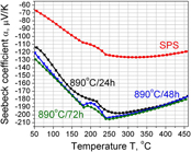
Si80Ge20B0.6 thermoelectric alloys with minute erbium (Er) addition were prepared by the spark plasma sintering technique. The samples with different amounts of Er additions were analyzed by x-ray diffraction, x-ray fluorescence, and x-ray photoelectron spectroscopy. The thermoelectric properties were measured from 400 to 900 K. Effects of the amount of Er addition on the thermoelectric properties of Si80Ge20B0.6 alloys were investigated. New findings indicate that the Er-added alloys have larger carrier concentrations than the pristine sample. The larger carrier concentration appears to make a significant contribution to the electrical conductivity. Seebeck coefficient decreases with the increase of carrier concentration, whereas the power factor increases with increasing electrical conductivity. It was generally believed that the scattering of phonons by carriers may result in the thermal conductivity reduction. The samples with Er addition exhibit better figure of merits than the pristine sample. The optimal ratio of Er addition is actually in the range of 0.085–0.125 at.%.
Metallic nanostructures and specifically nanowires can be used for technological breakthroughs. Experimental measurements have provided insights on the mechanical properties of metallic nanostructures. In conjunction, modeling analyses provide an understanding of the underlying deformation and strengthening mechanisms in nanostructures. Most modeling studies on nanostructures are based on atomistic and molecular dynamics simulations, and though invaluable, they are limited to nanoscale dimensions of a few tens of nanometers, at small temporal scales, and physically unrealistic strain rates. Furthermore, most of the current applications for free-standing metallic nanostructures require high aspect ratios with at least one dimension greater than a few hundred nanometers. A continuum microstructurally based approach can, therefore, provide insights on design of one-dimensional nanowires on a physically relevant scale. Hence, we use a multiple-slip crystal plasticity formulation that is adapted to single crystal gold nanowires to simulate the experimental setup for a two-end fixed nanowire subjected to bending.
Half-Heusler (HH) and especially TiNiSn-based alloys have shown high potential as thermoelectric (TE) materials for power generation applications. The reported transport properties show, however, a significant spread of results, due mainly to the difficulty in fabricating single-phase HH samples in these multicomponent and multiphased systems. In particular, little attention has been paid to the influence of the various minority phases on the TE performance of these compounds. A clear understanding of these issues is mandatory for the design of improved and stable TE HH-based composites. This study examines the structural and compositional influence of the residual metallic (Sn) and intermetallic phases (mainly Ti6Sn5 and the Heusler compound TiNi2Sn) on the TE properties of the TiNiSn HH compounds processed by spark plasma sintering.
The Si–P system at high temperatures up to 6 wt%P was investigated. Silicon–phosphorus alloys were prepared through the melting of silicon–phosphorus mixtures in closed silica tubes. Microstructural studies indicated two phases in the alloys, i.e., a solid solution of P in Si and the intermediate compound SiP. Thermal analysis technique was applied to study the phase transformations in the alloys at elevated temperatures. It was observed that SiP is melted at 1139 ± 2 °C. A eutectic reaction in the system, in which liquid Si–P alloy is transformed to SiP and a solid solution of P in Si was observed at 1129 ± 2 °C. Moreover, the liquidus and solidus on the silicon-rich part of the phase diagram were determined as:
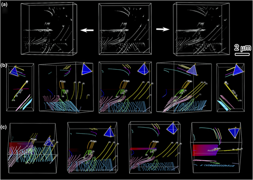
The material characterization toolbox has recently experienced a number of parallel revolutionary advances, foreshadowing a time in the near future when material scientists can quantify material structure evolution across spatial and temporal space simultaneously. This will provide insight to reaction dynamics in four-dimensions, spanning multiple orders of magnitude in both temporal and spatial space. This study presents the authors’ viewpoint on the material characterization field, reviewing its recent past, evaluating its present capabilities, and proposing directions for its future development. Electron microscopy; atom probe tomography; x-ray, neutron and electron tomography; serial sectioning tomography; and diffraction-based analysis methods are reviewed, and opportunities for their future development are highlighted. Advances in surface probe microscopy have been reviewed recently and, therefore, are not included [D.A. Bonnell et al.: Rev. Modern Phys. in Review]. In this study particular attention is paid to studies that have pioneered the synergetic use of multiple techniques to provide complementary views of a single structure or process; several of these studies represent the state-of-the-art in characterization and suggest a trajectory for the continued development of the field. Based on this review, a set of grand challenges for characterization science is identified, including suggestions for instrumentation advances, scientific problems in microstructure analysis, and complex structure evolution problems involving material damage. The future of microstructural characterization is proposed to be one not only where individual techniques are pushed to their limits, but where the community devises strategies of technique synergy to address complex multiscale problems in materials science and engineering.
SiGe alloys belong to the class of classic high temperature thermoelectric materials. By the means of nanostructuring, the performance of this well-known material can be further enhanced. Additional grain boundaries and point defects added to the alloy structure result in a strong decrease in thermal conductivity because of reduced lattice contribution to the overall thermal conductivity. Hence, the figure of merit can be increased. To obtain a nanostructured bulk material, a nanosized raw material is essential. In this work, a new approach toward nanostructured SiGe alloys is presented where alloyed nanoparticles are synthesized from a homogeneous mixture of the respective precursors in a microwave plasma reactor. As-prepared nanoparticles are compacted to a dense bulk material by a field assisted sintering technique. A figure of merit of zT = 0.5 ± 0.09 at 450 °C and a peak zT of 0.8 ± 0.15 at 1000 °C could be achieved for a nanostructured, 0.8% phosphorus-doped Si80Ge20 alloy without any further optimization.
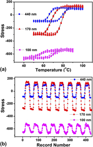
We report on in situ stress relaxation behavior of vanadium dioxide thin films across the thermally driven metal–insulator transition (MIT) and size effects. Although the residual stress follows an inverse relationship with film thickness, the metal–insulator phase transition-induced stress varies nonmonotonically with increase in film thickness and grain size. Maximum transformation stress of −447 MPa is observed across the MIT for ∼170-nm-thick film with an average grain size of ∼70 nm. The interplay between constraint effects and nanostructure leads to nontrivial stress relaxation trends and provides insights into design of phase transition materials for switching devices.
We report a novel approach to realize the formation of well-distributed nanodispersions in n-type filled skutterudite through the manipulation of metastable void fillers by a designed sophisticated process of materials synthesis. Metastable Ga filling in CoSb3 is proved to happen at high temperature. The subsequent controlled annealing procedure drives Ga out of the crystal voids and finally leads to the homogeneous dispersion of GaSb nanodots with an average size of 11 nm in CoSb3 matrix. The grain size of nanodispersions can be manipulated by the controlled cooling procedure. The well-distributed nanodispersions are observed to enhance Seebeck coefficients and reduce lattice thermal conductivity at low temperature. Therefore, the thermoelectric performance of nanocomposite is improved in the whole temperature range. The highest figure of merit (ZT) is obtained to be 1.45 at 850 K, and an average ZT of 0.99 in 300−850 K is achieved for Yb0.26Co4Sb12/0.2GaSb nanocomposite.
A one-step wet chemistry route has been explored to synthesize hollow hydroxyl titanium oxalate nanoscale spheres under mild experimental conditions. The hollow spheres were ∼200 nm in diameter, with a shell thickness of ∼30 nm. The nanospheres were formed by smaller aggregated colloidal subunits. The influence of temperature and solvent on the structure of the nanospheres was investigated. The formation of hollow interiors in the nanospheres may be rationalized by Ostwald ripening mechanism. Simple thermal treatment topotactically transformed the chemical composition into anatase TiO2. The high-order hollow porous spherical structure was preserved, with smaller crystalline anatase TiO2 nanoparticles as building units. Dense hydroxyl titanium oxalate nanospheres and their corresponding non-hollow porous anatase TiO2 nanospheres were also successfully achieved in suitable reaction conditions. The method and procedure reported herein may be extended in principle for the fabrication of other functional materials.
Nowotny chimney-ladder compounds RuAl2 and RuGa2 have been substituted with p- and n-type dopants to study the resistivity, Seebeck and Hall coefficients, and thermal conductivity of resulting compounds in the temperature range of 80–300 K. The resistivity and Seebeck coefficient suggest that these compounds are degenerate semiconductors. Hall measurements reveal that the carrier concentration has indeed been changed by an order of magnitude, particularly in p-type RuGa2 by substituting Cr and Mn. Compared to p-type samples, the resistivity is an order of magnitude larger for n-type samples, for a similar level of carrier concentration. Interestingly, the hole mobility is two to three orders of magnitude larger, reaching the highest value of ∼750 cm2/V·s. The electron mobility is temperature independent and is typically in the range of ∼1–4 cm2/V·s. Thermal conductivity shows characteristics of mixed scattering with impurity scattering contributing appreciably in heavily substituted compositions.
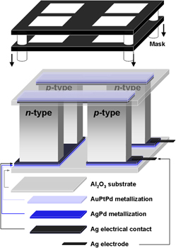
Four-leg thermoelectric oxide modules (TOMs) consisting of two p-type (La1.98Sr0.02CuO4) and two n-type (CaMn0.98Nb0.02O3) thermoelectric (TE) legs were produced with a manufacturing quality factor between 30 and 60%. The pressed sintered TE legs revealed 90% of the theoretical density to ensure a sufficient mechanical stability of the TE modules. The legs were connected electrically in series and sandwiched thermally in parallel between two Al2O3 plates serving as absorber and cooler, respectively. A solar cavity-receiver packed with an array of TOMs was subjected to concentrated thermal radiation with peak solar radiative flux intensities exceeding 600 kW/m2. Temperature distributions in the cavity, open-circuit voltage (VOC), and maximum output power (Pmax) were measured for different external loads and solar radiative fluxes (qin). Finally, the solar-to-electricity conversion efficiency (η) was calculated.
Indium has attracted much attention as a beneficial addition to cobalt–antimony-based skutterudites as a result of good thermoelectric performance. In this study, as-cast InxCo4Sb12 with x = 0.05, 0.2 were examined using x-ray diffraction analysis and scanning electron microscopy. For x = 0.2 we found, besides the skutterudite main phase, nanometer-sized regions of secondary phases distributed along the grain boundaries, which exhibit substructures. As-cast material with x = 0.05 does not show visible precipitates. We further observed that changing one of the heat treatment parameters of In0.2Co4Sb12 has a major effect on the microstructure and shape of the precipitates, but minor influence on the skutterudite matrix composition. Energy dispersive x-ray spectroscopy analysis by transmission electron microscopy) reveals that indium is to a large extent distributed into the skutterudite structure. Measurements of short-term sintered material confirm that the addition of indium and particularly the modification of the synthesis parameter entails to an enhanced ZT.
A nanoindentation strain-rate jump technique has been developed for determining the local strain-rate sensitivity (SRS) of nanocrystalline and ultrafine-grained (UFG) materials. The results of the new method are compared to conventional constant strain-rate nanoindentation experiments, macroscopic compression tests, and finite element modeling (FEM) simulations. The FEM simulations showed that nanoindentation tests should yield a similar SRS as uniaxial testing and generally a good agreement is found between nanoindentation strain-rate jump experiments and compression tests. However, a higher SRS is found in constant indentation strain-rate tests, which could be caused by the long indentation times required for tests at low indentation strain rates. The nanoindentation strain-rate jump technique thus offers the possibility to use single indentations for determining the SRS at low strain rates with strongly reduced testing times. For UFG-Al, extremely fine-grained regions around a bond layer exhibit a substantial higher SRS than bulk material.
The Maugis–Barquins (MB) solutions for the adhesive contact between an axisymmetric indenter and an elastic half-space are modified by incorporating the interfacial energy defined by the real area of contact. With the modified MB solutions, general relations for contact stiffness including adhesive effects in indentation analysis are derived. Numerical calculations showed that the difference in expected stiffness for the modified MB model compared to the standard MB results can be significant at low loads of interest in atomic force microscopy measurements and also for indentation tests at high load if the interfacial energy is large (∼0.1 J/m2) and the material is soft (Young’s modulus ≤100 MPa).
Optical metamaterials are an exciting new field in optical science. A rapidly developing class of these metamaterials are those that allow the manipulation of volume and surface electromagnetic waves in desirable ways by suitably structuring the surfaces they interact with. They have applications in a variety of fields, such as materials science, photovoltaic technology, imaging and lensing, beam shaping and lasing. Describing techniques and applications, this book is ideal for researchers and professionals working in metamaterials and plasmonics, as well as those just entering this exciting new field. It surveys different types of structured surfaces, their design and fabrication, their unusual optical properties, recent experimental observations and their applications. Each chapter is written by an expert in that area, giving the reader an up-to-date overview of the subject. Both the experimental and theoretical aspects of each topic are presented.