To save content items to your account,
please confirm that you agree to abide by our usage policies.
If this is the first time you use this feature, you will be asked to authorise Cambridge Core to connect with your account.
Find out more about saving content to .
To save content items to your Kindle, first ensure no-reply@cambridge.org
is added to your Approved Personal Document E-mail List under your Personal Document Settings
on the Manage Your Content and Devices page of your Amazon account. Then enter the ‘name’ part
of your Kindle email address below.
Find out more about saving to your Kindle.
Note you can select to save to either the @free.kindle.com or @kindle.com variations.
‘@free.kindle.com’ emails are free but can only be saved to your device when it is connected to wi-fi.
‘@kindle.com’ emails can be delivered even when you are not connected to wi-fi, but note that service fees apply.
Despite extensive research, the understanding of the fundamental processes governing yielding and plastic flow in metallic glasses remains poor. This is due to experimental difficulties in capturing plastic flow as a result of a strong localization in space and time by the formation of shear bands at low homologous temperatures. Unveiling the mechanism of shear banding is hence key to developing a deeper understanding of plastic deformation in metallic glasses. We will compile recent progress in studying the dynamics of shear-band propagation from serrated flow curves. We will also take a perspective gleaned from stick-slip theory and show how the insights gained can be deployed to explain fundamental questions concerning the origin, mechanism, and characteristics of flow localization in metallic glasses.
We demonstrate Er3+ diffusivity and solubility increases in off-congruent, Li-deficient LiNbO3 crystal. Li-poor vapor transport equilibration was used to reduce Li2O content in initial congruent crystals. Local Er3+ in-diffusion was then performed in a wet O2 atmosphere. Before and after the Er3+ diffusion procedure, surface Li2O content was evaluated from measured birefringence. The results show that the Er3+ diffusion procedure resulted in 0.3–0.5 mol% Li2O content loss at crystal surface. Secondary ion mass spectrometry was used to measure the Er3+ depth profiles, from which the diffusivity and solubility are determined. It is shown that the Er3+ diffusivity is nearly doubled and the solubility increases at least 0.6 mol% as the Li2O content decreases by 1.0 mol%. From the known Li2O content reduction, the solubility increase is also predicted and the results show that the predicted data are considerably smaller than the experimental results, suggesting that the Er3+ ions occupy also the Nb5+ site, besides the Li+ site.
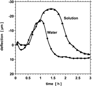
Breakdown of porous materials by salts occurs when growing crystals exert pressure on the pore walls, inducing stress in the material that exceeds its tensile strength. In this work, we quantify the mechanical stresses caused by a particularly destructive mechanism: the dissolution of an anhydrate (thenardite, Na2SO4) followed by precipitation of a hydrated salt (mirabilite, Na2SO4·10H2O). Stresses are measured using a composite specimen consisting of a plate of glass bonded to a plate of limestone (CaCO3) whose pores are impregnated with thenardite. As water wicks into the limestone, thenardite dissolves and mirabilite precipitates. The limestone expands from the pressure exerted by the salt resulting in deflection of the composite, and the stresses can be obtained from an elastic analysis. Synchrotron x-ray diffraction reveals the dissolution–crystallization rate. Numerical modeling shows that the stresses are affected by the kinetics of crystallization and dissolution, permeability, and mechanical properties of the stone, allowing us to determine the amount of salt that causes material fracture.
The time-resolved evolution of intermetallic phase formation in the system pure Sn (polycrystalline coating with a thickness of several microns) on pure Cu (polycrystalline bulk substrate) was investigated in detail by means of focused ion beam and transmission electron microscopy and x-ray diffraction during aging at room temperature for a period of about 1 year. The availability of this coherent data base allowed interpretation of the evolution of intermetallic compound (IMC) formation in terms of interface thermodynamics and interdiffusion kinetics. On this basis spontaneous Sn whiskering on the surface of the Sn coating as a consequence of intermetallic phase (Cu6Sn5) formation along, specifically, Sn grain boundaries intersecting the Sn/Cu interfaces could be discussed. Moreover, a treatment to mitigate spontaneous Sn whiskering on the basis of thermodynamic control of the IMC morphology was proposed.
Second nearest-neighbor modified embedded-atom method (MEAM) interatomic potentials for the Al–H and Ni–H binary systems have been developed on the basis of previously developed MEAM potentials of pure Al, Ni, and H. The potentials can describe various fundamental physical properties of the relevant binary alloys (structural, thermodynamic, defect, and dynamic properties of metastable hydrides or hydrogen in face-centered cubic solid solutions) in good agreement with experiments or first-principles calculations. The applicability of the present potentials to atomic level investigations of dynamic behavior of hydrogen atoms in metal membranes is also discussed.
The formation of interfacial η′-Cu6Sn5 in Sn–0.7Cu/Cu solder joints at different aging temperatures was studied using x-ray diffraction (XRD). The time-temperature-formation curve was obtained and is discussed based on the phase transformation from existing η-Cu6Sn5 and interfacial reaction at temperatures below 186 °C. A minimum formation time was observed in the temperature range of 135–150 °C.
A novel and previously unreported, high temperature solid–liquid–solid (SLS) silica nanowire (NW) growth mode has been observed and investigated. In this mode, SLS NW nucleation and subsequent growth was uniquely promoted by—and coupled to—the formation of thermally etched pyramidal pits in the Si substrate that formed during a high temperature anneal phase before the onset of SLS NW formation. The silicon oxide-mediated thermal pit formation process enhanced Si transport to Au–Si alloy droplets directly adjacent to the pyramidal pits. Consequently, SLS NW nucleation and growth was preferentially promoted at the pit edges. The promotion of SLS NW growth by the pyramidal pits resulted in the observation of SLS NW “blooms” at the pit locations. Subsequent NW growth, occurring both at the pit sites and from Au–Si alloy droplets distributed across the planar surfaces of the Si wafer, eventually occluded the pits. This newly observed process is termed as “thermal pit-assisted growth.”
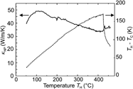
Arrays of vertically aligned silicon wires of 250 nm–4 μm in diameter were fabricated in a top–down process using photolithography and deep reactive ion etching at cryogenic temperatures. Using the 3-omega method, thermal conductance of vertical silicon nanowires, i.e., nanopillars, was measured immediately on-chip without the need of breaking off single wires and mounting them into a special testing device. The Seebeck coefficient was measured with 2-mm2 arrays of pillars of 260 nm in diameter, which were pressure-joined with bulk chips for testing. Testing was performed in the temperature range between 50 and 470 °C at applied temperature gradients of up to 190 °C. We found a reduction of the thermal conductivity to less than 30% of the bulk silicon, confirming that arrayed vertical nanowires fabricated in an economical top–down process can strongly promote silicon as a thermoelectric material.
We report the low-temperature synthesis and characterization of polyvinylpyrrolidone (PVP)-capped FeAu magneto-plasmonic multifunctional nanoparticles by a one-step nanoemulsion process. The Fourier transform infrared spectroscopy study proves the PVP coating on the surface of the resultant FeAu nanoparticles, whereas the structural, magnetic, and optical analysis illustrates the fusion of iron and gold into one single nanostructure showing the nanoparticle shape and a tight size distribution with an average size of 11.3 nm, followed by the growth habit compared to other relevant nanoparticles. Moreover, the PVP-capped FeAu nanoparticles manifest soft ferromagnetic behavior with a small coercivity of ∼40 Oe at room temperature. The corresponding magnetic hysteresis curves were elucidated by modified bi-phase Langevin equations, which were reasonably interpreted with the binary particle size distribution. The nanoparticles reveal a well-defined surface plasmon resonance band at ∼546 nm and a visual demonstration shows the magnetic separability of all nanoparticles for potential magnetic and/or optical manipulation.
It was observed that silicon and germanium nanowires can exhibit significant electrostatic charging and respond strongly to externally applied electric fields. This includes nanowires in air and dispersed in low-conductivity, low-dielectric-constant solvents such as hexane, toluene, and benzene. The electrostatic charging of semiconductor nanowires was investigated as a tool for nanowire manipulation. By charging a substrate, nanowires could be deposited on surfaces with very high coverage and onto selected locations of the surface. The density of deposited nanowires could be adjusted systematically by varying the strength of the electric field. Alternating electric fields, applied between two electrodes, resulted in nanowires oriented with respect to the field orientation.
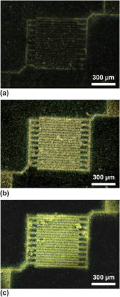
In this work, poly(2-ethyl-2-oxazoline) (PEtOx) is used for synthesis of silver-nanoparticle-embedded polymer nanofibers through a simple polyol process. The factors, such as AgNO3/PEtOx molar ratio R, reaction temperature T, and reaction time t, which would influence the morphology of the nanofiber were studied extensively. Long linear PEtOx nanofibers with length more than 1 μm were obtained under the optimum conditions of R = 5, T = 150 °C, and t = 1 h. PEtOx and reaction temperature were found to be the key factors affecting the final morphology of nanofibers in this system. The physical and chemical properties of these silver-nanoparticle-embedded PEtOx nanofibers were characterized by transmission electron microscopy, high-resolution transmission electron microscopy, energy dispersive spectrum, x-ray diffraction, and inductive coupled plasma-mass spectrometry. The growth mechanism of the nanofibers is elucidated, and the process is demonstrated to be both kinetically and thermodynamically controlled.
High-quality Zn3P2 nanowires are synthesized at a temperature as low as 350 °C using Zn foil and trioctylphosphine by chemical reflux method. Scanning electron microscopy and transmission electron microscopy (TEM) images show their diameters vary from ∼15 to 70 nm. Energy dispersive x-ray spectroscopy and nanobeam electron diffraction patterns in combination with structure factor simulation reveal that the nanowires have tetragonal α-Zn3P2 structure. Based on high-resolution TEM images and their fast Fourier transform patterns, Zn3P2 nanowires are considered to grow on a vicinity of the possibly highest surface energy plane of (101) with a growth direction parallel to [101].
We have successfully achieved a transconductance of 0.76 S/m for organic thin-film transistors with 4 V operation, which is the largest value reported for organic transistors fabricated using printing methods. Using a subfemtoliter inkjet, silver electrodes with a line width of 1 µm and a channel length of 1 µm were printed directly onto an air-stable, high-mobility organic semiconductor that was deposited on a single-molecule self-assembled monolayer-based gate dielectric. On reducing the droplet volume (0.5 fl) ejected from the inkjet nozzle, which reduces sintering temperatures down to 90 °C, the inkjet printing of silver electrodes was accomplished without damage to the organic semiconductor.
The growth kinetics of Si bulk crystals and nanowires (NWs) in contact with Au–Si liquids is studied by molecular dynamics simulations using an empirical potential fitted to the Au–Si binary phase diagram. The growth speed v is predicted as a function of Si concentration xSi in the Au–Si liquid at temperature T = 1100 K and as a function of T at xSi = 75%. For both bulk crystals and NWs, the {111} surface grows by the nucleation and expansion of a single two-dimensional island at small supersaturations, whereas the {110} surface grows simultaneously at multiple sites. The top surfaces of the NWs are found to be curved near the edges. The difference in the growth velocity between NWs and bulk crystals can be explained by the shift of the liquidus curve for NWs. For both bulk crystals and NWs, the growth speed diminishes in the low temperature limit because of reduced diffusivity.
Ruthenium dioxide (RuO2) was uniformly modified on TiO2 porous thin film by impregnation of Ru-contained dye on the film followed by sintering it at 450 °C to burn off organic matters and form ruthenium oxide, which is named as impregnation method. The homogenous modification of metal oxide inside porous thin film can be realized by the impregnation method, and the modification amount of RuO2 can be easily adjusted by the iteration numbers of impregnation and sintering. Appropriate amount of uniformly modified RuO2 was found to obviously enhance photocatalytic performance of TiO2 to degrade eosin Y. The photocatalysis enhancement was attributed to the shallow hole traps on the surface of nanoparticles formed by RuO2, and these traps can retard recombination of hole with electron.
We investigate the collective effect of a high volume fraction of ∑3 twin boundaries on the response of nanotwinned Cu to high dose He implantation near room temperature and find that they do not curtail the formation of vacancy and interstitial clusters. This result is rationalized through atomistic modeling, which shows that point defects at these boundaries have nearly identical properties to those in pure fcc Cu.