To save content items to your account,
please confirm that you agree to abide by our usage policies.
If this is the first time you use this feature, you will be asked to authorise Cambridge Core to connect with your account.
Find out more about saving content to .
To save content items to your Kindle, first ensure no-reply@cambridge.org
is added to your Approved Personal Document E-mail List under your Personal Document Settings
on the Manage Your Content and Devices page of your Amazon account. Then enter the ‘name’ part
of your Kindle email address below.
Find out more about saving to your Kindle.
Note you can select to save to either the @free.kindle.com or @kindle.com variations.
‘@free.kindle.com’ emails are free but can only be saved to your device when it is connected to wi-fi.
‘@kindle.com’ emails can be delivered even when you are not connected to wi-fi, but note that service fees apply.
A systematic investigation of the intermetallic phase Ru1-yIn3 (0 ≤ y ≤ 0.025) and its substitution derivatives RuIn3-xSnx and RuIn3-xZnx (x = 0.01, 0.025, 0.05, and 0.1) is performed. The samples were prepared from a liquid–solid reaction of components with subsequent spark plasma sintering treatment. Ru1-yIn3 exhibits n- and p-type behavior crossing over from low to high temperatures. Substitution of indium by tin or zinc up to 2.5 at.% leads to an increase of the charge carrier concentration, with negative (Sn) or positive (Zn) Seebeck values, respectively. The electrical resistivity was P changed from semiconductor- to metal-like properties by substitution, whereas the thermal conductivity was reduced down to 50% of that of RuIn3. Higher values of the thermoelectric figure of merit were achieved by chemical substitution (RuIn3-xSnx, RuIn3-xZnx), opening up a possibility for tuning the thermoelectric properties in this class of materials.
Ferromagnetic resonance investigations on Ni nanowires are reported. The angular dependence of the resonance line position is analyzed within a thermodynamic approach that includes shape anisotropy (ellipsoids of revolution), magnetocrystalline anisotropies (cubic and uniaxial), and dipole–dipole interactions. The results are supported by hysteresis loops, obtained on the same sample.
We have synthesized single- and polycrystal Ba8AlxSi46−x clathrates to compare their thermoelectric properties. Single-crystal sample was prepared by Czochralski method in an argon atmosphere. Polycrystal sample was prepared by arc melting and annealed at 850 °C for 100 h in an argon atmosphere. The Seebeck coefficients of single- and polycrystal Ba8Al12Si34 at 500 °C were 44.5 and 53.0 μV/K, respectively. The Seebeck coefficients of both samples were almost the same because the Seebeck coefficients depend on carrier concentration, which is related to aluminum content. The electrical resistivity of the single-crystal sample with 0.49 mΩcm was lower than that of the polycrystal sample with 0.95 mΩcm because of the reduction of electron scattering. Therefore, the power factor of the single-crystal sample with 4.0 × 10⁻⁴ V2/K2Ωm was higher than that of the polycrystal sample with 3.0 × 10⁻⁴ V2/K2Ωm at 500 °C. It is suggested that single crystallization is efficient for improvement of the thermoelectric property in the Ba8AlxSi46−x clathrate.
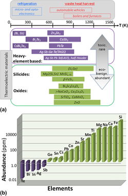
Most state-of-the-art thermoelectric (TE) materials contain heavy elements Bi, Pb, Sb, or Te and exhibit maximum figure of merit, ZT∼1–2. On the other hand, oxides were believed to make poor TEs because of the low carrier mobility and high lattice thermal conductivity. That is why the discoveries of good p-type TE properties in layered cobaltites NaxCoO2, Ca4Co3O9, and Bi2Sr2Co2O9, and promising n-type TE properties in CaMnO3- and SrTiO3-based perovskites and doped ZnO, broke new ground in thermoelectrics study. The past two decades have witnessed more than an order of magnitude enhancement in ZT of oxides. In this article, we briefly review the challenges, progress, and outlook of oxide TE materials in their different forms (bulk, epitaxial film, superlattice, and nanocomposites), with a greater focus on the nanostructuring approach and the late development of the oxide-based TE module.
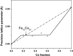
Amorphous ribbons of (Fe1-xCox)88Zr7B4Cu1 (x = 0.2, 0.35, 0.5, and 0.6) alloys were annealed to produce a nanocrystalline phase dispersed in the amorphous matrix. Precision lattice parameter calculation showed that composition of the nanocrystalline phase is Fe73Co27 for all the alloys irrespective of initial alloy composition. This result was well corroborated with the Mössbauer results. Saturation magnetization of annealed ribbons was almost same for all the alloys, however, coercivity increases with Co content.
Syntaxial growth of Mn11Ge8/Ge nanowire heterostructures was carried out using a vapor–solid–solid (VSS) growth process, and transmission electron microscopy imaging and selected-area electron diffraction were used to study the structure, orientation, and interface of each phase. Preferred crystallographic relationships were found to exist between the Mn11Ge8 seeds, which exhibit a single uniaxial growth direction, and the seeded Ge nanowires, which exhibit multiple growth directions. The crystallographic relationships for individual nanowire heterostructures were characterized in the context of microtexture analysis, which has not previously been applied to nanowire heterostructures. Fiber and off-normal fiber textures were predominant, although examples of epitaxial and uniaxial in-plane textures were also identified. Microtexture analysis of VSS-grown nanowire systems is shown to provide a useful perspective on the products of synthesis that can lead to new insights into growth mechanisms.
We have studied the effects of focused-ion-beam (FIB) irradiation and prestraining on the mechanical properties of nearly defect-free Au microparticles on a sapphire substrate. The Au microparticles, which were produced by a solid-state diffusion dewetting technique, were FIB-irradiated and/or prestrained, the latter using a nanoindenter with a flat ended punch operating under a nanohammering mode. Also, the prestrained Au microparticles were exposed to FIB to examine the effects of ion-beam damage on the properties of crystals containing mobile dislocations. We found that both FIB irradiation and prestraining reduced the yield strength of pristine Au microparticles significantly and made the stress–strain curves jerky. However, FIB irradiation does not affect the mechanical properties of prestrained Au microparticles very significantly. Once a microparticle contains mobile dislocations, its mechanical properties are not influenced much by the defects generated by FIB irradiation, even at the submicrometer scale.
We review the position-controlled growth of III-V nanowires (NWs) by selective-area metal-organic vapor-phase epitaxy (SA-MOVPE). This epitaxial technique enables the positioning of the vertical NWs on (111) oriented surfaces with lithographic techniques. Core-shell structures have also been achieved by controlling the growth mode during SA-MOVPE. The core-shell III-V NW-based devices such as light-emitting diodes, photovoltaic cells, and vertical surrounding-gate transistors are discussed in this article. Nanometer-scale growth also enabled the integration of III-V NWs on Si regardless of lattice mismatches. These demonstrated achievements should have broad applications in laser diodes, photodiodes, and high-electron mobility transistors with functionality on Si not made possible with conventional Si-CMOS techniques.
A dislocation-density grain–boundary (GB) interaction scheme for face-centered cubic bicrystals with three coincident site lattice boundaries was developed to account for the interrelated dislocation-density interactions of GB emission, absorption, and transmission. The proposed GB scheme was coupled to a dislocation-density multiple-slip crystalline plasticity formulation and specialized finite-element algorithms to account for behavior on the microstructural scale. A conservation law for dislocation densities was also used to balance dislocation-density absorption, transmission, and emission within the GB region. The predictions indicated that GB absorption increases are due to increases in immobile dislocation densities in high-angle GBs without coplanar slip planes and collinear slip directions, such as Σ17b. Low-angle GBs with coplanar slip planes and collinear slip directions are characterized by high transmission rates and insignificant GB dislocation-density accumulations. GB processes such as emission, absorption, and transmission are directly related to microstructural behavior and can be potentially controlled for desired material response.
For development and integration of Si nanowires into nanoelectronic devices, an understanding of Ni silicide formation in electrical contacts to Si nanowires is necessary. Here, we examine the kinetics of Ni silicide phase formation. For Si nanowires with [111] growth directions, NiSi2 is the only phase to form in the temperature range 400–550 °C, and the NiSi2 growth exhibits linear kinetics from 400 to 500 °C with an activation energy of 0.76 ± 0.10 eV. In the case of Si nanowires with [112] growth directions, growth of the θ-Ni2Si phase in contact with the Si nanowire occurs with parabolic kinetics over the temperature range 400–550 °C, and an activation energy of 1.45 ± 0.07 eV/atom is extracted. Differences in the growth rates for Ni silicide phases with different SiNW growth directions implies that for simultaneous preparation of SiNW devices with Ni silicide contacts, SiNWs with the same growth direction are necessary.
Static electropulsing-induced phase transformations of a cold-drawn ZA27 alloy wire were studied by using x-ray diffraction, backscattered scanning electron microscopy, and electron backscattered diffraction (EBSD) techniques. By using EBSD, phases with close microstructure are discriminated, based on transmission electron microscopy determined lattice parameters of phases. Thus, it was quantitatively detected that electropulsing tremendously accelerated phase transformations in two stages: (i) η′S and ε′T decomposed sequentially (in a way of quenching) and (ii) ε′T and η′S formed via reverse decompositions (in a way of up-quenching).
Molecules self-assembling in solution may pass through multiple phases and morphologies before reaching a thermodynamically stable state. Here we demonstrated this effect in tetracyanoquinodimethane (TCNQ), an organic molecule often used as an electron acceptor in charge transfer complex compounds. We showed that it self-assembles in a wide range of crystal habits, from nanocoils to polyhedral crystals. Scanning electron microscopy imaging on freeze-dried samples revealed the crystal growth of TCNQ starting from seed-shaped nucleation sites, progressing through flower-like structures and finally forming polyhedral micro-crystals. These results are supplemented by absorption spectroscopy as well as x-ray powder diffraction (XRPD) characterization of a powder sample.
We have successfully developed a Seebeck coefficient Standard Reference Material (SRM™), Bi2Te3, that is essential for interlaboratory data comparison and for instrument calibration. Certification measurements were performed using a differential steady-state technique on 10 samples (15 measurements) randomly selected from a batch of 390 bars. The certified Seebeck coefficient values are provided from 10 to 390 K, and they are further supported by transient measurements. The availability of this SRM will validate measurement results, leading to a better understanding of the structure/property relationships and underlying physics of potential high-efficiency thermoelectric materials.
The temperature-dependent thermoelectric (TE) and structural properties of n-type filled skutterudites were measured from 300–625 K. In0.2Co4Sb12, and In0.2Ce0.05Yb0.1Co4Sb12 exhibited figure of merit (ZT) values as high as 1.2 at 625 K and In0.2Ce0.15Co4Sb12 showed ZT values of ∼1.4 at 625 K. The room temperature Young’s modulus, Poisson’s ratio, and coefficient of thermal expansion (at 298–673 K) of In0.2Ce0.15Co4Sb12, In0.2Co4Sb12, and In0.2Ce0.05Yb0.1Co4Sb12 compositions were found to be lower than that for the unfilled Co4Sb12 skutterudite material. It was discovered that thermal cycling of n-type In0.15Ce0.1Co4Sb12 and In0.2Ce0.17Co4Sb12 materials from 323–673 K (200 cycles) actually increased their power factors by 13.6–36% at 510–525 K without appreciably changing the Young’s modulus or the Poisson’s ratio. The transport and structural properties characterized in this work are critical to transitioning these materials into operating TE devices and systems.
In this article, we report the use of a microwave plasma in a microwave plasma–assisted spray (MPAS) technique to grow crystalline nanoparticles of the oxide thermoelectric material Ca3Co4O9. This unique growth process allows the formation of nanoparticle coatings on substrates from an aqueous precursor of Ca and Co salts. The particle size is controlled from few tens to few hundred nanometers by varying the concentration of the precursor. The resistivity, Seebeck coefficient, and the power factor (PF) measured in the temperature range of 300–700 K for films grown by MPAS process with varying concentrations of calcium and cobalt chlorides are presented. Films with larger nanoparticles showed a trend toward higher PFs than those with smaller nanoparticles. Films with PFs as high as 220 μW/mK2 were observed to contain larger nanoparticles.
For evaluating the effects of ultrafine nanograins (UFNGs) on the fracture toughness of conventional nanocrystalline (nc) materials, we developed a composite model composed of UFNGs (with a grain size d between 2 and 4 nm) evenly distributed in the conventional nc matrix (20 nm ≤ d ≤ 100 nm). The UFNGs could be treated as a part of triple junctions, denoted as super triple junctions. In the framework of our model, stress concentration near crack tip initiates intergrain sliding that leads to the generation of edge dislocations at super triple junctions. The dependence of critical crack intensity factors on grain size was calculated. It was demonstrated that the existence of the UFNGs approximately doubles the critical crack intensity factors.
We demonstrate that the size and crystallinity of grains in individual ZnO nanofibers greatly influence their sensing properties for CO. The sensing properties, including sensitivity, response and recovery times of a sensor fabricated with ZnO nanofibers composed of large grains are much superior to those of a sensor fabricated with nanofibers of small grains. The crystallinity, improved by the longer calcination time, is likely to be responsible for the higher sensitivity in the large-grained nanofibers. The facilitated occupancy and desorption of CO molecules at grain boundaries in the large-grained nanofibers are the most probable causes of the shorter response and recovery times in detecting CO, respectively. This work suggests not only that electrospinning-synthesized ZnO nanofibers hold promise for realizing sensitive and reliable gas sensors but also that the size as well as the crystallinity of the grains existing in individual nanofibers need to be optimized to obtain the best sensing properties.