Refine search
Actions for selected content:
106117 results in Materials Science
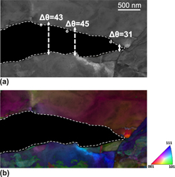
Wetting by liquid sodium and fracture path analysis of sodium induced embrittlement of 304L stainless steel
-
- Journal:
- Journal of Materials Research / Volume 33 / Issue 2 / 29 January 2018
- Published online by Cambridge University Press:
- 27 November 2017, pp. 121-129
- Print publication:
- 29 January 2018
-
- Article
- Export citation
JMR volume 32 issue 22 Cover and Back matter
-
- Journal:
- Journal of Materials Research / Volume 32 / Issue 22 / 28 November 2017
- Published online by Cambridge University Press:
- 24 November 2017, pp. b1-b4
- Print publication:
- 28 November 2017
-
- Article
-
- You have access
- Export citation

Mechanical and microstructural characterization of magnesium single crystals
-
- Journal:
- Journal of Materials Research / Volume 32 / Issue 22 / 28 November 2017
- Published online by Cambridge University Press:
- 24 November 2017, pp. 4196-4205
- Print publication:
- 28 November 2017
-
- Article
- Export citation
-
This study describes results from mechanical tests conducted on magnesium single crystals in comparison with polycrystalline magnesium. It was found by impact testing that the magnesium single crystal is highly ductile due to energy absorption by twinning and slip, while the polycrystalline samples fracture easily upon impact. Compressive testing along two orthogonal directions at low plastic strains was also performed. The microstructure studies by electron backscatter diffraction and XRD pole figure analysis revealed profuse ( $10\overline12$ ) twinning when compression is done along the growth plane (72 16 $\overline {88}$ 62). The twinning and interaction between different twin modes resulted in incipient recrystallization at strains as low as 8% at room temperature. Compression along the nearly orthogonal plane (2 2 $\bar{4}$ 15) was marked by a much lower degree of both twinning and recrystallization. The variation in microstructural response with the orientation of loading allows for a wide range for tailoring mechanical properties of pure magnesium single crystals without any need of alloying.


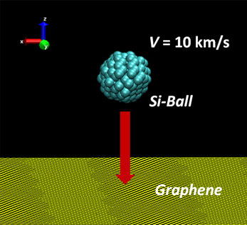
Anomalous characteristics of pore formation in Graphene induced by Si-nanoparticle bombardment
-
- Journal:
- MRS Communications / Volume 7 / Issue 4 / December 2017
- Published online by Cambridge University Press:
- 24 November 2017, pp. 840-847
- Print publication:
- December 2017
-
- Article
- Export citation
JMR volume 32 issue 22 Cover and Front matter
-
- Journal:
- Journal of Materials Research / Volume 32 / Issue 22 / 28 November 2017
- Published online by Cambridge University Press:
- 24 November 2017, pp. f1-f5
- Print publication:
- 28 November 2017
-
- Article
-
- You have access
- Export citation
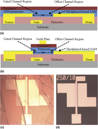
Flexible solution-processed high-voltage organic thin film transistor
-
- Journal:
- Journal of Materials Research / Volume 33 / Issue 2 / 29 January 2018
- Published online by Cambridge University Press:
- 23 November 2017, pp. 149-160
- Print publication:
- 29 January 2018
-
- Article
- Export citation
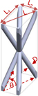
Analytical models of the geometric properties of solid and hollow architected lattice cellular materials
-
- Journal:
- Journal of Materials Research / Volume 33 / Issue 3 / 14 February 2018
- Published online by Cambridge University Press:
- 23 November 2017, pp. 264-273
- Print publication:
- 14 February 2018
-
- Article
- Export citation

Effect of sterilization processes on the properties of a silane hybrid coating applied to Ti6Al4V alloy
-
- Journal:
- Journal of Materials Research / Volume 33 / Issue 2 / 29 January 2018
- Published online by Cambridge University Press:
- 21 November 2017, pp. 161-177
- Print publication:
- 29 January 2018
-
- Article
- Export citation
Transmission electron microscopy with atomic resolution under atmospheric pressures
-
- Journal:
- MRS Communications / Volume 7 / Issue 4 / December 2017
- Published online by Cambridge University Press:
- 21 November 2017, pp. 798-812
- Print publication:
- December 2017
-
- Article
- Export citation

Construction of direct solid-state Z-scheme g-C3N4/BiOI with improved photocatalytic activity for microcystin-LR degradation
-
- Journal:
- Journal of Materials Research / Volume 33 / Issue 2 / 29 January 2018
- Published online by Cambridge University Press:
- 21 November 2017, pp. 201-212
- Print publication:
- 29 January 2018
-
- Article
- Export citation

N-Phenyl naphthalene diimide pendant polymer as a charge storage material with high rate capability and cyclability
-
- Journal:
- MRS Communications / Volume 7 / Issue 4 / December 2017
- Published online by Cambridge University Press:
- 20 November 2017, pp. 967-973
- Print publication:
- December 2017
-
- Article
- Export citation
Development of tensile-compressive asymmetry free magnesium based composite using TiO2 nanoparticles dispersion
-
- Journal:
- Journal of Materials Research / Volume 33 / Issue 2 / 29 January 2018
- Published online by Cambridge University Press:
- 20 November 2017, pp. 130-137
- Print publication:
- 29 January 2018
-
- Article
- Export citation
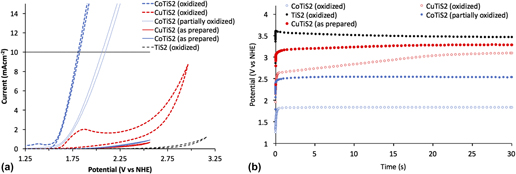
Intercalation makes the difference with TiS2: Boosting electrocatalytic water oxidation activity through Co intercalation
-
- Journal:
- Journal of Materials Research / Volume 33 / Issue 5 / 14 March 2018
- Published online by Cambridge University Press:
- 16 November 2017, pp. 528-537
- Print publication:
- 14 March 2018
-
- Article
-
- You have access
- HTML
- Export citation
Tables
-
- Book:
- Photovoltaic Science and Technology
- Published online:
- 05 July 2018
- Print publication:
- 15 November 2017, pp xxiii-xxvi
-
- Chapter
- Export citation
2 - Crystalline Silicon Cells
-
- Book:
- Photovoltaic Science and Technology
- Published online:
- 05 July 2018
- Print publication:
- 15 November 2017, pp 31-65
-
- Chapter
- Export citation
8 - Characterization, Testing and Reliability of Solar PV Module
-
- Book:
- Photovoltaic Science and Technology
- Published online:
- 05 July 2018
- Print publication:
- 15 November 2017, pp 259-319
-
- Chapter
- Export citation
Index
-
- Book:
- Photovoltaic Science and Technology
- Published online:
- 05 July 2018
- Print publication:
- 15 November 2017, pp 401-412
-
- Chapter
- Export citation
Frontmatter
-
- Book:
- Photovoltaic Science and Technology
- Published online:
- 05 July 2018
- Print publication:
- 15 November 2017, pp i-iv
-
- Chapter
- Export citation
7 - Manufacture of Solar PV Modules
-
- Book:
- Photovoltaic Science and Technology
- Published online:
- 05 July 2018
- Print publication:
- 15 November 2017, pp 203-258
-
- Chapter
- Export citation
3 - Thin Film Solar Cells
-
- Book:
- Photovoltaic Science and Technology
- Published online:
- 05 July 2018
- Print publication:
- 15 November 2017, pp 66-96
-
- Chapter
- Export citation
