Refine search
Actions for selected content:
106117 results in Materials Science
Contents
-
- Book:
- Photovoltaic Science and Technology
- Published online:
- 05 July 2018
- Print publication:
- 15 November 2017, pp vii-x
-
- Chapter
- Export citation
1 - Introduction to Solar Energy and Solar Photovoltaics
-
- Book:
- Photovoltaic Science and Technology
- Published online:
- 05 July 2018
- Print publication:
- 15 November 2017, pp 1-30
-
- Chapter
- Export citation
6 - Manufacture of c-Si and III-V-based High Efficiency Solar PV Cells
-
- Book:
- Photovoltaic Science and Technology
- Published online:
- 05 July 2018
- Print publication:
- 15 November 2017, pp 158-202
-
- Chapter
- Export citation
10 - Design and Implementation of Off-Grid and On-Grid SPV Systems
-
- Book:
- Photovoltaic Science and Technology
- Published online:
- 05 July 2018
- Print publication:
- 15 November 2017, pp 358-400
-
- Chapter
- Export citation
Dedcation
-
- Book:
- Photovoltaic Science and Technology
- Published online:
- 05 July 2018
- Print publication:
- 15 November 2017, pp v-vi
-
- Chapter
- Export citation
4 - III-V Compound, Concentrator and Photoelectrochemical Cells
-
- Book:
- Photovoltaic Science and Technology
- Published online:
- 05 July 2018
- Print publication:
- 15 November 2017, pp 97-133
-
- Chapter
- Export citation
9 - Overview of Solar PV System Technology and Design
-
- Book:
- Photovoltaic Science and Technology
- Published online:
- 05 July 2018
- Print publication:
- 15 November 2017, pp 320-357
-
- Chapter
- Export citation
Figures
-
- Book:
- Photovoltaic Science and Technology
- Published online:
- 05 July 2018
- Print publication:
- 15 November 2017, pp xi-xxii
-
- Chapter
- Export citation
5 - Organic and Polymer Solar Cells
-
- Book:
- Photovoltaic Science and Technology
- Published online:
- 05 July 2018
- Print publication:
- 15 November 2017, pp 134-157
-
- Chapter
- Export citation
Preface
-
- Book:
- Photovoltaic Science and Technology
- Published online:
- 05 July 2018
- Print publication:
- 15 November 2017, pp xxvii-xxx
-
- Chapter
- Export citation
Acknowledgments
-
- Book:
- Photovoltaic Science and Technology
- Published online:
- 05 July 2018
- Print publication:
- 15 November 2017, pp xxxi-xxxii
-
- Chapter
- Export citation
JMR volume 32 issue 21 Cover and Back matter
-
- Journal:
- Journal of Materials Research / Volume 32 / Issue 21 / 14 November 2017
- Published online by Cambridge University Press:
- 13 November 2017, pp. b1-b5
- Print publication:
- 14 November 2017
-
- Article
-
- You have access
- Export citation
JMR volume 32 issue 21 Cover and Front matter
-
- Journal:
- Journal of Materials Research / Volume 32 / Issue 21 / 14 November 2017
- Published online by Cambridge University Press:
- 13 November 2017, pp. f1-f5
- Print publication:
- 14 November 2017
-
- Article
-
- You have access
- Export citation
Introduction
-
- Journal:
- Journal of Materials Research / Volume 32 / Issue 21 / 14 November 2017
- Published online by Cambridge University Press:
- 13 November 2017, pp. 3921-3923
- Print publication:
- 14 November 2017
-
- Article
- Export citation

Creep behavior of a γ′-strengthened Co-base alloy with zero γ/γ′-lattice misfit at 800 °C, 196 MPa
-
- Journal:
- Journal of Materials Research / Volume 32 / Issue 24 / 28 December 2017
- Published online by Cambridge University Press:
- 09 November 2017, pp. 4466-4474
- Print publication:
- 28 December 2017
-
- Article
- Export citation

Fabrication of Mn-CeOx /polyphenylene sulfide functional composites by an in situ reaction for low-temperature NO reduction with NH3
-
- Journal:
- MRS Communications / Volume 7 / Issue 4 / December 2017
- Published online by Cambridge University Press:
- 09 November 2017, pp. 933-937
- Print publication:
- December 2017
-
- Article
- Export citation

Microstructure characterization and phase field analysis of dendritic crystal growth of γ-U and BCC-Mo dendrite in U–33 at.% Mo fast reactor fuel
-
- Journal:
- Journal of Materials Research / Volume 33 / Issue 2 / 29 January 2018
- Published online by Cambridge University Press:
- 09 November 2017, pp. 225-238
- Print publication:
- 29 January 2018
-
- Article
- Export citation

Increased piezoelectric response in functional nanocomposites through multiwall carbon nanotube interface and fused-deposition modeling three-dimensional printing
-
- Journal:
- MRS Communications / Volume 7 / Issue 4 / December 2017
- Published online by Cambridge University Press:
- 08 November 2017, pp. 960-966
- Print publication:
- December 2017
-
- Article
- Export citation
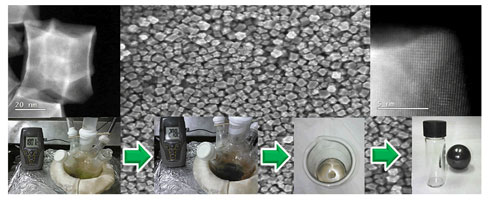
Influence of the injection temperature on the size of Ni–Pt polyhedral nanoparticles synthesized by the hot-injection method
-
- Journal:
- MRS Communications / Volume 7 / Issue 4 / December 2017
- Published online by Cambridge University Press:
- 08 November 2017, pp. 947-952
- Print publication:
- December 2017
-
- Article
- Export citation

Ice-templated silicon foams with aligned lamellar channels
-
- Journal:
- MRS Communications / Volume 7 / Issue 4 / December 2017
- Published online by Cambridge University Press:
- 08 November 2017, pp. 928-932
- Print publication:
- December 2017
-
- Article
- Export citation
