Refine search
Actions for selected content:
106117 results in Materials Science

Characterization of irradiation defect structures and densities by transmission electron microscopy
-
- Journal:
- Journal of Materials Research / Volume 30 / Issue 9 / 14 May 2015
- Published online by Cambridge University Press:
- 13 February 2015, pp. 1195-1201
- Print publication:
- 14 May 2015
-
- Article
- Export citation

Effect of p-GaN layer on the properties of InGaN/GaN green light-emitting diodes
-
- Journal:
- Journal of Materials Research / Volume 30 / Issue 4 / 28 February 2015
- Published online by Cambridge University Press:
- 13 February 2015, pp. 477-483
- Print publication:
- 28 February 2015
-
- Article
- Export citation

Investigation of flowing liquid zinc erosion and corrosion properties of the Fe–B alloy at various times
-
- Journal:
- Journal of Materials Research / Volume 30 / Issue 5 / 14 March 2015
- Published online by Cambridge University Press:
- 13 February 2015, pp. 727-735
- Print publication:
- 14 March 2015
-
- Article
- Export citation
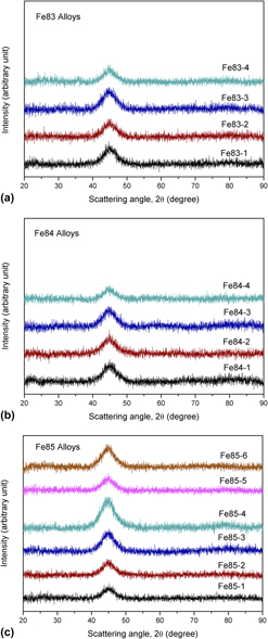
Syntheses and corrosion behaviors of Fe-based amorphous soft magnetic alloys with high-saturation magnetization near 1.7 T
-
- Journal:
- Journal of Materials Research / Volume 30 / Issue 4 / 28 February 2015
- Published online by Cambridge University Press:
- 13 February 2015, pp. 547-555
- Print publication:
- 28 February 2015
-
- Article
- Export citation
Laser liftoff of gallium arsenide thin films
-
- Journal:
- MRS Communications / Volume 5 / Issue 1 / March 2015
- Published online by Cambridge University Press:
- 12 February 2015, pp. 1-5
- Print publication:
- March 2015
-
- Article
- Export citation
Copyright page
-
- Book:
- Amorphous Semiconductors
- Published online:
- 05 February 2015
- Print publication:
- 12 February 2015, pp iv-iv
-
- Chapter
- Export citation
3 - Structure
-
- Book:
- Amorphous Semiconductors
- Published online:
- 05 February 2015
- Print publication:
- 12 February 2015, pp 24-85
-
- Chapter
- Export citation
2 - Preparation techniques
-
- Book:
- Amorphous Semiconductors
- Published online:
- 05 February 2015
- Print publication:
- 12 February 2015, pp 14-23
-
- Chapter
- Export citation
Contents
-
- Book:
- Amorphous Semiconductors
- Published online:
- 05 February 2015
- Print publication:
- 12 February 2015, pp vii-viii
-
- Chapter
- Export citation
Amorphous Semiconductors - Title page
-
-
- Book:
- Amorphous Semiconductors
- Published online:
- 05 February 2015
- Print publication:
- 12 February 2015, pp iii-iii
-
- Chapter
- Export citation
Index
-
- Book:
- Amorphous Semiconductors
- Published online:
- 05 February 2015
- Print publication:
- 12 February 2015, pp 145-147
-
- Chapter
- Export citation
4 - Electronic structure
-
- Book:
- Amorphous Semiconductors
- Published online:
- 05 February 2015
- Print publication:
- 12 February 2015, pp 86-116
-
- Chapter
- Export citation
Analysis of preferential orientation in zirconium samples deformed by uniaxial tension using neutron and X-ray diffraction
-
- Journal:
- Powder Diffraction / Volume 30 / Issue S1 / June 2015
- Published online by Cambridge University Press:
- 12 February 2015, pp. S52-S55
-
- Article
- Export citation
-
Two series of zirconium samples were investigated by neutron and X-ray diffraction. First series of the samples was deformed at room temperature (RT), whereas the second series was deformed at 300 °C. Both series were deformed on uniaxial tensile machine INSTRON 5882 from strain 0 to 30% (strain step was 5%). The neutronographic texture measurements were performed on the KSN-2 neutron diffractometer located at the research reactor LVR-15 in the Nuclear Research Institute, plc. Rez, Czech Republic. The X-ray measurements were performed at the theta/theta X'Pert PRO diffractometer with the Cr X-ray tube. Observed data were processed by the software packages GSAS and X'Pert Texture. Preferential orientation of the $\left({10\bar 10} \right)$ and $\left({11\bar 20} \right)$ plane poles is found to be parallel to the rolling direction for both tested deformation series. Poles of the $\lpar 10\bar 12\rpar $ and $\lpar 10\bar 13\rpar $ planes tend to be parallel to the normal direction (Tables II and III). Orientation of the basal poles is tilted by 45° from the normal direction toward the transverse direction. Sharpness of the resulting texture increases with extends of the applied deformation as well as with rise of the tensile test temperature from the RT level to 300 °C.


Dedication
-
- Book:
- Amorphous Semiconductors
- Published online:
- 05 February 2015
- Print publication:
- 12 February 2015, pp v-vi
-
- Chapter
- Export citation
Amorphous Semiconductors - Half title page
-
- Book:
- Amorphous Semiconductors
- Published online:
- 05 February 2015
- Print publication:
- 12 February 2015, pp i-ii
-
- Chapter
- Export citation

Production of aluminum nitride from aluminum metal using molten fluoride
-
- Journal:
- Journal of Materials Research / Volume 30 / Issue 5 / 14 March 2015
- Published online by Cambridge University Press:
- 12 February 2015, pp. 635-644
- Print publication:
- 14 March 2015
-
- Article
- Export citation
5 - Photoinduced phenomena
-
- Book:
- Amorphous Semiconductors
- Published online:
- 05 February 2015
- Print publication:
- 12 February 2015, pp 117-144
-
- Chapter
- Export citation

Damage accumulation in diamond during ion implantation
-
- Journal:
- Journal of Materials Research / Volume 30 / Issue 9 / 14 May 2015
- Published online by Cambridge University Press:
- 12 February 2015, pp. 1583-1592
- Print publication:
- 14 May 2015
-
- Article
- Export citation
Preface
-
- Book:
- Amorphous Semiconductors
- Published online:
- 05 February 2015
- Print publication:
- 12 February 2015, pp ix-xii
-
- Chapter
- Export citation
1 - Introduction
-
- Book:
- Amorphous Semiconductors
- Published online:
- 05 February 2015
- Print publication:
- 12 February 2015, pp 1-13
-
- Chapter
- Export citation
