To save content items to your account,
please confirm that you agree to abide by our usage policies.
If this is the first time you use this feature, you will be asked to authorise Cambridge Core to connect with your account.
Find out more about saving content to .
To save content items to your Kindle, first ensure no-reply@cambridge.org
is added to your Approved Personal Document E-mail List under your Personal Document Settings
on the Manage Your Content and Devices page of your Amazon account. Then enter the ‘name’ part
of your Kindle email address below.
Find out more about saving to your Kindle.
Note you can select to save to either the @free.kindle.com or @kindle.com variations.
‘@free.kindle.com’ emails are free but can only be saved to your device when it is connected to wi-fi.
‘@kindle.com’ emails can be delivered even when you are not connected to wi-fi, but note that service fees apply.
We report an easy way to assemble porous one-dimensional (1D) Ni2P nanowires through phosphatization of a Ni(SO4)0.3(OH)1.4 nanobelt precursor. The peculiar synthetic process endows the Ni2P nanowires with large surface area, hierarchical porous structure and the ability to form closely connected network for transporting both electrons and electrolytes, which in conjunction with the high intrinsic electrocatalytic activity make it an excellent low-cost counter electrode material for dye-sensitized solar cells (DSSCs). Indeed, the first investigation of such novel counter electrode for DSSC presented superb photovoltaic performance rivaling the conventional Pt counter electrode.
We report a systematic investigation of the thermoelectric properties of n-type Ga-doped ZnO synthesized using different ball milling conditions. Samples fabricated by the high-energy ball milling resulted in a highly dense layered structure with randomly distributed voids. These samples measured the lowest room temperature thermal conductivity, i.e., 27 W/mK due to increased phonon scattering. Furthermore, the Ga:ZnO system showed a metal–semiconductor transition above 300 K with transition temperature decreasing with increasing doping level. Measurement of the activation energy revealed the presence of one donor level around 3.9–7.8 meV and a deeper donor level around 15.4–18.1 meV below the conduction band for the Ga-doped samples. For Ga-doped ZnO, Seebeck coefficient of −185 μV/K (at 1000 K) was achieved, which is ∼30–45% higher than the values previously reported for Zn:Ga system. Jonker plot analysis was used to analyze the scope of Ga:ZnO bulk system.
To understand the impact that the growth rate has on the residual stress of chemical vapor deposition-grown 3C–SiC heteroepitaxial films on Si substrates, growth experiments were performed. The film thickness was held constant at ∼2.5 μm independent of the growth rate so as to allow for direct film comparison as a function of the growth rate. Stress analysis performed by profilometer curvature measurement, μιχρο-Raman shift analysis and micro-machined freestanding structures, show an apparent disagreement about the stress nature. This incongruity between the experimental data can be explained assuming a strong stress field located in the substrate related to defects generated in the silicon during the growth process.
The synthesis, structure, and electrical performances of titanium dioxide (TiO2 and also doped TiO2) thin films, a capacitor dielectric for dynamic random access memory (DRAM) and a resistance switching material in resistance switching RAM (ReRAM), are reviewed. The three-dimensionality of these structures and the extremely small feature sizes (<20 nm) of these memory devices require the synthesis method of TiO2-based layers to exhibit high degree of conformality. Atomic layer deposition is, therefore, the method of choice in respect of film growth for these applications. The unique arrangement of the TiO6-octahedra in the rutile structure, which results in the value for dielectric constant of the dielectric layer, εr (>100), makes the material especially attractive as the capacitor dielectric layer in DRAM. Removing some of the oxygen ions from the rutile structure and arranging the resulting oxygen vacancies on a specific crystallographic plane results in the so called Magnéli phase materials, which show distinctive conducting semiconductor or metallic characteristics. External electrical stimuli can cause the repeated formation and rupture of conducting channels that consist of these Magnéli phase materials in the insulating TiO2 matrix, and this aspect makes the material a very feasible choice for applications in ReRAM. This article reviews the material properties, fabrication process, integration issues, and prospect of TiO2 films for these applications.
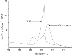
To replace ternary polymer with binary polymer, a novel bifunctional comonomer β-methylhydrogen itaconate (MHI) was synthesized to prepare poly(acrylonitrile-co-β-methylhydrogen itaconate) [P(AN-co-MHI)] copolymer used for carbon fiber precursor. The structural evolution and stabilization mechanism of P(AN-co-MHI) and polyacrylonitrile (PAN) during stabilization were studied by Fourier transform infrared spectroscopy, x-ray diffraction, differential scanning calorimetry, thermogravimetry, and kinetic investigation. The activation energy (Ea) of the stabilization reactions were calculated by Kissinger method and Ozawa method. The results show that the P(AN-co-MHI) exhibits a lower stabilization temperature than terpolymers containing similar chemistry component and a significantly improved stabilization performance compared with PAN homopolymer, such as lower cyclization temperature, lower Ea (85.36 kJ/mol), and larger extent of stabilization under the same condition, which is mainly attributed to the initiation of MHI comonomer through an ionic cyclization mechanism. The dehydrogenation of P(AN-co-MHI) is also promoted by the incorporation of comonomer MHI into PAN chains. Simultaneously, the rheological analysis shows that P(AN-co-MHI) possesses better spinnability than PAN, which is beneficial for preparation of high performance carbon fiber.
Using titanium sulfate, Ti(SO4)2, as precursor and sodium hydroxide, NaOH, as adjusting reagent, pure brookite, pure anatase, and mixed-phase titanium dioxide (TiO2) with tunable brookite/anatase ratios were synthesized via a hydrothermal process. The samples were characterized by x-ray diffractionspectrometry, ultraviolet-visible diffuse reflectance spectrometry, transmission electron microscopy, and Brunauer-Emmett-Teller measurement. Photocatalytic degradation of Rhodamine B in aqueous solution served as a probe reaction to evaluate the photocatalytic activity of the as-prepared nanocomposites under visible irradiation (λ > 400 nm). The mixed-phase TiO2 exhibits higher photodegradation activity than single phase TiO2. The sample with 63.1% brookite and 36.9% anatase shows the highest degradation activity. Possible mechanism attributing to the enhanced activity was proposed based on the strucutre and surface property of the samples.
Applying a first-principles computational approach, we study the electronic and charge transport properties of the interfaces between metals and capped carbon nanotubes (CNTs) with various arrangements of topological defects. Observing the length scaling of resistance, we first show that capped CNTs exhibit only one CNT-body-determined low-slope scaling and the resulting very low long-length-limit resistance. The intrinsically low resistance (absence of Schottky-barrier-dominated high-slope scaling) of capped CNTs is next analyzed by the local density of states, which shows the formation of unusual propagating-type metal-induced gap states originating from the topological defect states that are well connected with CNT edge and body states.
In this study, Au/aminosilica composite nanospheres have been synthesized via a simple one-pot route using HAuCl4 and N-(3-trimethoxysilylpropyl)-ethylenediamine as starting materials. Scanning electron microscopy results show that these spheres are with diameters of about 300 nm. The obtained Au/aminosilica nanospheres were used as nonviral carriers for gene delivery. Compared with commercial Lipofectamine 2000, the Au/aminosilica nanospheres are with higher transfection efficiency and lower cytotoxicity. Furthermore, the nanospheres are biocompatible, which may find applications in gene delivery and drug carrier.
We report herein the crystal growth of ZnO nanoparticles by the foam fractionation method. In this study, the vertical column height of the foam was fixed and the velocity of the sparging air was varied, and the effect of foam flow rate on the synthesis of ZnO was investigated. The obtained ZnO consisted of aggregated platelets and had differing ultraviolet absorbances. The as-synthesized ZnO was hydrophobic because of the interaction between the anionic head groups of sodium dodecyl sulfate (SDS) and the ZnO under the precipitation conditions. The long chain of the SDS molecule was the cause of hydrophobicity. The contact angle of water was in the range of 95–105° for the obtained ZnO/SDS surface. The photocatalytic degradation efficiency of the as-synthesized (ZnO/SDS) and the calcined ZnO was investigated for methylene blue, and the calcined ZnO retained its activity even after three recycles.
Fabrication of nanosized silicon carbide (SiC) crystals is a crucial step in many biomedical applications. Here we report an effective fabrication method of SiC nanocrystals based on simple electroless wet chemical etching of crystalline cubic SiC. Comparing an open reaction system with a closed reaction chamber, we found that the latter produces smaller nanoparticles (less than 8 nm diameter) with higher yield. Our samples show strong violet-blue emission in the 410–450 nm region depending on the solvents used and the size. Infrared measurements unraveled that the surface of the fabricated nanoparticles is rich in oxidized carbon. This may open an opportunity to use standard chemistry methods for further biological functionalization of such nanoparticles.
Cu–In–Ga precursor thin films were deposited onto soda lime glass by magnetron cosputtering CuIn and CuGa alloy targets. After that, Cu(In,Ga)Se2(CIGSe) absorbers were formed by selenizing those alloy precursors with Se vapor at 550 °C. The influence of the precursor temperature on the properties of CIGSe thin film was investigated. The results show that a lot of pinholes existed in the CIGSe thin film produced by selenizing the Cu–In–Ga alloy precursor, which was sputtering deposited at ambient temperature. After sputtering substrate temperature of 250 °C was applied, pinholes were avoided. The surface roughness of Cu–In–Ga precursor increased with the increase of sputtering substrate temperature. Due to the volume expansion of selenization process, even the precursor with high surface roughness could be converted to smooth and compact CIGSe thin film.
Normal spectral intensities of resistively heated preoxidized ZrB2–30 mol% SiC–6 mol% B4C specimens were measured in the 1–6 μm and ∼1100–1500 °C ranges. Using Wein’s displacement law, the temperatures of these specimens were determined, in turn permitting calculation of normal spectral emittances using Planck’s law. Spectral emittance data were affected by absorption/emission of H2O/CO2 gases; total emittances were determined from the averages of data in spectral ranges devoid of gaseous interference. Total emittances decreased from 1.0 at 1100 °C to 0.8 at 1500 °C. This trend is consistent with the behavior expected of a dielectric coating.
This paper presents the results of a combined experimental, theoretical, and computational study of the adhesion between suspended polymeric films and a substrate in a model drug-eluting stent. Atomic force microscope is used to measure the pull-off force between the polymer and the substrate. The adhesion energy was then obtained from the measured pull-off forces and adhesion theories. Subsequently, the adhesion energy was incorporated into interfacial fracture mechanics zone model that was used to determine mode mixity dependence of the interfacial fracture toughness. The mode mixity-dependent fracture toughness conditions were then integrated into finite element models that were used to compute the critical push-out force of the suspended polymeric films. The predicted push-out forces were in good agreement with the results obtained from the experiments.
A method of growing SiC nanowires (NWs) on 4H–SiC surfaces by in situ vapor-phase catalyst delivery was developed as an alternative to the ex situ deposition of the metal catalyst on the targeted surfaces before the NW chemical vapor deposition (CVD) growth. In the proposed method, sublimation of the catalyst from a metal source placed in the hot zone of the CVD reactor, followed by condensation of the catalyst-rich vapor on bare substrate surface was used to form the catalyst nanoparticles required for the vapor–liquid–solid (VLS) growth of SiC NWs. The NW density was found to gradually decrease downstream from the catalyst source and was influenced by both the gas flow rate and by the catalyst diffusion through the boundary layer above the catalyst source. Formation of poly-Si islands at too low value of the C/Si ratio created preferential nucleation centers for misaligned SiC NWs and NW bushes. The flexibility of controlling the nanoparticle density made this technique suitable for NW growth on horizontal surfaces as well as on patterned SiC substrates, including the vertical sidewalls of SiC mesas.