To save content items to your account,
please confirm that you agree to abide by our usage policies.
If this is the first time you use this feature, you will be asked to authorise Cambridge Core to connect with your account.
Find out more about saving content to .
To save content items to your Kindle, first ensure no-reply@cambridge.org
is added to your Approved Personal Document E-mail List under your Personal Document Settings
on the Manage Your Content and Devices page of your Amazon account. Then enter the ‘name’ part
of your Kindle email address below.
Find out more about saving to your Kindle.
Note you can select to save to either the @free.kindle.com or @kindle.com variations.
‘@free.kindle.com’ emails are free but can only be saved to your device when it is connected to wi-fi.
‘@kindle.com’ emails can be delivered even when you are not connected to wi-fi, but note that service fees apply.
Enhanced and confined optical fields near metallic nanostructures, supporting surface plasmon (SP) resonances, make it possible to enhance the interaction of light with tiny amounts of matter, down to the molecular level. Such capability has been extensively exploited in the framework of optical spectroscopy, nonlinear optics, imaging and integrated optics, among others. Here we discuss the use of plasmonics for optical trapping. Plasmon-based trapping addresses key limitations of conventional optical tweezers formed at the focus of a diffraction-limited laser beam. Beyond permitting trapping of smaller objects, down to the true nanometer scale, they enable parallel trapping from a single beam and can be easily integrated on a chip. SP-based trapping opens new perspectives in a wide range of fields from biology to quantum optics.
Emerging telecommunication and data routing applications anticipate a photonic roadmap leading to ultra-compact photonic integrated circuits. Consequently, photonic devices will soon have to meet footprint and efficiency requirements similar to their electronic counterparts calling for extreme capabilities to create, guide, modulate, and detect deep-subwavelength optical fields. For active devices such as modulators, this means fulfilling optical switching operations within light propagation distances of just a few wavelengths. Plasmonics, or metal optics, has emerged as one potential solution for integrated on-chip circuits that can combine both high operational speeds and ultra-compact architectures rivaling electronics in both speed and critical feature sizes. This article describes the current status, challenges, and future directions of the various components required to realize plasmonic integrated circuitry.
When an electron beam passes through or near a metal structure, it will excite surface plasmons, providing a unique way to access surface plasmon behavior at the nanoscale. An electron beam focused to nanometer dimensions thus functions as a point source that is able to probe the local plasmonic mode structure at deep-subwavelength resolution. In this article, we show how well-controlled coupling between an electron beam and surface plasmons, combined with a far-field detection system, allows characterization and manipulation of plasmons on a variety of plasmonic devices. By mapping the spatial profile of inelastic scattering to resonant modes, the dispersion and losses of surface plasmons are resolved. The technique further allows probing of the confinement of plasmons within cavities and measuring the angular emission profile of nanoantennas. The coupling of electrons to surface plasmons allows the use of the electron beam as a dipole emitter that can be positioned at will. The beam position thereby can select between modes with different symmetries. This effect can be used to exert forces on plasmonic structures on the nanometer length scale with great control.
Surface plasmon polaritons, combined excitations of light and free electrons of a metal, have emerged as an alternative information carrier for nanoscale circuitry due to their ability to confine light far below the size of the wavelength. They hold the potential to act as a revolutionary bridge between current diffraction-limited microphotonics and bandwidth-limited nanoelectronics. Interestingly, the nanoscale confinement achievable by plasmons also increases the interaction with quantum emitters, paving the way for quantum applications. Exotic non-classical properties of light such as entanglement and squeezing can be embedded into plasmons and faithfully transmitted and received. Recently, it was also shown that unique coupled plasmonic excitations can be engineered on the nanoscale with artificial media (metamaterials) to enhance and control light-matter interaction. A major departure from the conventional classical description of the plasmon is under development. The aim is to incorporate the “wave” nature of matter manifested in ultra-small metallic nanoparticles and the “particle” nature of light, which can play a role in future integrated circuits with capabilities of quantum information processing. This article reviews developments in the field of quantum nanophotonics, an exciting frontier of plasmonic applications ranging from single photon sources and quantum information transfer to single molecule sensing.
Next-generation fission and fusion nuclear reactor materials will be exposed to very high temperatures, intense neutron radiation, corrosive environments, and, mostly, all three at once. Grand opening will be given to the material, if they have stability at high temperature operating favorable in the extreme environments, self-healing, thermal as well as irradiation properties. Owing to the superior properties of silicon carbide, nuclear scientists are closely evaluating SiC-based materials for various applications in nuclear reactors. In the present perspective, relevant properties, challenging issues, and recommendations are emphasized. Based on our recent experiments, attempt to solve various uses on SiC-based materials in nuclear applications is described in detail.
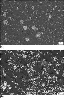
Systematic studies have been carried out for investigating the mechanical properties of carbon nanotube (CNT)-reinforced phenolic resin. In this work, phenolic resin/CNT nanocomposite were processed using two different techniques: (i) three-roll calender device (TRC) and (ii) aqueous solution processes. In both techniques, up to 2 wt% CNT was used. In this study, it was observed that the values of tensile strength, Young’s modulus, shear stress, impact resistance and also that of the tribological properties increased directly proportional to carbon nanotube volume content. Halpin-Tsai, Voigt-Reuss and Cox equations were adopted to fit the experimental data of the tensile strength and Young’s modulus of the multiwalled carbon nanotube/phenolic resin composite. Morphological analysis was done utilizing scanning electron microscopy (SEM) and good dispersion of nanotubes within the phenolic resin matrix was revealed. Also according to the results presented in this work, SEM showed that TRC processing gave better dispersion than aqueous solution mixing. The observation that the values for mechanical properties increased more for TRC than aqueous mixed samples is consistent with this.
Methods for identifying the hardening behavior of solids described by power law through indentation testing have been well developed. However, many important engineering materials deviate from the power law description significantly. After fitting the uniaxial curves of several typical materials, the three-parameter relationship proposed by Voce [E. Voce, J. Inst. Met.74, 537–562 (1948)] is chosen to describe the hardening behavior for its fitting performance and inherent simplicity. Based on the Voce law, an efficient method is formulated to extract the hardening data from a single spherical indentation curve. Improved identifying performance is manifested by applying the method to four metallic materials. It is validated that the present method has the ability to effectively identify the plastic properties of materials through spherical indentation testing.
The numerical approach of Lee et al. [Trans. Korean Soc. Mech. Eng., A28, 816–825 (2004)] to spherical indentation technique for property evaluation of hyperelastic rubber is enhanced. The Yeoh model is adopted as the constitutive form of rubber material because it can express well large deformation and cover various deformation modes with a simple form. We first determine the friction coefficient between a rubber specimen and a spherical indenter in a practical viewpoint and perform finite element simulations for a deeper indentation depth than that selected by Lee et al. [Trans. Korean Soc. Mech. Eng., A28, 816–825 (2004)]. An optimal data acquisition spot is selected, which features sufficiently large strain energy density and negligible frictional effect. We improve then two normalized functions mapping an indentation load–displacement curve onto a strain energy density–invariant curve, the latter of which gives the Yeoh model constants. The enhanced spherical indentation approach successfully produces the rubber material properties with an average error of less than 5%. The validity of our developed approach is verified by experimental evaluation of material properties with three kinds of rubber materials.
In this article, the biofunctionalization of 6H–SiC (0001) surfaces via self-assembled monolayers (SAMs) has been studied as a means to modify the in vitro biocompatibility of this semiconductor substrate with H4 (human neuroglioma) and PC12 (rat pheochromocytoma) cells. Silanization with aminopropyldiethoxymethylsilane (APDEMS) and aminopropyltriethoxysilane (APTES), which provided moderately hydrophilic surfaces, and alkylation with 1-octadecene that produced hydrophobic surfaces were used to control the 6H–SiC surface chemistry and evaluate changes in cell viability and morphology due to these surface modifications. The morphology of the cells was evaluated with atomic force microscopy. In addition, 3-(4,5-dimethylthiazol-2-yl)-2,5-diphenyltetrazolium bromide (MTT) assays were used to quantitatively evaluate the cell viability on the SAM-modified surfaces. In all cases, the cell proliferation was observed to improve with respect to untreated 6H–SiC surfaces, with up to a 2x increase in viability on the 1-octadecene-modified surfaces, up to 6x increase with APDEMS-modified surfaces, and up to 8x increase with APTES-modified surfaces. This proves the potential of SiC as a substrate for medical devices given the possibility to tailor its surface chemistry for specific applications.
Solid solutions of Ba1−xPbxZrO3 (0 ≤ x ≤ 0.75) have been synthesized successfully by polymeric citrate precursor method for the first time. The solid solutions were characterized by powder x-ray diffraction (XRD), scanning electron microscopy, transmission electron microscopy, and surface area studies. XRD studies reveal the monophasic nature of these highly crystalline nanoparticles (except few impurity of ZrO2 in PbZrO3). Lattice parameter of Ba1−xPbxZrO3 (0.20 ≤ x ≤ 0.75) decreases with increasing the Pb content. Dielectric properties of these nanoparticles were investigated as a function of frequency and temperature. The dielectric constant for x = 0.15 showed a maximum value of 75.5.
Observation of room temperature ferromagnetism (RTFM) is reported in polycrystalline thin films of Ti1−xMnxO2 (x = 0.10 and 0.15) synthesized by spray pyrolysis technique on fused quartz substrates. Our experimental results clearly suggest partial incorporation of manganese (Mn) in titanium dioxide (TiO2) lattice up to certain extent and rest of the Mn ions are consumed to form secondary Mn-related phase such as manganese oxide (Mn3O4). The observed weak ferromagnetic ordering at room temperature in the films is established to be due to incorporation of Mn in TiO2matrix rather than the presence of other secondary phases since none of the Mn or Ti/Mn oxide phase is ferromagnetic at room temperature. Bound magnetic polaron model is invoked to explain the observed ferromagnetism in these highly resistive films.
Multiwalled carbon nanotubes (MWCNTs) obtained using ethylene as a carbon source and nanocrystalline iron as a catalyst were used as the initial material. The functionalization of MWCNTs was carried out using chlorine in the liquid and gas phase. In the second case, the reaction was conducted in the temperature range from 50 to 450 °C for 2 h. The presence of chlorine species on the surface of chlorinated samples was confirmed by x-ray photoelectron spectroscopy (XPS). A quantitative analysis of metal impurity content was validated by means of thermogravimetric analysis. Better results of metal removal were achieved when the chlorination process was conducted in the gas phase and the ratio of metal in samples amounted from 2.3% to 5.1%.