To save content items to your account,
please confirm that you agree to abide by our usage policies.
If this is the first time you use this feature, you will be asked to authorise Cambridge Core to connect with your account.
Find out more about saving content to .
To save content items to your Kindle, first ensure no-reply@cambridge.org
is added to your Approved Personal Document E-mail List under your Personal Document Settings
on the Manage Your Content and Devices page of your Amazon account. Then enter the ‘name’ part
of your Kindle email address below.
Find out more about saving to your Kindle.
Note you can select to save to either the @free.kindle.com or @kindle.com variations.
‘@free.kindle.com’ emails are free but can only be saved to your device when it is connected to wi-fi.
‘@kindle.com’ emails can be delivered even when you are not connected to wi-fi, but note that service fees apply.
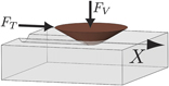
Indentations tests have been performed on two standard materials SiO2 and Si (100) using two Berkovich indenters presenting different tip defects. Estimations of the tip radii deduced from analyses of maximal applied load versus contact depth and stiffness versus contact depth curves have been compared for experimental observation of each indenter tip obtained with atomic force microscopy (AFM). Results indicate that the determination of the tip defect from data extracted form load–displacement curves is partly dependent on the mechanical properties of the tested material. Then, an original study is proposed to evidence the influence of the tip defect on mechanical response during indentation. Experimental AFM observations of the tip indenter geometries have been introduced in finite element software MSC MARC to reproduce indentation tests on bulk material surfaces. We demonstrated at very shallow penetration depth (less than 50 nm) that the real indenter tip defects have to be considered in the simulation runs, especially to identify accurately the rheological parameters of the tested surface.
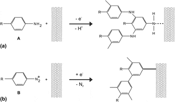
The ability to tune the functional interface of single-walled carbon nanotubes in a versatile manner is key to the success of deploying them as an active material in chemical and biological sensors. Here we present an overview of our device strategies demonstrating the use of controlled electrochemical functionalization to tune this interface by bringing in different functionalities ranging from metallic nanoparticles to biomolecules onto the nanotube surface. The extent of such a functionalization is tunable, providing us with a good control over sensitivity, selectivity, and detection limit of the realized sensors. Moreover, the sensor mechanisms have been analyzed. Taken together the methods and results outlined here constitute a general framework for the rational design of nanoscale field-effect-based chemical sensors and biosensors.
There is much interest in the recent years in the nanoscale metallic multilayered composite materials due to their unusual mechanical properties, such as very high flow strength and stable plastic flow to large strains. These unique mechanical properties have been proposed to result from the interface-dominated plasticity mechanisms in nanoscale composite materials. Studying how the dislocation configurations and densities evolve during deformation will be crucial in understanding the yield, work hardening, and recovery mechanisms in the nanolayered materials. In an effort to shed light on these topics, uniaxial compression experiments on nanoscale Cu/Nb single-crystal multilayer pillars using ex situ synchrotron-based Laue x-ray microdiffraction technique were conducted. Using this approach, we studied the nanoscale Cu/Nb multilayer pillars before and after uniaxial compression to about 14% of plastic strain and found significant Laue peak broadening in the Cu phase, which indicates storage of statistically stored dislocations, while no significant Laue peak broadening was observed in the Nb phase in the nanoscale multilayers. These observations suggest that at 14% plastic strain of the nanolayered pillars, the deformation was dominated by plasticity in the Cu nanolayers and elasticity or possibly a zero net plasticity (due to the possibility of annihilation of interface dislocations) in the Nb nanolayers.
This article presents a novel microscratch technique for the determination of the fracture toughness of materials from scratch data. While acoustic emission and optical imaging devices provide quantitative evidence of fracture processes during scratch tests, the technique proposed here provides a quantitative means to assess the fracture toughness from the recorded forces and depth of penetration. We apply the proposed method to a large range of materials, from soft (polymers) to hard (metal), spanning fracture toughness values over more than two orders of magnitude. The fracture toughness values so obtained are in excellent agreement with toughness values obtained for the same materials by conventional fracture tests. The fact that the proposed microscratch technique is highly reproducible, almost nondestructive, and requires only small material volumes makes this technique a powerful tool for the assessment of fracture properties for microscale materials science and engineering applications.
Interrod regions exist between the enamel rods and are known to have different crystallite orientations and a higher organic content compared to the enamel rods (the intrarod regions). This study aims to characterize the mechanical properties of both regions especially the time-dependent properties by using spherical indentation. Despite the very small amount of proteins, the interrod region shows statistically significantly higher inelastic energy dissipation than the intrarod region with increased deformation times. The total displacement under constant load (creep), viscosity, and stress relaxation behavior of both regions are also reported. Similar to the observation of previous studies, the elastic modulus and hardness in the intrarod region are significantly higher than in the interrod region.
This experimental study presents a comparison of differently tensile stressed silicon nitride (SiN) layers and their response to irradiation in a vacuum ultraviolet (VUV) curing system. Therefore, three types of silicon nitride with initial stress levels of 450 MPa, 700 MPa and 980 MPa were deposited by plasma enhanced chemical vapor deposition (PECVD). In contrast to industrial standard VUV curing with broadband lamps ≥ 220 nm radiation wavelengths, we analyzed the effects of curing with single wavelengths at 172 nm and 222 nm. The samples were characterized by Fourier Transform Infrared Spectroscopy, ellipsometry, and wafer bow measurement. It could be shown that high energy photons are able to dehydrogenize SiN films more than lower energetic photons compared with lower Si-N-Si crosslinking effects. Furthermore, we could show that a dual combined 172 nm and 222 nm VUV curing procedure can produce films with very low hydrogen concentration and high percentage of structural units consisting of Si-N-Si bonds. In conclusion of this study, an up to +900 MPa stress increasing process could be established.
In this work we present the bases to perform investigation on the effects on the morphology and size of nanostructures of silver, owed to the modification of synthesis factors in a polyol process such as temperature, concentration, time of reaction, injection speed and time of injection. It is claimed that control over Ag nanostructures shape could be improved and significant information about the synthesis process can be obtained. The design of experiments was done aimed to obtain useful information about how to yield as much as possible specific structures of interest.
Medium scale integrated circuits with 108 CNT-TFTs have been fabricated using CNTs grown by plasma enhanced chemical vapor deposition (PECVD) which has the advantage of preferential growth of CNTs with semiconducting behavior in the FET current–voltage characteristics. High-speed operation with a switching time of 0.51 μs/gate, which is highest in the CNT-TFT integrated circuits to our knowledge, was demonstrated by a 53-stage ring oscillator. Characterization of CNT-TFTs using scanning probe microscopy has also been performed. The island-like structure in the electrical properties of the CNT network was observed even in a high-density CNT network in the subthreshold regime. This was explained by the decrease of the effective number of CNTs which contribute the electrical conduction.
Environmental, concerns regarding reducing CO2 emissions and the drive of having better fuel economy have already enthused the car manufacturer to use the weight materials having better mechanical properties. Automotive industry has shown a great interest in Dual Phase steels due to the possibility of reducing weight of vehicles and increasing the passenger safety at a very competitive cost. Automotive applications unavoidably entail welding and joining in the manufacturing process and the fatigue resistance of welded joints due to the integrity and safety requirements. The variation of welding parameters (voltage, current and speed of welding) affects weld performance, mechanical, and metallurgical properties.
The CMT (Cold Metal Transfer) braze welding is a relatively new technology that partially decouples the arc electrical transients from the filler wire feed rate. It allows reducing the heat required for welding and permits higher joining speeds.
The aim of this work is to study the interfacial microstructures and intermetallic compounds produced by cold metal transfer welding of two plates of galvanized DP600 dual phase steel with CuSi3 as filler metal. The study was performed by applying a CMT braze welding with three different joining speeds. The welded microstructures and microhardness were determined and related to the welding process conditions.
A small HAZ, constituted by martensite, bainite and coarse ferrite grains, has been highlighted. Furthermore, an intermetallic Fe-Si-Cu compound layer formed at the interface between steel and filler metal. The joining speed sways the size of ZTA since the heat input Q affects the phase transformation in the weld and heat affected zone
This parameter also affects the thickness of the compound layer and the size of precipitates in the filler metal, likewise the mechanical characteristics. The fracture starts at the interface steel-copper where intermetallic compounds formed.
In this paper the spore-crystal complex of Bacillus thuringiensis var. israelensis (Bti) was immobilized by the sol-gel process in a hybrid polymer using as precursors the inorganic tetraethyl orthosilicate (TEOS) and the organic Polydimethylsiloxane (PDMS); in order to combine the advantages of both materials in a hybrid matrix to improve aspects such as the thermal stability, the hydrophobic properties and the porosity. Bti produces different crystals during sporulation phase; these are of protein nature and are used as bio-insecticides. It is important to mention that the insecticide attack is specific to the mosquito larva that causes dengue and black flies. The samples were characterized to ensure viability by performing growth kinetics with fermentations immersed in a flask, this microbial growth was monitored by dry weight, glucose consumption and characterized by Fourier Transform Infrared Spectroscopy (FTIR) to observe the interaction of materials with spore-crystal complex.
Homoepitaxial layers were grown with very low surface roughness on 4", 4˚ off-axis substrates, but a new kind of large obtuse angled triangular defect that spanned 1000-2000 μm was observed. Process changes resulted in reduction of the size and concentration of these triangular defects from 3.5cm-2 to 0.13cm-2. Both large and small triangular defects were found to have a similar core structure. No degradation in the epitaxial morphology or quality was seen due to the process change. JBS diodes fabricated on wafers with large triangular defects had much higher leakage when the triangular defects were present in the active area of the diodes.
The relationship between tortuosity and porosity and its influence on effective transport properties in lithium-ion cells was analyzed. The variation in cell performance with changes in component thicknesses, porosities and tortuosities was investigated. Optimal, novel electrode designs are developed to improve their rate capability even at higher active material loadings.
Understanding factors affecting cell invasion influences the design ofengineered constructs for tissue regeneration. The objective of this workwas to investigate the effect of matrix stiffness on invasion of tumor cellsthrough a synthetic hydrogel with well-defined properties. A novel staracrylate-functionalized polyethylene glycol-co-lactide (SPELA) macromer wassynthesized to produce hydrogels with well-defined water content, elasticmodulus, degree of crosslinking and hydrophilicity. The hydrogel was formedby photo-polymerization of the macromer with or without integrin-bindingcell adhesive RGD peptide. Cell invasion experiments were carried out in atranswell with SPELA hydrogel as the invading matrix and 4T1 mouse breastcancer cells. The invading cells on the lower membrane side were countedwith an inverted fluorescent microscope. The concentration of SPELA macromerranged from 10-25 wt% and that of RGD ranged from 1x10⁻⁴ to 1x10⁻² M. The shear modulus of the hydrogel varied from 200 Pato 25 kPa as the SPELA concentration increased from 10 to 25 wt%. Cellinvasion slightly increased with increasing RGD concentration. However, RGDconcentration >1% resulted in a significant decrease in cell migration.As the matrix stiffness increased from 0.15 to 0.4, 3, 5, 6, 14, and 25 kPathe invasion rate decreased from 18.0 to 5.5, 6, 5.7, 5.2, 1.5, and 1.0 cells/mm2/h, respectively. There was a sharp decrease ininvasion rate for matrix stiffness greater than 10 kPa. Results demonstratethat matrix stiffness plays a major role in invasion of tumor cell through agelatinous matrix.
This study consisted of the characterization of longitudinal cracking pattern observed in weld joint in the manufacture of 304L steel pipelines with thin wall thickness by GTAW process. These tubes are used in food and automotive industries. The cracks grown in the liquid-solid interdendritic zones at high temperatures. It was found that the cracks are associated with change on solidification mode and presence of the holes produced by shrinkage. The change in the solidification mode was associated with the presence of second phase particles. The results suggest that the formation of cracks is promoted by increasing current during the welding although the heat input is constant.
Charging of amorphous solid water (ASW) films has been characterized using high resolution, low energy positive ions (Ar+) and electrons at 1-50 eV energy range. This system responds to charging as a nano-capacitor and has been studied for its static electric field effect on electron-induced-desorption from top layers and internally trapped molecules within ASW film. In addition we have investigated the role of electron energy on chemical reactivity of trapped methyl chloride molecules as model for outer space surface chemistry.
Dynamic charging at inner pores of porous silicon (PSi) has been studied as the origin of highly efficient photo-induced desorption (PID) of adsorbates such as Xe, CO and N2O. Wavelength and laser power dependence suggest that cross sections for PID, 3 orders of magnitude larger than on non-porous surfaces, originate from dynamic charging of nanometer scale tips at inner pores. These have lead to transient negatively charged species that undergo an Antoniewitz-like PID mechanism.
PS-b-PEO block co-polymers have been reported to form cylindrical, lamellar, gyroidic, and supramolecular architectures due to several reasons: some of the reasons include the chemical incompatibility between the lipophilic and lipophobic covalently cross-linked blocks resulting in a high Flory-Huggins interaction parameter, the annealing solvent, and the interfacial boundary conditions between the substrate and the phase separating blocks. We report here for the first time on the spontaneous formation of nanopores and nanorings in PS-b-PEO block co-polymers. The mean size and depth of the pores are about 150nm and 40nm, respectively, while the pores occur randomly placed in clusters of about 2-5 pores. The pore clusters leave behind a breath-like architecture replicated by the phase separating block co-polymer. These breath architectures, in the shape of nanorings, are formed during the initial period of phase separation and do not disappear after phase separation has been achieved, leaving behind a PS-enriched circular framework. The diameter of the nanorings is in the 200-700nm range, as measured from AFM phase and height images. This range falls within the reported size of water droplets forming breath structures on polymer films. The resulting nanoarchitectured materials could find potential applications where biocompatibility and water permeability of the PEO block within the nanopores is desirable. In addition, the slightly elevated nanorings could also provide semi-enclosed barriers that can serve as micro/nano-enclosed cell and tissue cultures.
Oxide-metal-oxide structures are an alternative to single material transparent electrical contacts. Among other advantages, these multilayer systems provide good conductivity and transmittance, even when fabricated at room temperature. Low temperature processing is a requirement for silicon thin-film solar cells on various flexible substrates. The design and fabrication of oxide-metal-oxide structures based on ZnO:Al and Ag are investigated in this work. Further the integration of an optimized multilayer electrode into an amorphous silicon solar cell in substrate configuration was performed. Measurement results and possible loss mechanisms are discussed.
We used atomic force microscope (AFM) to acquire high-resolution images of collagen type I triple-helices under ambient conditions in tapping mode. Angles between consecutive fixed-length segments were measured and analyzed to yield persistence length and elastic constant. Changing the segment length allowed exploring the mechanics at various scales. Understanding the mechanical properties of collagen molecules could serve to elucidate mechanisms of complex mechanical properties of interest in nanomedicine and nanotechnology.
We report on our growth of superconducting SmFeAs(O,F) films by F diffusion. In our process, F-free SmFeAsO films were grown by molecular beam epitaxy (MBE) first, and subsequently F was introduced into the films via F diffusion from an overlayer of SmF3. We performed a detailed comparison of the growth conditions and also the properties of resultant films for fluoride and oxide substrates. The best films on CaF2 exhibited a high transition temperature, Tcon (Tcend) = 57.8 K (56.4 K) at highest, which may exceed the highest Tc ever reported for bulk samples.Furthermore the films on CaF2 also showed high critical current density over 1 MA/cm2 in self-field at 5 K.
In the past two decades, the growing global demand for solar energy has spurred scientific interest in alternative technologies to conventional silicon. In particular, CuIn1-xGaxSe2 (CIGS) has emerged as a competitor. We have developed a scalable deposition technique using RF magnetron sputtering of quaternary CIGS. Notably, the resulting films do not require postselenization, reducing processing time and cost. We have fabricated devices above 10% efficiency using this approach, showing its promise as a production method for highperformance CIGS photovoltaics. However, the morphology of the sputtered CIGS layer is markedly different from conventional evaporated films; grain sizes vary through the thickness of the film, with numerous small grains dominating at the Mo/CIGS interface that then either terminate or grow in an inverted-pyramid fashion to form large, columnar grains at the CIGS/CdS interface.
To better understand the origin of this morphology, we have studied the growth behavior of the CIGS layer using a combination of atomic force microscopy and electron microscopy to observe initial nucleation and grain growth behavior of quaternary-sputtered CIGS. We also discuss the effects of interfacial layers at the Mo/CIGS interface, demonstrating a novel wetting layer that conformally coats the Mo surface.