Refine search
Actions for selected content:
106129 results in Materials Science

Metal oxide memories based on thermochemical and valence change mechanisms
-
- Journal:
- MRS Bulletin / Volume 37 / Issue 2 / February 2012
- Published online by Cambridge University Press:
- 17 February 2012, pp. 131-137
- Print publication:
- February 2012
-
- Article
- Export citation
Nano Focus: Silicon nanowire FET-integrated nanopore sensor uses local electrical potential detection as a novel method for DNA sequencing
-
- Journal:
- MRS Bulletin / Volume 37 / Issue 2 / February 2012
- Published online by Cambridge University Press:
- 17 February 2012, p. 101
- Print publication:
- February 2012
-
- Article
-
- You have access
- HTML
- Export citation
Introductory nanoscience: Physical and chemical concepts
-
- Journal:
- MRS Bulletin / Volume 37 / Issue 2 / February 2012
- Published online by Cambridge University Press:
- 17 February 2012, pp. 169-170
- Print publication:
- February 2012
-
- Article
-
- You have access
- HTML
- Export citation
Conference on microwave energy application to be held July: http://www.mrs.org/2gcmea-2012
-
- Journal:
- MRS Bulletin / Volume 37 / Issue 2 / February 2012
- Published online by Cambridge University Press:
- 17 February 2012, p. 168
- Print publication:
- February 2012
-
- Article
-
- You have access
- HTML
- Export citation
LOOK AGAIN...
-
- Journal:
- MRS Bulletin / Volume 37 / Issue 2 / February 2012
- Published online by Cambridge University Press:
- 17 February 2012, p. 176
- Print publication:
- February 2012
-
- Article
-
- You have access
- HTML
- Export citation

Resistive switching phenomena in thin films: Materials, devices, and applications
-
- Journal:
- MRS Bulletin / Volume 37 / Issue 2 / February 2012
- Published online by Cambridge University Press:
- 17 February 2012, pp. 108-114
- Print publication:
- February 2012
-
- Article
-
- You have access
- HTML
- Export citation
2011 World Materials Summit addresses energy, sustainability, and water: http://www.mrs.org/2011wms
-
- Journal:
- MRS Bulletin / Volume 37 / Issue 2 / February 2012
- Published online by Cambridge University Press:
- 17 February 2012, pp. 163-166
- Print publication:
- February 2012
-
- Article
-
- You have access
- HTML
- Export citation

Analysis of resistance switching and conductive filaments inside Cu-Ge-S using in situ transmission electron microscopy
-
- Journal:
- Journal of Materials Research / Volume 27 / Issue 6 / 28 March 2012
- Published online by Cambridge University Press:
- 31 January 2012, pp. 886-896
- Print publication:
- 28 March 2012
-
- Article
- Export citation
JMR volume 27 issue 3 Cover and Front matter
-
- Journal:
- Journal of Materials Research / Volume 27 / Issue 3 / 14 February 2012
- Published online by Cambridge University Press:
- 30 January 2012, pp. f1-f5
- Print publication:
- 14 February 2012
-
- Article
-
- You have access
- Export citation
Introduction
-
- Journal:
- Journal of Materials Research / Volume 27 / Issue 3 / 14 February 2012
- Published online by Cambridge University Press:
- 30 January 2012, p. 507
- Print publication:
- 14 February 2012
-
- Article
- Export citation
JMR volume 27 issue 3 Cover and Back matter
-
- Journal:
- Journal of Materials Research / Volume 27 / Issue 3 / 14 February 2012
- Published online by Cambridge University Press:
- 30 January 2012, pp. b1-b2
- Print publication:
- 14 February 2012
-
- Article
-
- You have access
- Export citation

Low-temperature aqueous solution processed fluorine-doped zinc tin oxide thin-film transistors
-
- Journal:
- MRS Communications / Volume 2 / Issue 1 / March 2012
- Published online by Cambridge University Press:
- 26 January 2012, pp. 17-22
- Print publication:
- March 2012
-
- Article
- Export citation
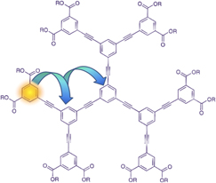
Light harvesting in dendrimer materials: Designer photophysics and electrodynamics
-
- Journal:
- Journal of Materials Research / Volume 27 / Issue 4 / 28 February 2012
- Published online by Cambridge University Press:
- 25 January 2012, pp. 627-638
- Print publication:
- 28 February 2012
-
- Article
- Export citation
A combined dislocation–cohesive zone model for fracture in nanocrystalline materials
-
- Journal:
- Journal of Materials Research / Volume 27 / Issue 4 / 28 February 2012
- Published online by Cambridge University Press:
- 25 January 2012, pp. 694-700
- Print publication:
- 28 February 2012
-
- Article
- Export citation

Yttria-stabilized zirconia crystallization in Al2O3/YSZ multilayers
-
- Journal:
- Journal of Materials Research / Volume 27 / Issue 6 / 28 March 2012
- Published online by Cambridge University Press:
- 25 January 2012, pp. 939-943
- Print publication:
- 28 March 2012
-
- Article
- Export citation
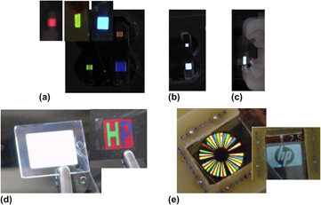
Development of semi-interpenetrating polymer networks and quantum dots–polymer nanocomposites for low-cost, flexible OLED display application
-
- Journal:
- Journal of Materials Research / Volume 27 / Issue 4 / 28 February 2012
- Published online by Cambridge University Press:
- 25 January 2012, pp. 639-652
- Print publication:
- 28 February 2012
-
- Article
- Export citation

Excitation spectrum of point defects in semiconductors studied by time-dependent density functional theory
-
- Journal:
- Journal of Materials Research / Volume 27 / Issue 6 / 28 March 2012
- Published online by Cambridge University Press:
- 24 January 2012, pp. 897-909
- Print publication:
- 28 March 2012
-
- Article
- Export citation
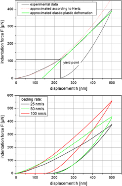
Measurement of the micromechanical properties of nanostructured aggregates via nanoindentation
-
- Journal:
- Journal of Materials Research / Volume 27 / Issue 4 / 28 February 2012
- Published online by Cambridge University Press:
- 23 January 2012, pp. 672-684
- Print publication:
- 28 February 2012
-
- Article
- Export citation

Nanoscale structure of Ti1−xNbyO2 mixed-phase thin films: Distribution of crystal phase and dopants
-
- Journal:
- Journal of Materials Research / Volume 27 / Issue 6 / 28 March 2012
- Published online by Cambridge University Press:
- 23 January 2012, pp. 944-950
- Print publication:
- 28 March 2012
-
- Article
- Export citation

Microcapsule-based materials for electrophoretic displays
-
- Journal:
- Journal of Materials Research / Volume 27 / Issue 4 / 28 February 2012
- Published online by Cambridge University Press:
- 20 January 2012, pp. 653-662
- Print publication:
- 28 February 2012
-
- Article
- Export citation
