Refine search
Actions for selected content:
106129 results in Materials Science

Microcompression study of Al-Nb nanoscale multilayers
-
- Journal:
- Journal of Materials Research / Volume 27 / Issue 3 / 14 February 2012
- Published online by Cambridge University Press:
- 20 January 2012, pp. 592-598
- Print publication:
- 14 February 2012
-
- Article
- Export citation

Observation of filament formation process of Cu/HfO2/Pt ReRAM structure by hard x-ray photoelectron spectroscopy under bias operation
-
- Journal:
- Journal of Materials Research / Volume 27 / Issue 6 / 28 March 2012
- Published online by Cambridge University Press:
- 20 January 2012, pp. 869-878
- Print publication:
- 28 March 2012
-
- Article
- Export citation
Dielectric and electric field–induced pyroelectric behavior of (Pb0.87−0.07xBa0.10+0.07x)La0.02(Zr0.7Sn0.15Ti0.15)O3 ceramics – CORRIGENDUM
-
- Journal:
- Journal of Materials Research / Volume 27 / Issue 2 / 28 January 2012
- Published online by Cambridge University Press:
- 20 January 2012, p. 506
- Print publication:
- 28 January 2012
-
- Article
- Export citation
JMR volume 27 issue 2 Cover and Back matter
-
- Journal:
- Journal of Materials Research / Volume 27 / Issue 2 / 28 January 2012
- Published online by Cambridge University Press:
- 20 January 2012, pp. b1-b2
- Print publication:
- 28 January 2012
-
- Article
-
- You have access
- Export citation
JMR volume 27 issue 2 Cover and Front matter
-
- Journal:
- Journal of Materials Research / Volume 27 / Issue 2 / 28 January 2012
- Published online by Cambridge University Press:
- 20 January 2012, pp. f1-f5
- Print publication:
- 28 January 2012
-
- Article
-
- You have access
- Export citation

Tunable dielectric properties in Mn-doped LuFe2O4 system
-
- Journal:
- Journal of Materials Research / Volume 27 / Issue 6 / 28 March 2012
- Published online by Cambridge University Press:
- 20 January 2012, pp. 922-927
- Print publication:
- 28 March 2012
-
- Article
- Export citation
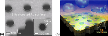
Atomic layer deposition: A versatile technique for plasmonics and nanobiotechnology
-
- Journal:
- Journal of Materials Research / Volume 27 / Issue 4 / 28 February 2012
- Published online by Cambridge University Press:
- 19 January 2012, pp. 663-671
- Print publication:
- 28 February 2012
-
- Article
- Export citation

Largely enhanced thermoelectric properties of the binary-phased PbTe–Sb2Te3 nanocomposites
-
- Journal:
- Journal of Materials Research / Volume 27 / Issue 4 / 28 February 2012
- Published online by Cambridge University Press:
- 19 January 2012, pp. 734-739
- Print publication:
- 28 February 2012
-
- Article
- Export citation

Application of clickable nanoporous silica surface for immobilization of ionic liquids
-
- Journal:
- Journal of Materials Research / Volume 27 / Issue 6 / 28 March 2012
- Published online by Cambridge University Press:
- 16 January 2012, pp. 932-938
- Print publication:
- 28 March 2012
-
- Article
- Export citation

A review of monolithic and multilayer coatings within the boron–carbon–nitrogen system by ion-beam-assisted deposition
-
- Journal:
- Journal of Materials Research / Volume 27 / Issue 5 / 14 March 2012
- Published online by Cambridge University Press:
- 16 January 2012, pp. 743-764
- Print publication:
- 14 March 2012
-
- Article
- Export citation

Surface irradiation and materials processing using polyatomic cluster ion beams
-
- Journal:
- Journal of Materials Research / Volume 27 / Issue 5 / 14 March 2012
- Published online by Cambridge University Press:
- 12 January 2012, pp. 806-821
- Print publication:
- 14 March 2012
-
- Article
- Export citation

Microstructure and compression behavior of chip consolidated magnesium
-
- Journal:
- Journal of Materials Research / Volume 27 / Issue 4 / 28 February 2012
- Published online by Cambridge University Press:
- 12 January 2012, pp. 709-719
- Print publication:
- 28 February 2012
-
- Article
- Export citation

Microwave dielectric properties of low loss and highly tunable Ba0.5Sr0.5Ti1−3y/2WyO3 ceramics
-
- Journal:
- Journal of Materials Research / Volume 27 / Issue 6 / 28 March 2012
- Published online by Cambridge University Press:
- 12 January 2012, pp. 910-914
- Print publication:
- 28 March 2012
-
- Article
- Export citation

Synthesis and characterization of germanium-centered three-dimensional crystalline porous aromatic framework
-
- Journal:
- Journal of Materials Research / Volume 27 / Issue 10 / 28 May 2012
- Published online by Cambridge University Press:
- 09 January 2012, pp. 1417-1420
- Print publication:
- 28 May 2012
-
- Article
- Export citation

Dominant shear bands observed in amorphous ZrCuAl nanowires under simulated compression
-
- Journal:
- MRS Communications / Volume 2 / Issue 1 / March 2012
- Published online by Cambridge University Press:
- 09 January 2012, pp. 13-16
- Print publication:
- March 2012
-
- Article
- Export citation

The Williams Dictionary of Biomaterials
-
- Published by:
- Liverpool University Press
- Published online:
- 05 January 2012
- Print publication:
- 27 May 1999
-
- Book
- Export citation
JMR volume 27 issue 1 Cover and Back matter
-
- Journal:
- Journal of Materials Research / Volume 27 / Issue 1 / 14 January 2012
- Published online by Cambridge University Press:
- 05 January 2012, pp. b1-b4
- Print publication:
- 14 January 2012
-
- Article
-
- You have access
- Export citation

Plastic response of the native oxide on Cr and Al thin films from in situ conductive nanoindentation
-
- Journal:
- Journal of Materials Research / Volume 27 / Issue 4 / 28 February 2012
- Published online by Cambridge University Press:
- 05 January 2012, pp. 685-693
- Print publication:
- 28 February 2012
-
- Article
- Export citation

Simple synthesis of polyaniline microtubes for the application on silver microrods preparation
-
- Journal:
- Journal of Materials Research / Volume 27 / Issue 2 / 28 January 2012
- Published online by Cambridge University Press:
- 05 January 2012, pp. 457-462
- Print publication:
- 28 January 2012
-
- Article
- Export citation
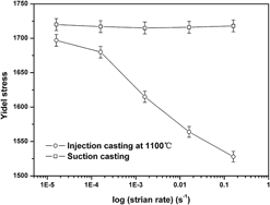
Correlation between strain-rate-related mechanical properties of Zr-based metallic glass and casting temperature
-
- Journal:
- Journal of Materials Research / Volume 27 / Issue 4 / 28 February 2012
- Published online by Cambridge University Press:
- 05 January 2012, pp. 701-708
- Print publication:
- 28 February 2012
-
- Article
- Export citation
