Refine search
Actions for selected content:
106116 results in Materials Science
Powder X-ray diffraction of bendamustine hydrochloride monohydrate, C16H22Cl2N3O2Cl·H2O
-
- Journal:
- Powder Diffraction / Volume 34 / Issue 1 / March 2019
- Published online by Cambridge University Press:
- 27 December 2018, pp. 74-75
-
- Article
- Export citation

Correlation between strain-rate sensitivity and viscous properties derived from dynamic nanoindentation of ultrafine-grained Al–Zn alloys
-
- Journal:
- MRS Communications / Volume 9 / Issue 1 / March 2019
- Published online by Cambridge University Press:
- 18 December 2018, pp. 310-314
- Print publication:
- March 2019
-
- Article
- Export citation
JMR volume 33 issue 23 Cover and Back matter
-
- Journal:
- Journal of Materials Research / Volume 33 / Issue 23 / 14 December 2018
- Published online by Cambridge University Press:
- 14 December 2018, pp. b1-b3
- Print publication:
- 14 December 2018
-
- Article
-
- You have access
- Export citation
JMR volume 33 issue 23 Cover and Front matter
-
- Journal:
- Journal of Materials Research / Volume 33 / Issue 23 / 14 December 2018
- Published online by Cambridge University Press:
- 14 December 2018, pp. f1-f6
- Print publication:
- 14 December 2018
-
- Article
-
- You have access
- Export citation
Crystal structures of ammonium citrates
-
- Journal:
- Powder Diffraction / Volume 34 / Issue 1 / March 2019
- Published online by Cambridge University Press:
- 11 December 2018, pp. 35-43
-
- Article
- Export citation
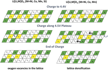
Si-doped high-energy Li1.2Mn0.54Ni0.13Co0.13O2 cathode with improved capacity for lithium-ion batteries
-
- Journal:
- Journal of Materials Research / Volume 33 / Issue 24 / 28 December 2018
- Published online by Cambridge University Press:
- 07 December 2018, pp. 4182-4191
- Print publication:
- 28 December 2018
-
- Article
- Export citation
Research Highlights: Perovskites
-
- Journal:
- MRS Bulletin / Volume 43 / Issue 12 / December 2018
- Published online by Cambridge University Press:
- 10 December 2018, pp. 909-910
- Print publication:
- December 2018
-
- Article
-
- You have access
- HTML
- Export citation
Hideo Hosono: 2018 Von Hippel Award winner and passionate materials scientist
-
- Journal:
- MRS Bulletin / Volume 43 / Issue 12 / December 2018
- Published online by Cambridge University Press:
- 10 December 2018, p. 980
- Print publication:
- December 2018
-
- Article
-
- You have access
- HTML
- Export citation

Crack propagation in porous polymer sheets with different pore sizes
-
- Journal:
- MRS Communications / Volume 8 / Issue 4 / December 2018
- Published online by Cambridge University Press:
- 18 December 2018, pp. 1477-1482
- Print publication:
- December 2018
-
- Article
-
- You have access
- Open access
- HTML
- Export citation
Automotive clearcoats characterized in search for improvement
-
- Journal:
- MRS Bulletin / Volume 43 / Issue 12 / December 2018
- Published online by Cambridge University Press:
- 10 December 2018, p. 911
- Print publication:
- December 2018
-
- Article
-
- You have access
- HTML
- Export citation
Improving the efficiency of concentrating solar power systems
-
- Journal:
- MRS Bulletin / Volume 43 / Issue 12 / December 2018
- Published online by Cambridge University Press:
- 10 December 2018, pp. 920-921
- Print publication:
- December 2018
-
- Article
-
- You have access
- HTML
- Export citation
MRS volume 43 issue 12 Cover and Front matter
-
- Journal:
- MRS Bulletin / Volume 43 / Issue 12 / December 2018
- Published online by Cambridge University Press:
- 10 December 2018, pp. f1-f6
- Print publication:
- December 2018
-
- Article
-
- You have access
- Export citation
Advanced magnetic materials could drive next-generation energy technologies
-
- Journal:
- MRS Bulletin / Volume 43 / Issue 12 / December 2018
- Published online by Cambridge University Press:
- 10 December 2018, pp. 918-919
- Print publication:
- December 2018
-
- Article
-
- You have access
- HTML
- Export citation
MRC volume 8 issue 4 Cover and Back matter
-
- Journal:
- MRS Communications / Volume 8 / Issue 4 / December 2018
- Published online by Cambridge University Press:
- 09 January 2019, pp. b1-b2
- Print publication:
- December 2018
-
- Article
-
- You have access
- Export citation
Optimizing thermal conduction in bulk polycrystalline SrTiO3−δ ceramics via oxygen non-stoichiometry – ERRATUM
-
- Journal:
- MRS Communications / Volume 8 / Issue 4 / December 2018
- Published online by Cambridge University Press:
- 09 January 2019, p. 1484
- Print publication:
- December 2018
-
- Article
-
- You have access
- HTML
- Export citation
Plastic waste is the last straw, says UK
-
- Journal:
- MRS Bulletin / Volume 43 / Issue 12 / December 2018
- Published online by Cambridge University Press:
- 10 December 2018, pp. 913-914
- Print publication:
- December 2018
-
- Article
-
- You have access
- HTML
- Export citation

Piezo-phototronic effect on optoelectronic nanodevices
-
- Journal:
- MRS Bulletin / Volume 43 / Issue 12 / December 2018
- Published online by Cambridge University Press:
- 10 December 2018, pp. 952-958
- Print publication:
- December 2018
-
- Article
- Export citation

Piezotronic materials and large-scale piezotronics array devices
-
- Journal:
- MRS Bulletin / Volume 43 / Issue 12 / December 2018
- Published online by Cambridge University Press:
- 10 December 2018, pp. 936-940
- Print publication:
- December 2018
-
- Article
- Export citation

Piezotronics and piezo-phototronics in two-dimensional materials
-
- Journal:
- MRS Bulletin / Volume 43 / Issue 12 / December 2018
- Published online by Cambridge University Press:
- 10 December 2018, pp. 959-964
- Print publication:
- December 2018
-
- Article
- Export citation

Piezotronic sensors
-
- Journal:
- MRS Bulletin / Volume 43 / Issue 12 / December 2018
- Published online by Cambridge University Press:
- 10 December 2018, pp. 941-945
- Print publication:
- December 2018
-
- Article
- Export citation
