Refine search
Actions for selected content:
106116 results in Materials Science
Amorphous Semiconductors: Structural, Optical, and Electronic Properties by Kazuo Morigaki, Sándor Kugler, and Koichi Shimakawa
-
- Journal:
- MRS Bulletin / Volume 43 / Issue 12 / December 2018
- Published online by Cambridge University Press:
- 10 December 2018, p. 981
- Print publication:
- December 2018
-
- Article
-
- You have access
- HTML
- Export citation
Dendrimer templates enable growth of multimetallic sub-nanoclusters
-
- Journal:
- MRS Bulletin / Volume 43 / Issue 12 / December 2018
- Published online by Cambridge University Press:
- 10 December 2018, p. 912
- Print publication:
- December 2018
-
- Article
-
- You have access
- HTML
- Export citation
Raw materials use to double by 2060 with severe environmental consequences
-
- Journal:
- MRS Bulletin / Volume 43 / Issue 12 / December 2018
- Published online by Cambridge University Press:
- 10 December 2018, p. 914
- Print publication:
- December 2018
-
- Article
-
- You have access
- HTML
- Export citation

Piezophotonics: From fundamentals and materials to applications
-
- Journal:
- MRS Bulletin / Volume 43 / Issue 12 / December 2018
- Published online by Cambridge University Press:
- 10 December 2018, pp. 965-969
- Print publication:
- December 2018
-
- Article
- Export citation
Using the near-absolute-zero temperature of outer space to cool things on Earth
-
- Journal:
- MRS Bulletin / Volume 43 / Issue 12 / December 2018
- Published online by Cambridge University Press:
- 10 December 2018, pp. 915-917
- Print publication:
- December 2018
-
- Article
-
- You have access
- HTML
- Export citation
Separating photo-induced electrons provides a new paradigm in optoelectronic control
-
- Journal:
- MRS Bulletin / Volume 43 / Issue 12 / December 2018
- Published online by Cambridge University Press:
- 10 December 2018, pp. 910-911
- Print publication:
- December 2018
-
- Article
-
- You have access
- HTML
- Export citation
MRC volume 8 issue 4 Cover and Front matter
-
- Journal:
- MRS Communications / Volume 8 / Issue 4 / December 2018
- Published online by Cambridge University Press:
- 09 January 2019, pp. f1-f5
- Print publication:
- December 2018
-
- Article
-
- You have access
- Export citation

Piezotronics and piezo-phototronics with third-generation semiconductors
-
- Journal:
- MRS Bulletin / Volume 43 / Issue 12 / December 2018
- Published online by Cambridge University Press:
- 10 December 2018, pp. 922-927
- Print publication:
- December 2018
-
- Article
-
- You have access
- HTML
- Export citation
LOOK AGAIN
-
- Journal:
- MRS Bulletin / Volume 43 / Issue 12 / December 2018
- Published online by Cambridge University Press:
- 10 December 2018, p. 984
- Print publication:
- December 2018
-
- Article
-
- You have access
- HTML
- Export citation

Theory of piezotronics and piezo-phototronics
-
- Journal:
- MRS Bulletin / Volume 43 / Issue 12 / December 2018
- Published online by Cambridge University Press:
- 10 December 2018, pp. 928-935
- Print publication:
- December 2018
-
- Article
- Export citation
Graphene: Fabrication, Characterizations, Properties and Applications by Hongwei Zhu, Zhiping Xu, Dan Xie, and Ying Fang, Editors
-
- Journal:
- MRS Bulletin / Volume 43 / Issue 12 / December 2018
- Published online by Cambridge University Press:
- 10 December 2018, p. 982
- Print publication:
- December 2018
-
- Article
-
- You have access
- HTML
- Export citation
CAREER CENTRAL
-
- Journal:
- MRS Bulletin / Volume 43 / Issue 12 / December 2018
- Published online by Cambridge University Press:
- 10 December 2018, p. 983
- Print publication:
- December 2018
-
- Article
-
- You have access
- Export citation
Piezotronic modulations in electro- and photochemical catalysis
-
- Journal:
- MRS Bulletin / Volume 43 / Issue 12 / December 2018
- Published online by Cambridge University Press:
- 10 December 2018, pp. 946-951
- Print publication:
- December 2018
-
- Article
- Export citation
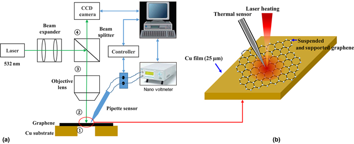
Characterization of interface thermal resistance between graphene and Cu film by using a micropipette thermography technique
-
- Journal:
- MRS Communications / Volume 8 / Issue 4 / December 2018
- Published online by Cambridge University Press:
- 03 December 2018, pp. 1463-1469
- Print publication:
- December 2018
-
- Article
- Export citation
Elements of Structures and Defects of Crystalline Materials by Tsang-Tse Fang
-
- Journal:
- MRS Bulletin / Volume 43 / Issue 12 / December 2018
- Published online by Cambridge University Press:
- 10 December 2018, pp. 981-982
- Print publication:
- December 2018
-
- Article
-
- You have access
- HTML
- Export citation
In memoriam: Julia Weertman (1926–2018) and Johannes Weertman (1925–2018)
-
- Journal:
- MRS Bulletin / Volume 43 / Issue 12 / December 2018
- Published online by Cambridge University Press:
- 10 December 2018, pp. 978-979
- Print publication:
- December 2018
-
- Article
-
- You have access
- HTML
- Export citation
MRS volume 43 issue 12 Cover and Back matter
-
- Journal:
- MRS Bulletin / Volume 43 / Issue 12 / December 2018
- Published online by Cambridge University Press:
- 10 December 2018, pp. b1-b2
- Print publication:
- December 2018
-
- Article
-
- You have access
- Export citation

Voltage-controlled magnetoelectric memory and logic devices
-
- Journal:
- MRS Bulletin / Volume 43 / Issue 12 / December 2018
- Published online by Cambridge University Press:
- 10 December 2018, pp. 970-977
- Print publication:
- December 2018
-
- Article
- Export citation
Perspectives on frontiers in electronic and photonic materials
-
- Journal:
- MRS Bulletin / Volume 43 / Issue 12 / December 2018
- Published online by Cambridge University Press:
- 10 December 2018, pp. 901-908
- Print publication:
- December 2018
-
- Article
-
- You have access
- HTML
- Export citation
JMR volume 33 issue 22 Cover and Front matter
-
- Journal:
- Journal of Materials Research / Volume 33 / Issue 22 / 28 November 2018
- Published online by Cambridge University Press:
- 28 November 2018, pp. f1-f5
- Print publication:
- 28 November 2018
-
- Article
-
- You have access
- Export citation
