To save content items to your account,
please confirm that you agree to abide by our usage policies.
If this is the first time you use this feature, you will be asked to authorise Cambridge Core to connect with your account.
Find out more about saving content to .
To save content items to your Kindle, first ensure no-reply@cambridge.org
is added to your Approved Personal Document E-mail List under your Personal Document Settings
on the Manage Your Content and Devices page of your Amazon account. Then enter the ‘name’ part
of your Kindle email address below.
Find out more about saving to your Kindle.
Note you can select to save to either the @free.kindle.com or @kindle.com variations.
‘@free.kindle.com’ emails are free but can only be saved to your device when it is connected to wi-fi.
‘@kindle.com’ emails can be delivered even when you are not connected to wi-fi, but note that service fees apply.
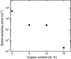
Copper/diamond-like carbon (DLC) was fabricated using pulsed laser deposition, and the effects of copper on the properties of DLC composites were studied. Experimental results showed that the presence of copper promoted surface evolution through the formation of nanoclusters, accentuated the formation of Si–C but graphitized the diamond bondings of DLC matrix. By considering the interaction of laser with copper/carbon composite target, the presence of copper may have increased the energy absorbed during laser deposition, as envisaged by Saha’s equation. Thus, upon the impingement of ions on substrate during deposition, the carbon and silicon atoms may have been redistributed to form Si–C bonding while the excess energy was released as heat to promote the formation of nanoclusters but graphitize the sp3 bonding in DLC. Although sp3 bonding was reduced with the presence of copper, mechanical characterization showed that the adhesion strength of the composite films was approximately five times higher compared to undoped DLC, as a result of the decrease in internal stress and the formation of Si–C bondings in DLC.
Using in situ indentation, we show that highly localized and well-defined mechanical deformation can be coupled with structural and electronic characterization in the scanning tunneling microscope. Dislocations induced in Ni(100) were topographically imaged and probed by scanning tunneling spectroscopy to assess their effect on local surface electronic structure. Compared with undamaged terraces, dislocation regions exhibited a significant increase in local density of states near the Fermi level, and enhanced reactivity toward oxidation. In the context of the d-band electronic structure model, we suggest that the undercoordination of atoms and residual strain resulting from plastic deformation serve to locally accelerate adsorption-driven chemical reactions with species such as molecular oxygen.
This article investigates the effect of grain structure on electromigration (EM) reliability of dual-damascene Cu interconnects with a CoWP capping layer, including the lifetime and statistics. Downstream EM tests were performed on two sets of CoWP-capped Cu interconnects with different grain sizes. Compared to Cu interconnects with the standard SiCN cap layer, the CoWP capping clearly improved the EM lifetime by ∼24× for the small grain structure and by another ∼14× for the large grain structure. Here, the effect of grain structure on EM lifetime was attributed to the grain boundary contribution to mass transport. The lifetime improvement, however, was accompanied with an increase in the statistical deviation, increasing from 0.27 for the SiCN cap to 0.53 for the small grain structure and to 0.88 for the large grain structure with the CoWP cap. This was attributed to the effect of grain structure in changing the statistical distribution of flux divergence sites and thus the failure statistics.
Conventionally, mean grain size is considered the most critical microstructural parameter in determining the mechanical behavior of pure metals. By systematically controlling the distribution of grain orientations in aluminum films, we show that microstructural heterogeneity alone induces large variation in the mechanical behavior of nanocrystalline metal films. Aluminum films with relatively homogeneous microstructure (all grains with identical out-of-plane orientation) show substantially less early Bauschinger effect compared to films with heterogeneous microstructure, irrespective of film thickness or grain size. On the other hand, the films with homogeneous microstructure show relatively higher yield stresses. A direct correspondence is found between the nonuniformity of plastic deformation and early Bauschinger effect, which confirms the critical role of microstructural heterogeneity.
Expanded graphite/cobalt ferrite/polyaniline (EG/CF/PANI) ternary composites were obtained by a two-step process. The intercalation compound, CF embedded in EG, was synthesized by a coprecipitation method. PANI could then be coated on the surface of the EG/CF microparticles by in-situ polymerization to form ternary composites of EG/CF/PANI. The results indicate that the electrical and magnetic performance of EG/CF and EG/CF/PANI composites are related to their composition. The EG/CF composite with mass ratio of 1.0 has the maximal conductivity (833.33 S·cm−1) among the binary composites. Saturation magnetizations (Ms) of the EG/CF composite with mEG/mCF of 0.8 is the largest among EG/CF composites, the ternary composites of EG/CF/PANI were prepared from the EG/CF composite at this mass ratio. The electromagnetic wave absorbing property of all ternary composites excelled those of EG/CF composites, and the sample with 40 wt% of PANI has the best absorption properties in the range of 8–18 GHz frequency.
Single-crystal silicon test specimens, fabricated by lithography and deep reactive ion etching (DRIE), were used to measure microscale deformation and fracture properties. The mechanical properties of two specimen geometries, both in the form of a Greek letter Θ (theta), were measured using an instrumented indentation system. The DRIE process generated two different surface structures leading to two strength distributions that were specimen geometry independent: One distribution, centered about 2.1 GPa, was controlled by 35 nm surface roughness of scallops; the second distribution, centered about 1.4 GPa, was controlled by larger, 150 nm, pitting defects. Finite element analyses (FEA) converted measured loads into strengths; tensile elastic measurements validated the FEA. Fractographic observations verified failure locations. The theta specimen and testing protocols are shown to be extremely effective at testing statistically relevant (hundreds) numbers of samples to establish processing–structure–property relationships at ultrasmall scales and for determining design parameters for components of microelectromechanical systems.
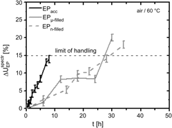
Epoxy–dicyandiamide (Dicy) formulations frequently contain a free accelerator for reducing the curing temperature and the time for network formation, which reduces the shelf life of these adhesives. This study compared the reaction kinetics during the storage at 60 °C for a precured epoxy adhesive (EP = diglycidyl ether of bisphenol A and Dicy, mass ratio 100:6.7, precured at 150 °C for 1 h) mixed either with free accelerator (=EPacc) or with the same concentration of accelerator immobilized in micro- or nanozeolite fillers (EPμ-filled and EPn-filled, respectively). During storage, the infrared (IR) study probed the chemical modifications. They lead to increasing cross-linking density and a loss of free volume as detected by positron annihilation lifetime spectroscopy (PALS). Cross-linking precedes to the chemical vitrification. Additionally, the glass transition and the free-volume parameters were investigated for the three EP’s as a function of temperature by PALS after thermal curing.
This study confirms the existence of several nanometer-ordered structures in amorphous Al2O3–2SiO2–Na2O–7H2O geopolymers by high-resolution transmission electron microscopy and selected area electron diffraction. The composition ratio of the geopolymers was designed according to the NaA zeolite composition (Si/Al/Na atom ratio of 1:1:1), and the expected NaA molecular sieve was achieved by the Al2O3–2SiO2–Na2O–7H2O geopolymers through a hydrothermal reaction. This design concept was used to convert geopolymers into zeolite molecular sieves and provides a new preparation method for zeolite membranes or zeolite bulk materials.
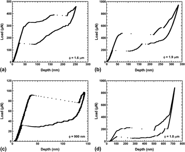
Shape memory alloys (SMA) undergo reversible martensitic transformation in response to changes in temperature or applied stress, resulting in the properties of superelasticity and shape memory. At present, there is high scientific and technological interest to develop these properties at small scales and apply SMA as sensors and actuators in microelectromechanical system technologies. To study the thermomechanical properties of SMA at micro and nanoscales, instrumented nanoindentation is widely used to conduct nanopillar compression tests. By using this technique, superelasticity and shape memory at the nanoscale have been demonstrated in micro and nanopillars of Cu–Al–Ni SMA. However, the martensitic transformation seems to exhibit different behavior at small scales, and a size effect on superelasticity has been recently reported. In this study, we provide an overview of the thermomechanical properties of Cu–Al–Ni SMA at the nanoscale, with special emphasis on size effects. Finally, these size effects are discussed in light of the microscopic mechanisms controlling the martensitic transformation at the nanoscale.
We analyzed the contact mechanisms of bioinspired microfibrillar adhesives using in situ scanning electron microscopy. During adhesion tests we observed that (i) the superior adhesion of mushroom-shaped fibrils is assisted by the stochastic nature of detachment, (ii) the aspect ratio of microfibrils influences the bending/buckling behavior and the contact reformation, and (iii) the backing layer deformation causes the microfibrils to elastically interact with each other. These studies give new insights into the mechanisms responsible for adhesion of bioinspired fibrillar adhesives.
Al/SiC nanolaminates have been shown to possess excellent combination of mechanical strength and flexibility. While metal–ceramic multilayers present a tremendous opportunity for hard coatings, the strength evaluation is usually carried out under static loading conditions such as nanoindentation and microcompression testing. In this study, we have studied the scratch resistance behavior of Al/SiC nanolaminates. These properties are then compared to monolithic films of Al and SiC. Finally, the deformation behavior under such loading was quantified by critical load, work of deformation, and postexperimental microstructural analysis by scanning electron microscopy and focused ion beam cross sections. It is shown that the combination of hard SiC and plastic Al layers provides enhanced resistance to scratch loading and makes these materials as very good candidates for wear-resistant coatings.
A self-taught authority on electromagnetic theory, telegraphy and telephony, Oliver Heaviside (1850–1925) dedicated his adult life to the improvement of electrical technologies. Inspired by James Clerk Maxwell's field theory, he spent the 1880s presenting his ideas as a regular contributor to the weekly journal, The Electrician. The publication of Electrical Papers, a year after his election to the Royal Society in 1891, established his fame beyond the scientific community. An eccentric figure with an impish sense of humour, Heaviside's accessible style enabled him to educate an entire generation in the importance and application of electricity. In so doing he helped to establish that very British phenomenon, the garden-shed inventor. Illustrated with practical examples, the subjects covered in Volume 1 include voltaic constants, duplex telegraphy, microphones and electromagnets.
Bamboo is a typical natural fiber-reinforced composite material with superior mechanical properties. As the reinforce phase in bamboo composite, the vascular bundles were extracted from different height locations of a Moso bamboo with an alkali treatment method, and the mechanical properties were investigated via the tensile test. It is found that both the longitudinal Young’s modulus and strength of the vascular bundles are linearly increased from the inner to outer side. To study the variation of mechanical properties of bamboo culm along the radial direction, thin bamboo slices were also tested. Using a modified rule of mixtures, the longitudinal Young’s modulus of bamboo slices are analyzed and excellent agreement can be found between experimental and theoretical results, which indicates that the longitudinal Young’s modulus of bamboo culm is cubically increased in the radial direction.
The current work describes the simple solution process of ball-chain polycrystalline Fe nanofibers with aspect ratios (λ) and diameters (D) of over 1−65 and 30−95 nm. Static magnetic and microwave electromagnetic property studies demonstrated that such properties strongly depend on the λ and D of the Fe nanofibers. As the λ and D increase, the U-shape of the saturation magnetization (Ms) reaches a maximum of 180.0 emu·g−1, owing to the cooperative action of nanoeffects and magnetic interactions, whereas the coercivity (Hc) gradually increases due to aspect ratio variations. In contrast, the change in trends of the permittivity (ε′, ε″) and the dielectric loss (tgδE) are represented as an inverted U-shape; the permeability (μ′, μ″) and magnetic loss (tgδM) increase at low-frequency ranges and decrease at high frequency ranges. Stronger absorption and broader bandwidths of Fe nanofibers compared with Fe nanoparticles are ascribed to higher dielectric losses. The prepared Fe nanofibers have high potential in light-weight and broad bandwidth microwave absorbing applications.
The direct integration of Ge nanowires with silicon is of interest in multiple applications. In this work, we describe the growth of high-quality, vertically oriented Ge nanowires on Si (111) substrates utilizing a completely sub-Au–Si-eutectic annealing and growth procedure. With all other conditions remaining identical, annealing below the Au–Si eutectic results in successful heteroepitaxial nucleation and growth of Ge nanowires on Si substrate while annealing above the Au–Si eutectic leads to randomly oriented growth. A model is presented to elucidate the effect of the annealing temperature, in which we hypothesized that sub-Au–Si-eutectic annealing leads to the formation of a single and well-oriented interface, essential to template heteroepitaxial nucleation. These results are critically dependent on substrate preparation and lead to the creation of integrated nanowire systems with a low thermal budget process.