To save content items to your account,
please confirm that you agree to abide by our usage policies.
If this is the first time you use this feature, you will be asked to authorise Cambridge Core to connect with your account.
Find out more about saving content to .
To save content items to your Kindle, first ensure no-reply@cambridge.org
is added to your Approved Personal Document E-mail List under your Personal Document Settings
on the Manage Your Content and Devices page of your Amazon account. Then enter the ‘name’ part
of your Kindle email address below.
Find out more about saving to your Kindle.
Note you can select to save to either the @free.kindle.com or @kindle.com variations.
‘@free.kindle.com’ emails are free but can only be saved to your device when it is connected to wi-fi.
‘@kindle.com’ emails can be delivered even when you are not connected to wi-fi, but note that service fees apply.
As plasmonic materials transition from three-dimensional to two-dimensional (2D) form, unique optical and electronic phenomena arise that are unattainable in bulk materials and conventional thin films. Exceptional sensitivity to external perturbations, including electrical biasing and optical excitation as well as quantum effects, are expected to emerge, as has been demonstrated in graphene. Similarly, metallic or plasmonic films with thicknesses down to a few monolayers, called transdimensional materials (TDMs), are predicted to exhibit remarkably strong tunability of their optical response. The unique properties of 2D materials and TDMs have established them as promising platforms for dynamic nanophotonic devices. While novel 2D materials have been widely explored for nanophotonic devices, until recently, there have been minimal studies on the evolution of the optical properties of plasmonic TDMs. In this article, we highlight progress in exploring the thickness-dependent optical response of plasmonic materials as they approach the 2D regime. Experimental and theoretical investigations of the plasmonic properties of 2D materials, such as graphene and tungsten diselenide, TDMs, and plasmonic thin films, are discussed, with a focus on prospects for their utilization in dynamically tunable flat optical devices or metasurfaces.
This article presents a brief review of our case studies of data-driven Integrated Computational Materials Engineering (ICME) for intelligently discovering advanced structural metal materials, including light-weight materials (Ti, Mg, and Al alloys), refractory high-entropy alloys, and superalloys. The basic bonding in terms of topology and electronic structures is recommended to be considered as the building blocks/units constructing the microstructures of advanced materials. It is highlighted that the bonding charge density could not only provide an atomic and electronic insight into the physical nature of chemical bond of materials but also reveal the fundamental strengthening/embrittlement mechanisms and the local phase transformations of planar defects, paving a path in accelerating the development of advanced metal materials via interfacial engineering. Perspectives on the knowledge-based modeling/simulations, machine-learning knowledge base, platform, and next-generation workforce for sustainable ecosystem of ICME are highlighted, thus to call for more duty on the developments of advanced structural metal materials and enhancement of research productivity and collaboration.
The effects of stress-free and stress-assisted pretreatments at a relatively high temperature on the creep properties of [001] and [011] oriented Ni-based single-crystal superalloys are investigated in this article. The results show that the creep life of the pretreated samples is shorter than that of the original samples. The variation of the γ/γ′ morphology during the creep process is characterized by the microstructure period. Based on the interaction between the dislocations in the γ matrix channel and the γ′ phase, the difference in creep properties of the two oriented alloys after pretreatment is analyzed. Combined with the crystal plasticity theory and the number of activated slip systems observed in the experiments, it can be concluded that the two oriented alloys after pretreatment show obvious creep anisotropy and that the creep life increases with the number of activated slip system.
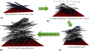
To avoid degradation of silicon anodes in lithium-ion batteries (LIBs), the authors report a new two-dimensional multi-layered Si-intercalated rGO (rGO/Si) anode prepared by direct growth of Si into a porous multi-layered reduced graphene oxide (rGO) film. Direct Si deposition onto the porous rGO film allows the Si layers to be intercalated into the film via in situ replacement of the oxygen groups of the multi-layered graphene oxide (GO) with Si through thermal reduction of the GO film. The porous rGO acts as a cushion against the expansion of the Si layer during lithiation, preventing the Si from being pulverized and producing highly stable LIBs.
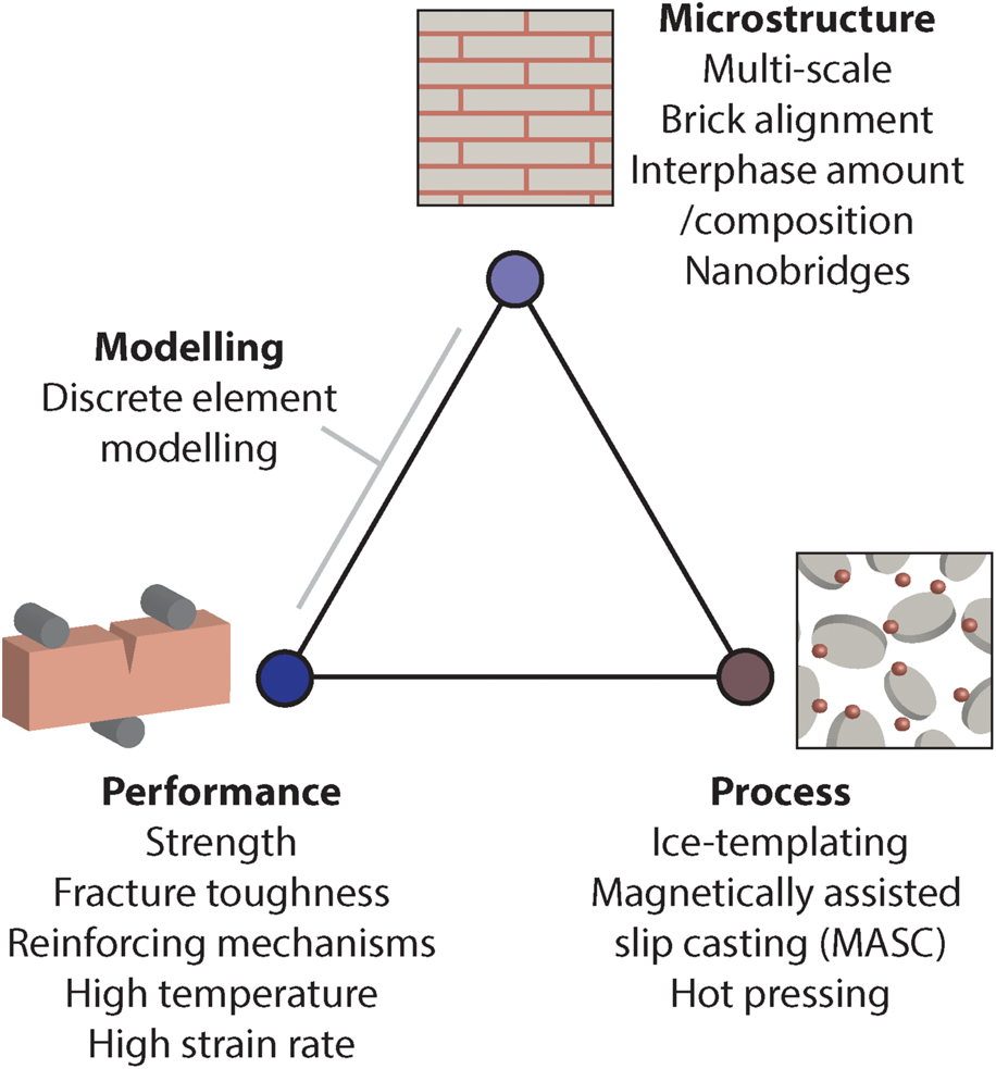
The materials chosen to make thermal engines, spacecrafts, or human implants cannot fail in an unpredictable way to guarantee the users' well-being. These applications can benefit from the use of ceramics because of their temperature resistance, corrosion resistance, or hardness. Although parts based on ceramic matrix composites and zirconia are already in use, a more recent ceramic with a structure inspired from seashells provides an attractive combination of ease of processing, high strength, and high toughness. These nacre-like aluminas are made of aligned micron-sized monocrystalline platelets joined together by a mix of mineral secondary phase and nanoparticles. The review's first objective is to provide a picture of what these newly developed bioinspired ceramics are capable of within today's ceramic and nacre-inspired composites landscape. I will also extract from the results the links between process/microstructure/performance to better understand the potential of these materials in terms of toughness and strength increase. Finally, I will present the challenges that are ahead to eventually reproduce the exceptional fracture behavior observed in nacre.
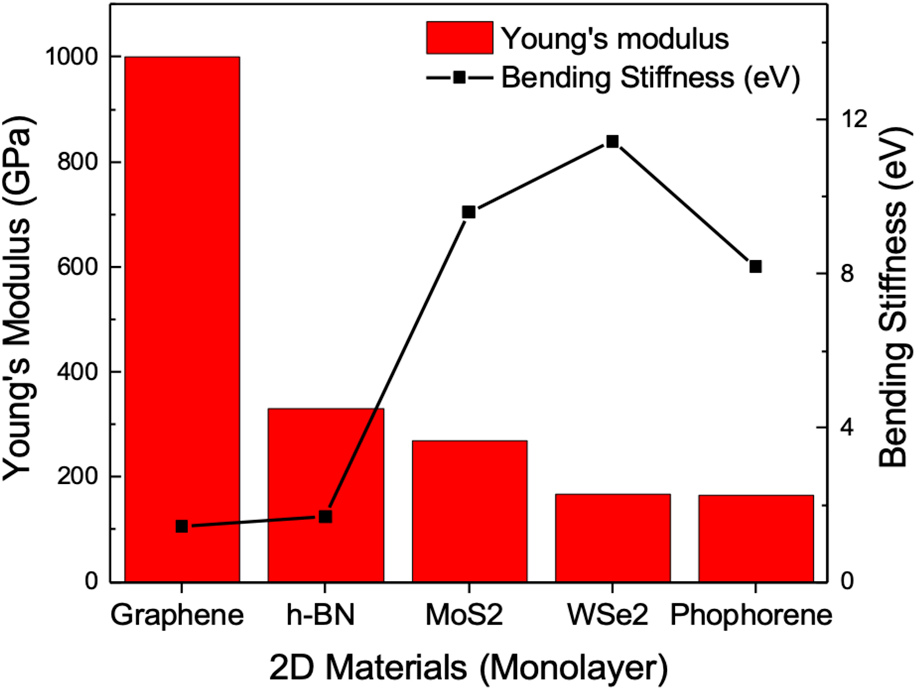
Atomically thin 2D materials exhibit strong intralayer covalent bonding and weak interlayer van der Waals interactions, offering unique high in-plane strength and out-of-plane flexibility. While atom-thick nature of 2D materials may cause uncontrolled intrinsic/extrinsic deformation in multiple length scales, it also provides new opportunities for exploring coupling between heterogeneous deformations and emerging functionalities in controllable and scalable ways for electronic, optical, and optoelectronic applications. In this review, we discuss (i) the mechanical characteristics of 2D materials, (ii) uncontrolled inherent deformation and extrinsic heterogeneity present in 2D materials, (iii) experimental strategies for controlled heterogeneous deformation of 2D materials, (iv) 3D structure-induced novel functionalities via crumple/wrinkle structure or kirigami structures, and (v) heterogeneous strain-induced emerging functionalities in exciton and phase engineering. Overall, heterogeneous deformation offers unique advantages for 2D materials research by enabling spatial tunability of 2D materials' interactions with photons, electrons, and molecules in a programmable and controlled manner.
Recently, layered double hydroxides (LDHs) have attracted intensive research interest as the next-generation supercapacitor electrodes due to their unique two-dimensional (2D) hydrotalcite-like structure. However, the inevitable agglomeration significantly decreases the accessible surface areas and blocks the pseudocapacitive sites, thus severely hinders their electrochemical applications. Herein, we develop a facile one-step growth approach to fabricate porous agglomerate of NiCo-LDH nanosheets and reduced graphene oxide (rGO) nanoflakes. By adjusting feeding molar ratios, the obtained NiCo-LDH/rGO electrode delivers a high specific capacity of 879.5 C/g at a current density of 0.5 A/g and still remains 485 C/g at 20 A/g. Furthermore, the fabricated asymmetric supercapacitor (ASC) has demonstrated a superior energy density of 48.7 W h/kg at a power density of 401 W/kg. After 2000 cycles, the assembled ASC exhibits an improved capacity retention of 81% within a potential window of 1.6 V at 2 A/g.
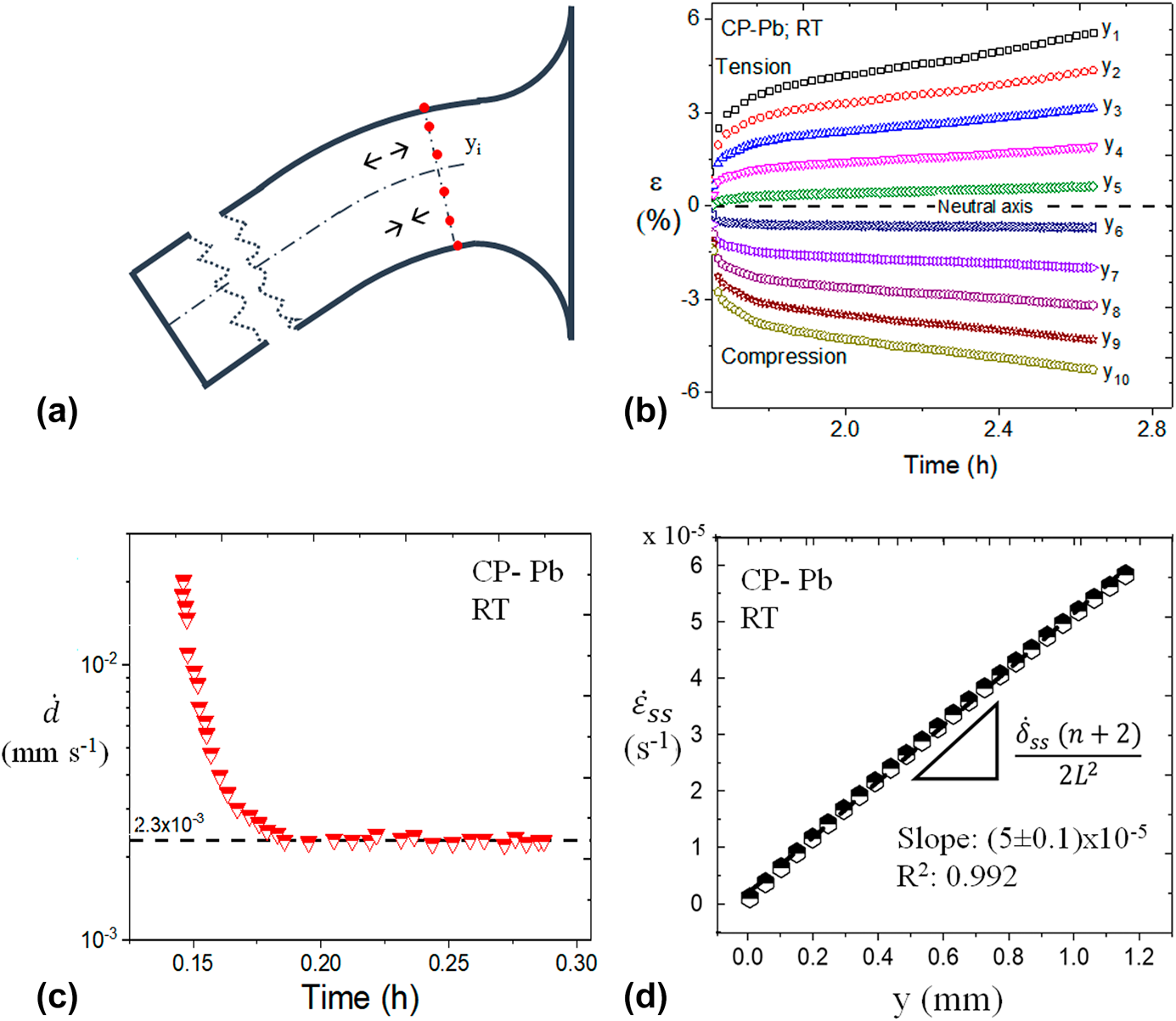
Variation of stress across the length and thickness of a cantilever during creep allows obtaining multiple pairs of strain rates and stress under steady-state condition. This work applies digital image correlation (DIC) and conjugate analytical models to obtain several such “strain rate–stress” pairs during steady-state creep by testing a single cantilever at a constant applied load. Furthermore, these strain rate–stress pairs are used to accurately determine the stress exponent of the material (e.g., Al and Pb). In addition, an empirical observation of plotting strain rate as a function of stress at fixed strain during primary creep for estimating stress exponent is extended to bending creep, wherein strain rates of the points in the cantilever lying on an iso-strain contour were plotted against the moment at the point to determine stress exponent. This study, thereby, proves that the “bending creep–DIC” combination is a high throughput test methodology for studying steady-state creep.
The stress and hence strain fields in a cantilever deforming as per power-law creep vary across the length and thickness of the sample, which allow obtaining multiple stress–strain pairs from a single test. Here, a high-throughput method is described to quantify the primary-cum-steady-state creep response of materials by testing a single cantilever sample in bending and mapping strain fields using digital image correlation. The method is based on the existence of stress invariant points in a cantilever, where the value of stress does not change during creep. It is demonstrated that strain evolution throughout primary and steady-state stages at these points is identical to the creep response obtained under uniaxial tests. Furthermore, the gained insights were exploited to obtain various parameters of a power-law type primary-cum-steady-state creep equation by testing only one cantilever sample. The developed method allows obtaining uniaxial creep curves at multiple stresses by testing a single cantilever, thereby reducing the time and number of samples required to understand the creep behavior of a material. The method has been validated by performing bending tests on Al and comparing the results with those of corresponding uniaxial tests.
With the ever-increasing importance of nanoscale deformation phenomena in contemporary technologies, basic understanding of material behavior at the nanoscale has become of critical importance. Especially, nanomechanical testing that provides the capability to study fundamental nanoscale deformation and phase change phenomena in real time and under controlled loading conditions is essential for nanomaterial research. In this study, acoustic emission (AE) was used in situ to characterize nanoindentation-induced deformation, microfracture, and phase transformation processes intrinsic of bulk single-crystal MgO and polycrystalline Al, thin films of polycrystalline SiC, and thick films of austenitic TiNi shape-memory alloy. Scale-dependent plastic deformation and microfracture affected by the indenter tip radius and the applied normal load are interpreted in terms of the type and intensity of AE events revealed by abrupt displacement excursions in the loading response of the indented materials. The amplitudes of AE waveforms are used to examine characteristic deformation, microfracture, and phase change mechanisms in the time domain. Fast Fourier transformation and short-time Fourier transformation analyses provide further insight into the material behavior and structural changes due to indentation loading in the frequency and time-frequency domain, respectively. The methodology developed in this study represents an effective approach for nanomechanical testing and in situ characterization of nanoscale deformation, microfracture, and phase transformation phenomena.
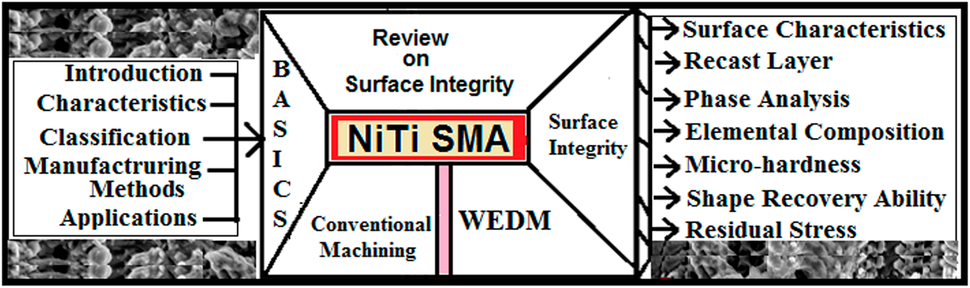
NiTi shape memory alloys (SMAs) are extensively used in various significant areas such as aerospace industries, biomedical sector, automobile industries, and robotics field because of their inherent properties, namely, shape memory effect and superelasticity. Nevertheless, the machining of these alloys is a problematic task by conventional machining practices because of various difficulties such as strain hardening, tool failure, high machining time, and poor surface quality. In recent years, researchers have explored various advanced/unconventional machining processes to surmount these challenges and improve the performance characteristics of NiTi SMAs. Wire electrical discharge machining (WEDM) is an effective and reasonable alternative to machine these hard-to-machine alloys among the other available advanced machining processes. A brief overview, characteristics, applications, and conventional machining of NiTi SMAs have been incorporated in this study. This review article provides substantial insight into the various aspects of surface integrity (SI) for NiTi SMAs using WEDM. The current study highlights literature review on the research work accomplished so far in the domain of SI aspects for NiTi-based SMAs, namely, surface characteristics, react layer, phase analysis, elemental composition, micro-hardness, shape recovery ability, and residual stress in WEDM.
Uranium–35 wt.% zirconium (U–35 wt.% Zr) alloy was annealed for 1 h and 24 h at 650 °C and characterized to understand the early-stage microstructure evolution. Dendritic microstructure with fine (∼300 nm in length) α-U precipitates clustered between dendrite branches were observed in the 1-h annealed sample. After 24-h annealing at 650 °C, the α-U precipitates coarsened, and the dendritic microstructure disappeared because of microstructure homogenization. Furthermore, microchemical homogenization observed with energy-dispersive X-ray spectroscopy analysis suggests that α-U precipitates are approaching thermodynamic equilibrium in the 24-h annealed sample. The findings from this study have potential impacts on the manufacturing and computer modeling of metallic nuclear fuel.
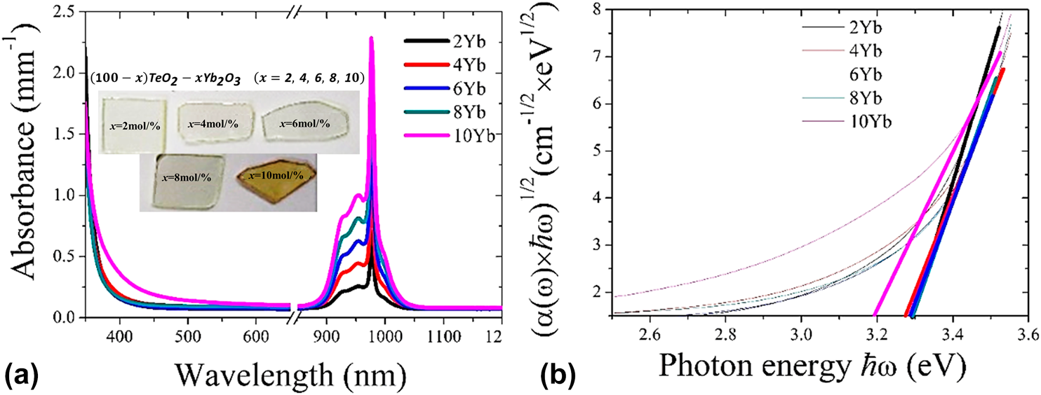
A simple composition of TeO2–Yb2O3 binary glass was selected as the host glass matrix for discussing the structure of tellurite glass with increasing Yb2O3 content. Raman spectra were measured to investigate the structure of the binary tellurite glasses, and upconversion and downconversion fluorescence characteristics were employed for discussing the relationship between the structural units and the state of Yb3+ in the tellurite glasses. The results suggested that the decrease of TeO4/2 in the glasses would result in the formation of Yb3+ clusters and Yb3+–O2− couple in the tellurite glasses, and then results in the decrease of cooperative upconversion and downconversion fluorescence intensity.
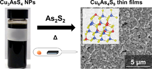
Sinnerite (Cu6As4S9) is a semiconductor computed to have attractive optoelectronic properties, but little attention has been paid to its experimental synthesis and characterization. Here, the authors report the first synthesis of polycrystalline sinnerite thin films. By heating Cu3AsS4 nanoparticles in sealed ampoules with As2S2 powder, a phase transformation to Cu6As4S9 is achieved along with the formation of micron-sized dense grains appropriate for device applications. The films display a bandgap of ~1.2 eV, significant photocurrent generation under simulated AM1.5 illumination, and carrier lifetimes nearing 1 ns, demonstrating the promise of sinnerite for use in photovoltaic applications.
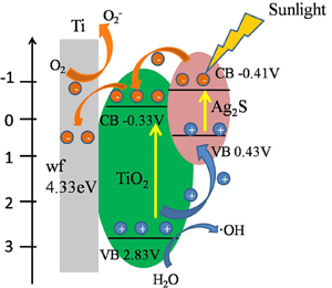
The narrow bandgap of Ag2S quantum dots was used to decorate TiO2 nanotube arrays (TiO2 NTAs) by the successive ionic layer adsorption and reaction (SILAR) method to enhance its photoelectrochemical performance. The micromorphology of the photoanode films prepared by the SILAR under different parameters (including different cycle times, capillary spot sample, and ultrasound-assisted) was systematically analyzed. The photoanode film Ag2S/TiO2 prepared by the SILAR under the ultrasound-assisted method shows Ag2S evenly distributed in TiO2 NTAs. At the same time, the corresponding photoabsorption range has been extended to the visible area, while the photocurrent density and photoconversion efficiency have been increased to ~1.8 mA/cm2 and 0.6%, respectively.